Modeling and Analysis of Composite Antenna Superstrates Consisting on Grids of Loaded Wires
Abstract
We study the characteristics and radiation mechanism of antenna superstrates based on closely located periodical grids of loaded wires. An explicit analytical method based on the local field approach is used to study the reflection and transmission properties of such superstrates. It is shown that as a result of proper impedance loading there exists a rather wide frequency band over which currents induced to the grids cancel each other, leading to a wide transmission maximum. In this regime radiation is produced by the magnetic dipole moments created by circulating out-of-phase currents flowing in the grids. An impedance matrix representation is derived for the superstrates, and the analytical results are validated using full-wave simulations. As a practical application example we study numerically the radiation characteristics of dipole antennas illuminating finite-size superstrates.
Index Terms:
Superstrate, wire grid, capacitively loaded wire, local field, gain enhancementI Introduction
Artificial dielectrics, implemented e.g. as arrays of wires, have been used for decades as light-weight beam shaping elements, see e.g. [1]–[6] for some early contributions and [7, 8] for some more recent results. It is nowadays well understood that some electromagnetic (photonic) crystals simulate the behavior of homogeneous materials with ultra-low refractive index near stop-band edges [9, 10, 11]. This observation has lead to several studies concerning directive antenna design using such periodical structures to shape the beam of a low-gain primary radiator, e.g. [12]–[14]. It is also known that a slight local change in the period of electromagnetic crystals leads to localized resonant modes which can be used for the realization of devices radiating energy in a very narrow angular range [15]. Typically, radiating sources are placed inside Fabry-Perot resonant cavities formed by removal of rows of wires or dielectric rods in a periodical lattice [16]–[21]. The long-known ideas of creating resonant cavities using partially reflecting sheets [22] have also been widely employed in recent gain enhancement designs [23]–[27]. Similarly, frequency-selective surfaces on top of ground planes have been used to implement Fabry-Perot resonant cavities, e.g. [28]. Antenna superstrates are another well-known gain enhancement tool [29, 30]. As in the case of defected electromagnetic crystal structures [16]–[21] one of the key ideas of different superstrates is to allow radiation from a primary source to spread over a larger radiating aperture. Recently, very exotic structures such as material covers or superstrates aimed to possess double-negative behavior [31] have been proposed for this purpose [32, 33, 34].
The goal of this work is to present an analytical methodology for studying the characteristics of a class of composite structures proposed as superstrates for low-gain antennas. More precisely, we consider two closely located parallel grids of capacitively loaded wires having possibly a grid of continuous (purely inductive) wires in between them. The methodology presented here can, however, be extended to study the characteristics of other kinds of superstrates based on multiple grids of wires loaded with arbitrary distributed impedance. The physical mechanism responsible for the operation of the proposed superstrates is clarified. We also briefly discuss the extension of the methodology to handle strongly coupled dipole grids. The transmission properties of such grids have in the past been analyzed with an application to frequency-selective surfaces or electromagnetic band-gap structures, e.g., in [36, 37, 38]. In these works the response has been calculated using an iterative method based on solving a set of coupled integral equations for the unknown element currents and aperture fields. The method presented here is explicit, and despite taking into account all the near field interactions between the grids (higher-order Floquet modes) it remains computationally efficient and physically illustrative.
The novelty of the proposed superstrate designs is to excite resonant oscillations in capacitively loaded wires (this way creating a wider radiating aperture) while maintaining partial transparency of the structure. In the designs considered here the source field induces out-of-phase currents to the loaded wire pairs, and the pairing currents give rise to resonant magnetic dipole moments that produce aperture radiation. After heuristically explaining the operational principle of the proposed superstrates we move on calculating the reflection and transmission properties of the superstrates. The analytical results are validated using full-wave simulations, and for a physical illustration we calculate the electric and magnetic dipole moments induced to one of the structures. It is shown that strong resonant enhancement of the superstrate aperture field can be achieved with very thin structures. To further clarify the physics behind the superstrate operation we derive an impedance matrix representation directly from the electrodynamic model. Finally, a high-gain antenna structure utilizing the proposed superstrates is implemented in a commercial method-of-moments solver.
II Heuristic operational principle
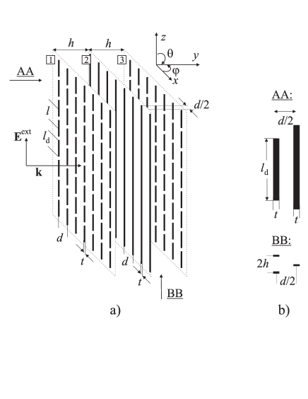
The superstrate studied in this work is schematically depicted in Fig. 1a. The first and third grids (see the numbering of grids in Fig. 1a) consist of parallel capacitively loaded111In this work capacitive loading is created by cutting the wires. wires, while the second grid consists of continuous (inductive) thin wires. Please note that in Fig. 1 round wires have been replaced by strips to reflect one feasible implementation technique. However, in the following analytical derivation we assume round wires since electrically thin wires and strips behave in a similar manner. To account for the difference in the geometry an effective radius of wires is introduced in the analytical analysis.
The properly designed structure is expected to show an analogy with double-negative behavior: In a certain frequency range the metal strips constituting a capacitively loaded wire can be interpreted as short dipoles, and every pair of such dipoles (sitting in grids 1 and 3) shows a magnetic resonant mode which can be utilized to create a response similar to that of split rings [39, 40]. On the other hand, the long conductors provide plasma-like electric response as in wire media [41, 42]. Recently, it has been reported that only short wire pairs are enough to obtain double-negative behavior [43, 44]. For describing the radiation properties of the superstrate we concentrate, however, on the distributed dipole moments induced in the structure.
Consider first only a pair of two capacitively loaded wires (assuming that grid 2 is absent). At a certain frequency the currents induced to individual pairing metal strips cancel each other allowing the incident wave to propagate through the grids. To widen the pass-band one can bring a grid of solid wires in between the loaded wire grids. In this case two modes appear due to the capacitances and mutual coupling between the loaded wires and the continuous wires. In other words, there are now two possibilities for the currents in the grids to cancel each other, and by properly choosing the unit cell dimensions both transmission bands can be merged together. Since the superstrate is volumetric (though the total thickness is in practise extremely small compared with the wavelength) the cancelation of total electric current does not mean the cancelation of radiation: The amplitude of the reflection coefficient is minimized at this frequency (and consequently the amplitude of the transmission coefficient is maximized), however, the magnetic dipole moments created by the pairing out-of-phase currents produce radiation.
Another important practical issue, discussed below in more detail, is the interaction between a closely located primary radiator and the loaded wire grids. It will be shown that in case of capacitively loaded wires the source can be brought very close to the grids without deteriorating the radiation resistance. This allows us to design low-profile and effectively radiating structures.
III Local field method to study the superstrate properties
III-A Plane-wave reflection and transmission coefficients and induced electric and magnetic dipole moments
At this point we assume that the grids in the superstrate are infinite in the and directions. Moreover, the transversal thickness of the inclusions (equivalently the radius of round wires) is small compared to the wavelength. We assume the normal plane-wave incidence (though the analysis can be carried out for oblique incidence as well) and write the external electric field as
| (1) |
We write down the equation for the local electric field acting on the surface of a reference element in each of the grids. Consider first the unloaded reference wire, and assume that the wires are thin enough so that we can represent them as infinitely long current lines located at the wire’s axes. The relation between the amplitude of the local electric field acting on the wire surface and current flowing on the wire surface reads
| (2) |
where is the susceptibility of the wire which can be determined from the boundary condition on the wire surface (see e.g. [45]):
| (3) |
where is the wave impedance in the matrix material (host material for the wires), and represents the Hankel function of the second kind and zero order. If the wires are loaded with a certain uniformly distributed impedance per unit length , the inverse of the wire susceptibility becomes [35, 46]:
| (4) |
The amplitude of the local electric field acting on the reference wires can also be expressed in the following manner:
| (5) |
| (6) |
| (7) |
where () is the amplitude of current induced to the grid , and is so called self interaction coefficient (eq. (11) in [41], see also [47]):
| (8) |
and are mutual interaction coefficients (eqs. (12) and (13) in [41]):
| (9) |
Above is the Euler constant, and is the -component of the -th Floquet mode wave vector [41]:
| (10) |
Physically tells how strongly the wires located in the same grid as the reference wire influence the local field, whereas measure the influence of the other two grids. Now we can cast eqs. (5)–(7) in the following form:
| (11) |
From the above equation currents in different grids can be solved by simple inversion. The averaged current density induced to the grids is defined as
| (12) |
In the far zone, the reflected field of one grid is a plane-wave field, and in the grid plane this plane-wave field can be expressed as [46]
| (13) |
After this we can calculate the total reflection and transmission coefficients. The reflection and transmission coefficients referred to the plane of the first grid read:
| (14) |
| (15) |
As an example, we calculate the dipole moments induced to the structure consisting of two grids of capacitively loaded wires (in this case grid 2 is absent in Fig. 1a). The electric and magnetic dipole moments confined in the unit volume (Fig. 1b) are calculated as [48]
| (16) |
| (17) |
where is the charge density in the unit volume, and J is the corresponding volumetric current density. When the integrations are conducted in our geometry the dipole moments take the following form:
| (18) |
| (19) |
III-A1 Discussion on the modeling approach
It is known that at low frequencies (frequencies at which the structural dimensions are small compared to the wavelength) the dispersion properties of lattices of capacitively loaded wires and dipole scatterers rather closely resemble each other [35]. Noticeable deviation is seen only close to the frequencies where the strip length in the loaded wires becomes resonant. At these frequencies (and at higher frequencies), for accurate analysis one should model the first and third grids as grids of dipole scatterers. The principal ideas of the above derivation would still be the same, however, different models for inclusion polarizabilities and interaction constants should be used [49]–[51].Thus, a similar local field approach as introduced in the present paper can also be used to treat grids in which the unit inclusions can be modeled as small dipole scatterers. It will be demonstrated below that in the frequency regime where the superstrates proposed in this paper are feasible for antenna beam shapers, the capacitively loaded wire model leads to accurate results. It is also important to note that the method described above can be used to study the properties of superstrates formed by an arbitrary number of grids, and the distributed impedance loading the wires can be arbitrary.
III-A2 Numerical validation
For the validation of the analytical method we choose for the superstrate the structural parameters considered in [34] (the notation is clear from Fig. 1): mm, mm, mm, mm, mm. We introduce equivalent round-cross-section wires, and use text book formulas to estimate the distributed capacitance due to the slits in the wires in first and third grids.
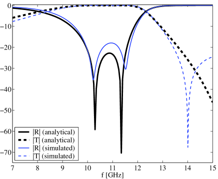
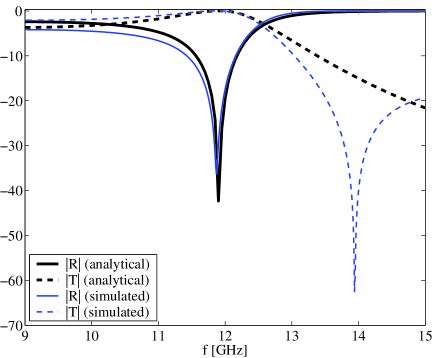
For calculating the reflection and transmission coefficients we consider separately two structures. In the first one only the two grids of capacitively loaded wires are present. In the second case we bring the grid of continuous wires in between the loaded wire grids as shown in Fig. 1a. Reflection and transmission coefficients are calculated using eqs. (14) and (15). We also simulate the coefficients using Ansoft HFSS [52] (the unit cell for HFSS simulations is shown in Fig. 1b). The results of calculations and simulations are depicted in Figs. 2 and 3. We observe that the agreement between the analytical calculations and simulations is good up to 13 GHz. At this frequency the length of the metal strips in the loaded wires is already roughly , so it is clear that at frequencies higher than 13 GHz (in this particular case) the local field model based on loaded wires fails. Nevertheless, for antenna applications we are interested in the frequency regime where the superstrates are partially transparent (frequency regime in which the reflection minima and transmission maxima lie, see Figs. 2 and 3), and at these frequencies the analytical model works well.
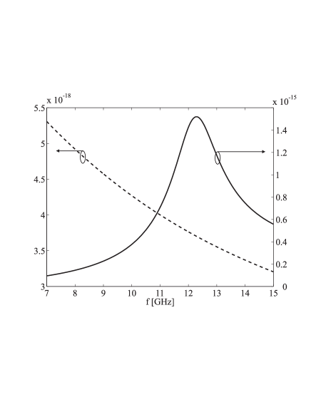
The amplitudes of electric and magnetic dipole moments induced in the unit volume of the superstrate consisting of two grids of loaded wires are shown in Fig. 4. As speculated earlier, the magnetic dipole moment shows a strong resonance in the vicinity of the frequency where the plane-wave reflection coefficient is minimized. It is worth to note that at the frequency of magnetic resonance the thickness of the superstrate is only .
III-B Impedance matrix representation
Based on the analysis of induced currents we derive an impedance matrix representation [53] connecting the total (averaged) electric field in the grid planes to the averaged current densities flowing in the grids:
| (20) |
Such representation is useful, e.g., when representing the grids as equivalent discrete loads in a waveguide modeling free space plane-wave propagation [3]. The expressions deduced below allow also to represent the mutual interaction between the grids at the impedance description level. In the quasi-static limit the deduced impedance expressions can be used to construct an equivalent circuit for the superstrates. For the sake of clarity we conduct below the derivation for the first grid in details.
Using the impedance matrix notation the total field in the plane of the first grid reads
| (21) |
Following the definition of the impedance matrix [53], is the total electric field in the first grid plane divided by the averaged current flowing in that grid, assuming that currents in the other grids are zero. The component of the total (averaged) electric field parallel to the grids, defined in the plane of grid is by definition [46]
| (22) |
When we solve from (5) (now ) and substitute the result in (22), the following expression is obtained:
| (23) |
Next, consider the definition of . The plane-wave term disappears in (22) since now the current flowing in the first grid is by definition zero [53]. Thus, we get (after we solve from (5) assuming that ):
| (24) |
Similarly for :
| (25) |
After repeating the above procedure for the second and third grid we get the following expressions for the impedances:
| (26) |
| (27) |
| (28) |
| (29) |
IV Finite size superstrates illuminated by wire antennas
In this section we study and discuss the performance of finite-size superstrates when illuminated by practical antennas. Throughout the rest of the paper our primary source is a resonant -dipole antenna. Naturally, the superstrates could also be illuminated with other types of antennas, such as with microstrip antennas, for example.
IV-A Large superstrate with infinitely long wires
Before designing an actual prototype antenna we study how well the key ideas for the superstrate performance, outlined with the plane-wave excitation, apply when the superstrates are illuminated with a resonant dipole, and the number of wires in the superstrates is finite. Namely, we study possible cancelation of electric currents in such structures. To avoid the standing wave interference caused by a finite wire height, and more clearly see the possible cancelation effect, we assume in this subsection that the wires are infinitely long. To ease the physical interpretation we consider here only the structure containing two grids of loaded wires, since in this case there is only one possibility (one frequency) for the cancelation of the total electric current, please see Fig. 3. Later, when designing the prototype antenna we consider also the superstrate containing a grid of unloaded wires.
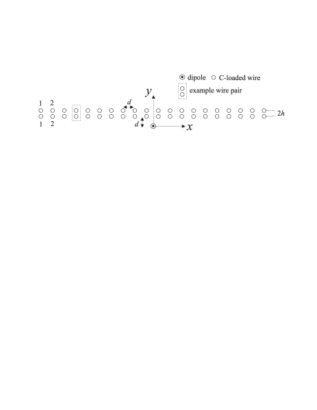
The number of wires in the grids is fixed to be 20, and we also fix the source position, see Fig. 5. The structural parameters are the same as introduced in Section III A. To handle the infinite wire length we use the method described in [54] to solve the currents induced to the grids by taking into account the dipole excitation and the mutual interaction between all the wires. The distribution of induced current (amplitude and phase) is studied at three different frequencies, namely at , , and GHz. Based on the result in Fig. 3 we predict that 11.9 GHz corresponds to the frequency at which the amplitude of current induced to the pairing wires is more or less the same, but the phase difference between the pairing currents is roughly .
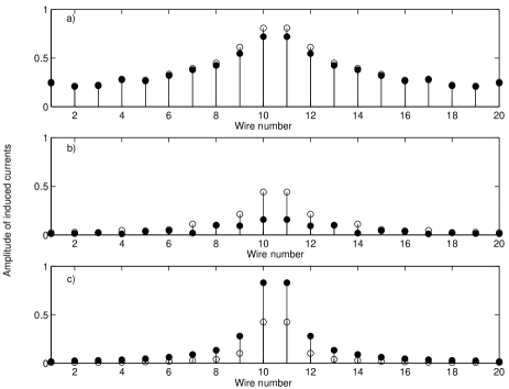
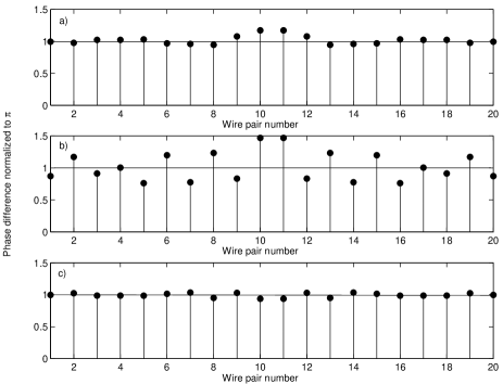
The amplitudes of the currents induced to the pairing wires are shown in Fig. 6 (the feed current amplitude equals unity). The phase differences of currents induced to the pairing wires are depicted in Fig. 7. We observe that at 11.9 GHz the amplitudes of currents induced to the pairing wires are close to the same value in most of the pairs. Slight difference is seen only in the wires closest to the dipole, but this difference is compensated by the fact that also the phase difference between the currents induced to the corresponding wire pairs slightly differs from . In those wire pairs where the current amplitudes are practically the same, also the phase difference is practically . The aforementioned implies that, indeed, the total electric current induced to the grids cancels as was speculated already in Section II. At 10.4 GHz the amplitudes of induced currents are much lower than at 11.9 GHz. Also the amplitudes of several pairing currents considerably differ from each other, and in many pairs the phase difference between the currents considerably differs from . Even though the phase differences of pairing currents is close to in all the pairing wires at 13.4 GHz (Fig. 7c), the total electric current is not canceled at this frequency since the amplitudes of currents constituting the pairs differ from each other in many pairs, Fig. 6c.
IV-B High-gain antenna structure utilizing the proposed superstrates
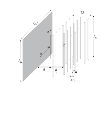
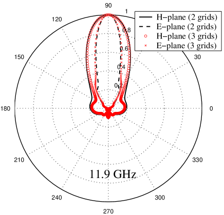
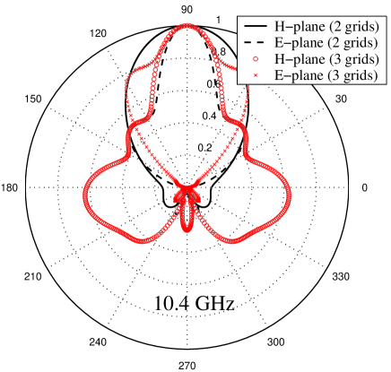
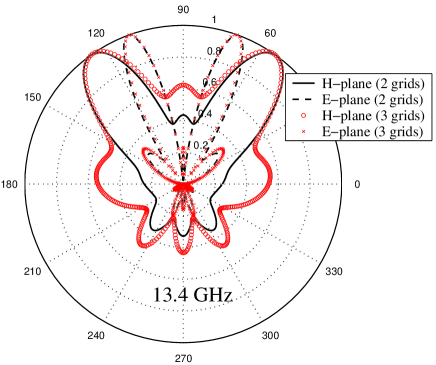
In this subsection we design and implement a high-gain prototype antenna in a commercial method-of-moments solver FEKO [55]. The schematic illustration of the studied antenna structure is depicted in Fig. 5. We consider separately two structures: In the first case the grid of unloaded wires is absent (when analyzing the results we call this case the “2 grids” case), and in the second case the structure is as depicted in Fig. 8 (“3 grids”). The radiation characteristics of both antenna structures are studied at the three frequencies introduced in the previous subsection.
The dipole length is tuned to be at every considered frequency. The wire length is fixed to be at 11.9 GHz. Also the width (in -direction) of the superstrate is approximately at 11.9 GHz. To enhance the directivity of the antenna structure, and make it more attractive as a possible high-gain solution, we create a resonant cavity using a metal reflector behind the grids, Fig. 8. Some of the available earlier contributions concerning the implementation of Fabry-Perot resonant cavities using partially reflecting sheets or other structures are listed in the Introduction. The distance between the metal reflector and the first wire grid equals which roughly corresponds to at 11.9 GHz. The other relevant structural parameters are the same as introduced in connection with the plane-wave analysis (see Section III A).222In FEKO we model round wires, and the capacitance caused by slits in the strips is modeled as an equivalent bulk capacitor. In the following the horizontal plane (H-plane) corresponds to the plane perpendicular to the wires, and vertical (E-plane) corresponds to the plane parallel to the wires.
IV-B1 Example results
For this study the interesting antenna characteristics are the antenna radiation pattern, the input impedance , and the maximum boresight directivity . We have not performed any systematic optimization of one or more of these characteristics, thus, from many points of view the presented antenna performance might not be optimal. The reader is also reminded that compared to the situation analyzed in Section III where the number of wires is infinite in the -direction and the wire length is infinite, the finite number of wires and the finite wire height lead to the formation of standing waves along and -directions. This standing wave formation depends also on the location of the source, and it rather strongly influences the radiation characteristics.
The simulated radiation patterns are depicted in Figs. 9–11, and the main simulated radiation characteristics are gathered in Table I. Even without systematically optimizing the structural parameters we observe a good boresight directivity at 11.9 GHz, which is consistent with the analysis presented so far in this paper. For comparison, without the superstrate the boresight directivity of a metal-plate backed dipole is 8.5 dB. In addition to this, the input resistance (in case of lossless structures, the radiation resistance) is high and makes the antenna easy to match to a standard 50 Ohm cable. It was analytically shown in [56] that when a wire antenna is positioned in close vicinity of capacitively loaded wires, the currents induced to the closest wires add up constructively with the source current, and therefore the radiation resistance remains high. This, indeed, appears to be the case. For comparison, in case when all the wires depicted in Fig. 8 are unloaded, the simulated input resistance at 11.9 GHz is only 0.7 Ohm.
At 10.4 and 13.4 GHz the radiation characteristics are not so favorable for a feasible high-gain solution. At 10.4 GHz the peak directivity is weaker with both superstrates partly because the resonant cavity is not tuned for this particular frequency, and partly because the effective superstrate aperture is smaller than at 11.9 GHz. We see from Fig. 2 that the plane-wave reflection coefficient of the 3-grid superstrate is still very small at 10.4 GHz due to the dual resonance behavior. The corresponding effect is possibly seen as a much more narrow beamwidth of the main lobe (in boresight direction) as compared with the 2-grid structure. However, the finite structural dimensions clearly cause diffraction in the backward and sidelobe directions, and therefore the obtained maximum directivity is only moderate. We believe, however, that after optimizing the structure at 10.4 GHz the directivity could be enhanced (if desired antenna performance would be required over a wider frequency band). At 10.4 GHz and also at 13.4 GHz the input resistance is visibly smaller than at 11.9 GHz, and this might lead to difficulties in achieving high radiation efficiencies when realistic losses are taken into account (especially with the 2-grid structure at 10.4 GHz). Additional simulations (not shown) on the current distribution induced to the wires in the 2-grid superstrate indicate that at 11.9 GHz there is only one current maxima along the wires (in the -direction, Fig. 8), and the current amplitude in all the wires (excluding the two pairs of wires closest to the dipole) is rather close to the same value. This means that the superstrate aperture is rather uniformly excited, and a good boresight directivity is expected. At 10.4 GHz only every second pair is strongly excited. This is also the case at 13.4 GHz, in addition to this, at 13.4 GHz standing waves with three current maxima in -direction are induced to the wires, and this is seen as the beam splitting in the E-plane.
| 2 grids | ||
| [GHz] | [Ohm] | [dB] |
| 11.9 | 50.2 + j86.8 | 15.3 |
| 10.4 | 15.2 + j82.2 | 9.8 |
| 13.4 | 33.3 + j96.2 | |
| 3 grids | ||
| [GHz] | [Ohm] | [dB] |
| 11.9 | 50.3 + j87.7 | 15.0 |
| 10.4 | 33.0 + j96.5 | 9.0 |
| 13.4 | 36.7 + j95.8 | † |
† The maximum of directivity does not occur in the boresight direction.
V Conclusion
We have presented a method to analyze the characteristics of a class of antenna superstrates based on periodical grids of loaded and unloaded wires. In addition to this, the physics behind the radiation mechanism of such superstrates has been clarified. The local field method has been used to solve the currents induced to the superstrates by the incident plane-wave field, and the reflection and transmission properties of the superstrates have been studied. The analytical results have been verified using numerical simulations. As a practical application example we have considered finite-size superstrates illuminated by dipole antennas, and discussed the effects of finite structural dimensions to the superstrate performance. A high-gain antenna structure utilizing the proposed superstrates has been implemented in a commercial full-wave simulator, and the results show promising antenna performance.
Acknowledgement
One of the authors (P.M.T. I.) wishes to thank Dr. Pavel A. Belov for useful discussions related to the wire media modeling.
References
- [1] W. E. Kock, “Metal-lens antennas,” Proc. IRE, vol. 34, pp. 828–836, 1946.
- [2] ——, “Metallic delay lenses,” Bell System Technical J., vol. 27, pp. 58–82, 1948.
- [3] J. B. Brown, “Artificial dielectrics,” in Progress in Dielectrics, 2nd ed., J. B. Birks and J. H. Schulman, Eds. London: Heywood Co. Ltd., 1960, pp. 193- 225.
- [4] W. Rotman, “Plasma simulation by artificial dielectrics and parallel plate media,” IRE Trans. Antennas Propag., vol. 10, pp. 82–95, 1962.
- [5] K. E. Golden, “Plasma simulation with an artificial dielectric in a horn geometry,” IEEE Trans. Antennas Propag., vol. 13, no. 4, pp. 587–594, 1965.
- [6] I. J. Bahl and K. C. Gupta, “A leaky-wave antenna using an artificial dielectric medium,” IEEE Trans. Antennas Propag., vol. 22, no. 1, pp. 119–122, 1974.
- [7] P. Ikonen, C. Simovski, and S. Tretyakov, “Compact directive antennas with a wire-medium artificial lens,” Microwave Opt. Technol. Lett., vol. 43, no. 6, pp. 467–469, 2004.
- [8] P. Ikonen, M. Kärkkäinen, C. Simovski, P. Belov, and S. Tretyakov, “Light-weight base station antenna with artificial wire-medium lens,” IEE Proc. Microwaves, Antennas and Propag., vol. 153, no. 2, pp. 163–170, 2006.
- [9] B. Gralak, S. Enoch, and G. Tayeb, “Anomalous refractive properties of photonic crystals,” J. Opt. Soc. Am. B, vol. 17, no. 6, pp. 1012–1020, 2000.
- [10] M. Notomi, “Theory of light propagation in strongly modulated photonic crystals: Refractionlike behavior in the vicinity of the photonic band gap,” Phys. Rev. B, vol. 62, no. 16, pp. 10696 -10705, 2000.
- [11] B. T. Schwartz and R. Piestun, “Total external reflection from metamaterials with ultralow refractive index,” J. Opt. Soc. Am. B, vol. 20, no. 12, pp. 2448–2453, 2003.
- [12] S. Enoch, G. Tayeb, P. Sabouroux, N. Guérin, and P. Vincent, “A metamaterial for directive emission,” Phys. Rev. Lett., vol. 89, no. 21, 2139021, 2002.
- [13] S. Enoch, G. Tayeb, and B. Gralak, “The richness of the dispersion relation of electromagnetic band-gap materials,” IEEE Trans. Antennas Propag., vol. 51, no. 10, pp. 2659–2666, 2003.
- [14] G. Lovat, P. Burghignoli, F. Capolino, D. R. Jackson, and D. R. Wilton, “Analysis of directive radiation from a line source in a metamaterial slab with low permittivity,” IEEE Trans. Antennas Propag., vol. 54, no. 3, pp. 1017–1030, 2006.
- [15] G. Tayeb and D. Maystre, “Rigorous theoretical study of finite-size two-dimensional photonic crystals doped by microcavities,” J. Optical Soc. America A, vol. 14, no. 12, pp. 3323–3332, 1997.
- [16] M. Thévenot, C. Cheype, A. Reineix, and B. Jecko, “Directive photonic-bandgap antennas,” IEEE Trans.M̃icrowave Theory Tech., vol. 47, no. 11, pp. 2115–2122, 1999.
- [17] B. Temelkuran, M. Bayindir, E. Ozbay, R. Biswas, M. M. Sigalas, G. Tuttle, and K.-M. Ho, “Photonic crystal-based resonant antenna with a very high directivity,” J. Appl. Phys., vol. 87, no. 1, pp. 603–605, 2000.
- [18] R. Biswas, E. Ozbay, B. Temelkuran, M. Bayindir, M. M. Sigalas, and K.-M. Ho, “Exceptionally directional sources with photonic-bandgap crystals,” J. Opt. Soc. Am. B, vol. 18, no. 11, pp. 1684–1688, 2001.
- [19] C. Cheype, C. Serier, M. Thévenot, T. Monédiére, A. Reineix, and B. Jecko, “An electromagnetic bandgap resonator antenna,” IEEE Trans. Antennas Propag., vol. 50, no. 9, pp. 1285–1290, 2002.
- [20] T. Akalin, J. Danglot, O. Vanbésien, and D. Lippens, “A highly directive dipole antenna embedded in a Fabry-Perot type cavity,” IEEE Microw. Wireless Comp. Lett., vol. 12, no. 2, pp. 48–50, 2002.
- [21] Y. J. Lee, J. Yeo, R. Mittra, and W. S. Park, “Application of electromagnetic bandgap (EBG) superstrates with controllable defects for a class of patch antennas as spatial angular filters,” IEEE Trans. Antennas Propag., vol. 53, no. 1, pp. 224–235, 2005.
- [22] G. von Trentini, “Partially reflecting sheet arrays,” IRE Trans. Antennas Propag., vol. 4, pp. 666-671, 1956.
- [23] A. P. Feresidis and J. C. Vardaxoglou, “High gain planar antenna using optimized partially reflective surfaces,” IEE Proc. Microwaves, Antennas and Propag., vol. 148, no. 6, pp. 345–350, 2001.
- [24] G. K. Palikaras, A. P. Feresidis, and J. C. Vardaxoglou, “Cylindrical electromagnetic bandgap structures for directive base station antennas,” IEEE Antennas Wireless Propag. Lett., vol. 3, pp. 87–89, 2004.
- [25] A. P. Feresidis, G. Goussetis, S. Wang, and J. C. Vardaxoglou, “Artificial magnetic conductor surfaces and their application to low-profile high-gain planar antennas,” IEEE Trans. Antennas Propag., vol. 53, no. 1, pp. 209–215, 2005.
- [26] S. Wang, A. P. Feresidis, G. Goussetis, and J. C. Vardaxoglou, “High-gain subwavelength resonant cavity antennas based on metamaterial ground planes,” IEE Proc. Microwaves, Antennas and Propag., vol. 153, no. 1, pp. 1–6, 2006.
- [27] H. Boutayeb and T. A. Denidni, “Analysis and design of a high-gain antenna based on metallic crystals,” J. Electromagn. Waves and Appl., vol. 20, no. 5, pp. 599–614, 2006.
- [28] Y. J. Lee, J. Yeo, R. Mittra, and W. S. Park, “Design of a high-directivity electromagnetic band gap (EBG) resonator antenna using a frequency-selective surface (FSS) superstrate,” Microwave Opt. Technol. Lett., vol. 43, no. 6, pp. 462–467, 2004.
- [29] N. G. Alexópoulos and D. R. Jackson, “Fundamental superstrate (cover) effects on printed circuit antennas,” IEEE Trans. Antennas Propag., vol. AP–32, no. 8, pp. 807–816, 1984.
- [30] D. R. Jackson and N. G. Alexópoulos, “Gain enhancement methods for printed circuit antennas,” IEEE Trans. Antennas Propag., vol. AP–33, no. 9, pp. 976–987, 1985.
- [31] D. R. Smith, W. J. Padilla, D. C. Vier, S. C. Nemat-Nasser, and S. Schultz, “Composite medium with simultaneously negative permeability and permittivity,” Phys. Rev. Lett., vol. 84, no. 18, pp. 4184–4187, 2000.
- [32] R. W. Ziolkowski and A. D. Kipple, “Application of double negative materials to increase the power radiated by electrically small antennas,” IEEE Trans. Antennas Propagat., vol. 51, no. 10, pp. 2626–2640, 2003.
- [33] B.-I. Wu, W. Wang, J. Pacheco, X. Chen, J. Lu, T. M. Grzegorczyk, J. A. Kong, P. Kao, P. A. Theophelakes, M. J. Hogan, “Anisotropic metamaterials as antenna substrate to enhance directivity,” Microwave. Opt. Technol. Lett., vol. 48, no. 4, pp. 680–683, 2006.
- [34] E. Saenz, R. Gonzalo, I. Ederra, and P. de Maagt, “Design of a planar meta-surface based on dipoles and wires for antenna applications,” in Proc. EuCAP 2006, Nice, France, Nov. 6–10, 2006, paper 349401.
- [35] P. A. Belov, C. R. Simovski, S. A. Tretyakov, “Two-dimensional electromagnetic crystals formed by reactively loaded wires,” Phys. Rev. E., vol. 66, 036610, 2002.
- [36] D. Lockyer, C. Moore, R. Seager, R. Simpkin, and J. C. Vardaxoglou, “Coupled dipole arrays as regonfigurable frequency selective surfaces,” Electron. Lett., vol. 30, no. 16, pp. 1258–1259, 1994.
- [37] J. C. Vardaxoglou and D. Lockyer, “Modified FSS response from two sided and closely coupled arrays,” Electron. Lett., vol. 30, no. 22, pp. 1818–1819, 1994.
- [38] A. P. Feresidis, G. Apostolopoulos, N. Serfas, and J. C. Vardaxoglou, “Closely coupled metallodielectric electromagnetic band-gap structures formed by double-layer dipole and tripole arrays,” IEEE Trans. Antennas and Propag., vol. 52, no. 5, pp. 1149–1158, 2004.
- [39] J. B. Pendry, A. J. Holden, D. J. Robbins, and W. J. Stewart, “Magnetism from conductors and enhanced nonlinear phenomena,” IEEE Trans. Microw. Theory Tech., vol. 47, no. 11, pp. 2075- 2084, 1999.
- [40] G. Dolling, C. Enkrich, M. Wegener, J. F. Zhou, C. M. Soukoulis, and S. Linden, “Cut-wire pairs and plate pairs as magnetic atoms for optical metamaterials,” Opt. Lett., vol. 30, no. 23, pp. 3198–3200, 2005.
- [41] P. A. Belov, S. A. Tretyakov, A. J. Viitanen, “Dispersion and reflection properties of artificial media formed by regular lattices of ideally conducting wires,” J. Electromagn. Waves and Appl., vol. 16, no. 8, pp. 1153–1170, 2002.
- [42] S. I. Maslovski, S. A. Tretyakov, and P. A. Belov, “Wire media with negative effective permittivity: A quasi-static model,” Microwave Opt. Technol. Lett., vol. 35, no. 1, pp. 47- 51, 2002.
- [43] V. M. Shalaev, W. Cai, U. K. Chettiar, H.-K. Yuan, A. K. Sarychev, V. P. Drachev, and A. V. Kildishev, “Negative index of refraction in optical metamaterials,” Optics Lett., vol. 30, no. 24, pp. 3356–3358, 2005.
- [44] J. Zhou, L. Zhang, G. Tuttle, T. Koschny, and C. Soukoulis, “Negative index materials using simple short wire pairs,” Phys. Rev. E, vol. 73, p. 041101, 2006.
- [45] L. B. Felsen and N. Marcuvitz, Radiation and scattering of waves, Piscataway, NJ: IEEE Press, 1994.
- [46] S. Tretyakov, Analytical modeling in applied electromagnetics, Norwood, MA: Artech House, 2003.
- [47] V. V. Yatsenko, S. A. Tretyakov, S. I. Maslovski, A. A. Sochava, “Higher order impedance boundary conditions for sparse wire grids,” IEEE Trans. Antennas Propag., vol. 48, no. 5, pp. 720–727, 2000.
- [48] J. D. Jackson, Classical electrodynamics, 3rd ed., New York: John Wiley & Sons, 1999.
- [49] S. I. Maslovski and S. A. Tretyakov, “Full-wave interaction field in two-dimensional arrays of dipole scatterers,” Int. J. Electron. Commun. (AEU), vol. 53, no. 3, pp. 135- 139, 1999.
- [50] V. V. Yatsenko, S. I. Maslovski, and S. A. Tretyakov, “Electromagnetic interaction of parallel arrays of dipole scatterers,” in Progress in Electromagnetics Research: PIER vol. 25, pp. 285- 307, 2000.
- [51] V. V. Yatsenko, S. I. Maslovski, S. A. Tretyakov, S. L. Prosvirnin, and S. Zouhdi, “Plane-wave reflection from double arrays of small magnetoelectric scatterers,” IEEE Trans. Antennas Propag., vol. 51, no. 1, pp. 2–11, 2003.
- [52] The www-page of Ansoft, http://www.ansoft.com.
- [53] D. M. Pozar, Microwave engineering, 2nd Ed., New York: John Wiley Sons, 1998.
- [54] S. He, C. R. Simovski, and M. Popov “An explicit and efficient method for obtaining the radiation characteristics of wire antennas in metallic photonic bandgap structures,” Microwave Opt. Techn. Lett., vol. 26, no. 2, pp. 67–73, 2000.
- [55] The www-page of FEKO, http://www.feko.info.
- [56] C. R. Simovski and S. He, “Antennas based on modified metallic photonic bandgap structures consisting of capacitively loaded wires,” Microwave Opt. Technol. Lett., vol. 31, no. 3, pp. 214–221, 2001.