LC-DET-2006-008
November 2006
A proposed DAQ system for a calorimeter at the International
Linear Collider
Abstract
This note describes R&D to be carried out on the data acquisition system for a calorimeter at the future International Linear Collider. A generic calorimeter and data acquisition system is described. Within this framework modified designs and potential bottlenecks within the current system are described. Solutions leading up to a technical design report will to be carried out within CALICE-UK groups.
M. Wing1,†, M. Warren1, P.D. Dauncey2 and J.M. Butterworth1
for CALICE-UK groups
1University College London, 2Imperial College London
†Contact: mw@hep.ucl.ac.uk
1 Introduction
With the decision on the accelerator technology to be used for a future International Linear Collider (ILC), detector R&D can become more focused. The time-line for an R&D programme is also clearer with, assuming a technical design report to be written by 2009, three years to define the make-up of a given sub-detector. Within the CALICE collaboration, which is designing a calorimeter for the ILC, a collection of UK groups (CALICE-UK) are part of the initial effort to prototype a calorimeter composed of silicon and tungsten [1]. The electromagnetic section of the calorimeter (ECAL) has been taking test-beam data at DESY and CERN in 2006. The UK has designed and built electronics to readout the ECAL [4] - these are also now being used by the analogue hadronic calorimeter - and is taking part in the current data-taking period. Building on this expertise, CALICE-UK has defined an R&D programme. A significant part of this programme is the design of the data acquisition (DAQ) system for a future calorimeter.
In the work, DAQ equipment will be developed which attacks likely bottlenecks in the future system and is also sufficiently generic to provide the readout for new prototype calorimeters, such as the prototype to be built in the EUDET project [5]. The main aim is to start an R&D programme which will work towards designing the actual DAQ system of the future calorimeter. Alternative designs of a DAQ system which could affect the layout of the final detector or functionality of components are also considered. The concept of moving towards a “backplaneless” readout is pursued. A strong under-pinning thread here is to attempt to make use of commercial components and identify any problems with this approach. Therefore the system should be easily upgradable, both in terms of ease of acquiring new components and competitive prices.
This note is organised as follows. The parameters of the superconducting accelerator design and calorimeter structure and properties which impinge upon considerations of the DAQ system for a calorimeter are discussed in Section 2. The main body of the note in Section 3 discusses the DAQ design and proposes areas of R&D within it. The work is will investigate the three principal stages of the DAQ system: the connection along the calorimeter module; the connection from the on- to off-detector; and the off-detector receiver. In Section 4 a model DAQ system for the final ECAL is proposed. This necessarily makes many assumptions but gives an idea of the scale of the system involved: it can also be the start of an initial costing. The note ends with a brief summary in Section 5.
The programme detailed below will allow CALICE-UK groups to continue to assist in development of new technologies for the DAQ system. We would expect to write a chapter in the future technical design report on the DAQ system for the calorimeter. For the final calorimeter, the DAQ should ideally be the same for the ECAL and HCAL. Although CALICE-UK has so far concentrated on the ECAL, our proposals for R&D contained in this document are sufficiently generic that both calorimeter sections should be able to converge to use the DAQ system we design. This will place us in a position to build the DAQ system for future large-scale prototype calorimeters (e.g. EUDET) and the final system. Indeed the principle of a generic design using commercial components should be applicable to many detector sub-systems. Therefore, the R&D to be performed here may have consequences or applications to the global DAQ system for a future detector.
2 General detector and accelerator parameters
The design [1] for a calorimeter for the ILC poses challenges to the DAQ system mainly due to the large number of channels to be read out. The TESLA design [1] for a sampling electromagnetic calorimeter is composed of 40 layers of silicon interleaved with tungsten. The calorimeter, shown in Fig. 1, has eight-fold symmetry and dimensions: a radius of about 2 m, a length of about 5 m and a thickness of about 20 cm. Mechanically, the calorimeter will consist of 6000 slabs, of length 1.5 m, each containing about 4000 silicon p-n diode pads of 11 cm2, giving a total of 24 million pads. More recent designs for the detector collaborations consider fewer layers, 29 for LDC [2] and 30 for SiD [3], and also smaller pad sizes of 55 mm2, or even 33 mm2.

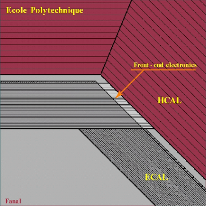
A generic scenario for the DAQ system is as follows. At the very front end (VFE), ASIC chips will be mounted on the PCBs and will process a given number of pads. The ASICs will perform pre-amplification and shaping and should also digitise the data and may even apply a threshold suppression. The current design [6] of such chips has each containing 64 channels, although this may be higher in the final calorimeter. The ASIC power consumption has to be minimised as they are difficult to cool due to the small gaps between layers which are required to take advantage of tungsten’s Molière radius. The data will be digitised in the ASIC and transferred to the front-end (FE) electronics which are placed in the detector at the end of the slab as shown in Fig. 1. It is expected that zero suppression will be done in the FE (using FPGAs) to significantly reduce the rate. The data will then be transferred off the detector, probably via a network switch, to a receiver of many PCI cards in a PC farm.
If we assume the TESLA design for data taking at 800 GeV, the following parameters have to be considered. There will be a 4886 bunch crossings every 176 ns in a bunch train, giving a bunch train length of about 860 s. The bunch train period is 250 ms, giving a duty factor between trains of about 0.35%. The ECAL is expected to digitise the signal every bunch crossing and readout completely before the next bunch train. In a shower, up to 100 particles/mm2 can be expected, which in a 11 cm2 pad equates to 10000 minimum ionising particle deposits. The ADC therefore needs a dynamic range of 14 bits. Assuming no threshold suppression and that 2 bytes are used per pad per sample, then the raw data per bunch train is 4886 2 = 250 GBytes which equates to 0.3-2.5 MBytes for each ASIC depending on whether they process between 32 and 256 channels. The data appears within a bunch train length of 860 s giving a rate out of the ASIC of 0.4-3 GBytes/s, which we take to be 1 GBytes/s from now on. Threshold suppression and/or buffering (to allow readout between bunch trains) within the ASIC could reduce this rate. However, suppression in the ASIC may not be flexible enough compared with doing this in the FE and buffering requires some ASIC power to remain on between bunch trains, potentially generating too much heat. Hence the rates after the VFE depend on the assumptions made and system layout and will be discussed for each individual case where necessary.
3 Design of a DAQ system
3.1 Transmitting digitised data from the VFE chip
The transmission of digitised data from the ASIC is very heavily influenced by what can be done within the slab given the low heat-load requirements due to the difficulties of cooling. It is not yet known what the capabilities of the VFE ASIC will be, so various possibilities were considered.
In general, somewhere in the readout system, there will have to be an ADC and a threshold discriminator. These tasks could in principle be performed in either order and could be done in the VFE or in the FE. There is also the possibility of buffering events in either the VFE or FE. This would allow the data to be read out between bunch trains rather than bunch crossings. This entails a dramatic decrease in the rate of read out due to the large spacing between bunch trains. There is then a matrix of possibilities, with some number of the functionalities, ADC, thresholding and buffering, being done in the VFE or FE. Below the four possibilities are considered for the ADC and thresholding, and also the buffering in the VFE.
-
1.
Neither ADC nor thresholding is done in the VFE
-
2.
Only the ADC is done in the VFE
-
3.
Only the thresholding is done in the VFE
-
4.
Both are done in the VFE
-
5.
Buffering done in the VFE
We consider that threshold discrimination is best done after the ADC step rather than before. This allows much easier monitoring the pedestals and noise, etc., by allowing some readout at a low rate even when below the threshold. In addition, setting a stable analogue threshold is not easy; any drifts will change the level. The uniformity over all channels might not be good enough which would then require a large number of trim DACs.
1) If neither an ADC or threshold discriminator is built into the VFE ASIC (due to them taking too much power), then the raw analogue signals will be sent out to the FE. This is 2k analogue channels which require around 14 bits precision, which is not trivial to achieve. Even if this can be done, digitising the data at the FE would be hard. The space is limited and so it is likely only a restricted number of ADCs could be mounted in this area. Assuming 20 channels of ADCs would be possible, then each would have to handle 100 pads, with these being multiplexed in turn into the ADC. To keep up with the sampling rate needed, i.e. 176 ns for each channel would therefore require the ADCs to sample at 1.76 ns. Finding a 14-bit FADC which can do this would not be easy. The alternative would be to use an analogue pipeline; assuming one for each of the 20 ADC channels would result in each pipeline storing about 500k analogue samples which is difficult. Putting an analogue threshold in front of the ADCs would clearly cut the rate down but would need a major ASIC development to handle this; a variable length analogue pipeline with time-stamps would be needed. This is in addition to the pedestal monitoring problems mentioned above.
2) Only doing the ADC on the VFE seems a much more reasonable option. The 14-bit requirement is much easier to achieve with a short signal path before the ADC. The digitised data can be transmitted from the VFE to the FE more easily than analogue data. The rates are not trivial however; these would be around 50 GByte/s per slab, or 1 GByte/s from each wafer/ASIC. This is at the level where a fibre would be needed; commercial fibres now carry 5 GBytes/s. Fibres are also less noisy than copper. This use of fibres within the slab would raise many other issues such as the power needed to transmit the light out (or could it be supplied by an external laser and then only modulated on the ASIC), how to reliably attach the fibres at each end (a total of 300 000 fibres would be needed for 6000 slabs each with 50 ASICs), how large the fibre connectors would be (the total thickness within the slabs is limited to some mm only), etc.. Although this is an active area of commercial development, it is not clear if opto-electronic intra-PCB communications will become standard enough on the time-scale needed [7].
It is clear some development would be needed for this to be an option; the equivalent system in ATLAS has three fibres transmitting a total of 10 MBytes/s with a 2 mm high connector needed. Self-aligning silicon-fibre interfaces are possibilities; while we could not do significant R&D compared with the commercial sector, we could test industrial prototypes and do R&D in conjunction with industry.
Once the data are on a fibre direct from the ASIC, the idea of whether any FE electronics would be needed at all was raised, as the fibre would go 10s of metres, bypassing the FE completely. However, shipping out all the raw data to the offline seems an expensive overkill, but is considered as this may change with commercial development.
3) Only doing the threshold in the VFE suffers from the same problems as mentioned above; there is a difficulty of monitoring the pedestals as well as the complexity of the ASIC needed to handle the channels.
4) Doing both ADC and threshold in the VFE places the easiest requirements on the FE, with a corresponding increase in difficulty for the VFE. Assuming the threshold is applied after the ADC, some communication of the threshold and other configuration data from the FE to the VFE will still be needed. The data rate out is clearly reduced; it would be around 400 MBytes/s for the slab, or 20 MBytes/s for each wafer/ASIC. Although easiest for transferring data from the VFE to FE, due to the low rates, it is not clear if the threshold can be reliably applied in the VFE. This scenario also looks like the situation if the Monolithic Active Pixel Sensors (MAPS) technology - essentially a digital calorimeter - were used rather than silicon diodes. For the diode option in this scenario, it is also questionable as to whether significant FE electronics logic is needed. As the ASIC performs both ADC and threshold suppression, the data could be transferred directly off the detector.
5) It is generally assumed that buffering in the FE is possible, with large amounts of memory available in modern FPGAs. However, the issue of buffering in the ASICs is more technically challenging. The challenges for such a procedure are having a large enough memory integrated into the ASICs and the keeping the power low whilst the data is being read out between bunch trains. The advantages are clear: the rate of transmission from the ASIC to the FPGA is reduced by about two orders of magnitude. For the proposed electrical connections along the board this will ease the transmission significantly.
We, therefore, propose R&D for two scenarios where only the ADC is done in the VFE and where the ADC and thresholding are done in the VFE, both coupled with buffering in the VFE because they provide realistic solutions and have complementary applications. In favour of only performing the ADC, any threshold suppression can be performed more accurately in the FPGA at the FE rather than in the VFE. When thresholding is also done in the VFE along with the ADC, the data transfer rate from the VFE and FE is significantly smaller. A schematic of scenario 2) is shown in Fig. 2.
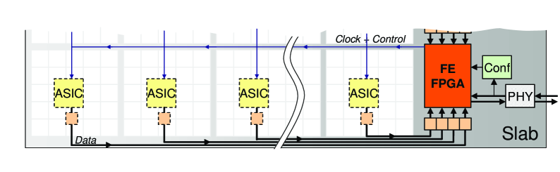
In both scenarios, we intend to set-up a mock data transfer system which requires having a test board with FPGAs linked by fibres. This will simulate a link between the VFE ASICs and the FE FPGAs. Any developed system e.g. a new VFE chip design or the MAPS set-up could also be tested in our prototype system. We will also demonstrate that the system would work for the hadronic calorimeter as well as the ECAL. This would require modifying the system to have a more links but a lower rate. The prototype will incorporate, wherever possible, commercially available components such as Virtex-4 FPGAs [8] which has multi-gigabit serial transceivers and is compatible with 10/100/1000 Mbit/s ethernet and PCI express x16 and higher.
The final chip should have around 64 channels and would be embedded inside the detector. The ADC(s) should be included in the chip in order to output digital data serially at high rate (typically 1-2Gbit/s). The DAQ would thus look more like “an event builder” than a traditional DAQ. It would perform the data reformatting (from “floating” gain + 10bit to 16 bit), calibration, possibly linearisation and some digital filtering. It is possible that at this level, some event processing will be performed. The other task of the DAQ is to load all the parameters needed by the front-end, control the power cycling and run the calibration. These specifications fit in well with our current generic system.
The current version of the VFE ASIC chip [11] is being used to read out the existing CALICE ECAL. This chip does not meet the requirements for the ILC ECAL and the development of the design is an ongoing project in LAL/Orsay [6]. In the next 1–2 years, it is expected to have a version of such a chip with low enough power and noise that would serve as a realistic prototype. This ASIC is expected to have (at least) 32 channels, an internal ADC per channel, multiple gain ranges, and optional threshold suppression and digital buffering to reduce the required output rate.
Instead of using silicon diodes, the feasibility of using the MAPS technology is to be investigated [10]. The use of this technology would also have an impact on the design of the DAQ system. Here, there would be no ADC and a threshold has to be applied on the wafer, by definition. The data rate for a final detector would be 3 GBytes/s per slab, or 150 MBytes/s per wafer, which is low enough for non-fibre communication.
If threshold suppression or buffering could be done in the VFE ASIC, the rate to the FE would be reduced by two orders of magnitude. Current designs cannot do this and it may not even be desirable or practical, so we have to allow for data rates of order GByte/s needing to be transferred out of each VFE ASIC during the bunch train. Whether an electrical or optical connection would be needed has to be investigated. Although chip-to-chip fibres are not yet standard technology, this is an active area of industrial research [7].
Issues of how the data would be transported from the VFE to FE have to be considered and can be done already without a real prototype. Transporting of order GByte/s of data over 1.5 m in a very limited space is a challenge. The conventional approach would be to use copper but here the effects of noise and interference will have to be considered. There is also the possibility of using optical fibres although here there are also design considerations: the size of connectors would have to be investigated as the vertical clearance at the VFE is of the order of mm and the power needed to transmit light out would also need to be investigated. This work ties in closely with the mechanical and thermal aspects of the design.
In preparation for a real prototype, a test system will be built with a 1.5 metre PCB containing FPGAs linked optically or electronically. The data transfer would then be considered as a function of the number of VFEs, whether zero suppression is done in the VFEs and whether data is buffered during the bunch train. The bandwidth and cross-talk of the data transfer can be simulated using CAD tools. The clock and control distribution from the front-end to the VFE chips can be investigated as to whether one transmission line per chip is needed or multi-drop is possible.
3.2 Connection from on- to off-detector
In this section, we consider two widely differing scenarios, (shown in Figure 3):
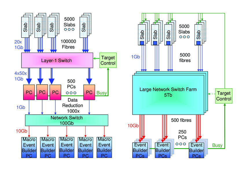
Standard Configuration
In our assumed standard detector configuration, communication from the VFE will pass
via the electronics at the FE to an off-detector receiver. We assume that threshold
suppression will be done at the FE, and hence the rate would be significantly
reduced from that at the VFE. Assuming that the rate is reduced to 1% of the
original data volume of 250 GBytes per bunch train and each sample above threshold
needs a channel and timing label, the total data volume to be read out from the
calorimeter is about 5 GBytes or about 1 MByte per slab. These data have to be
read out within a bunch train period of 250 ms, giving a rate of 5 MBytes/s.
Alternative configuration
Here we imagine that the FE is removed and the communication is directly from the
VFE to the off-detector. We assume that the ASIC only digitises the data and
250 GBytes has to be transported off the detector per bunch train. This will
require a high-speed optical network. It should be noted, however, that the need for
FE electronics also becomes questionable if more processing is done on the ASIC chip,
such as threshold suppression. In such a scenario, transporting the data directly
from the ASIC off the detector could be done and so the FE would become redundant.
The number of fibres required to read-out the 24 million channels would vary between
750 000 to about 90 000 depending on whether the ASIC handles 32 or 256 channels.
If we assume that the diameter of a fibre is 150 m, or with cladding
250 m then if half of the circumference of 12 m had fibres running along it,
the bundle would be up to 1 cm in depth, but could be as little as 1 mm, depending
on the number of ASICs and hence fibres. This would leave ample room for other cables
and power supplies. This concept would revolutionise the whole calorimeter design and
so needs to be considered now when changes in its general structure could be
considered. Our research in this area will provide important feedback to groups
designing the ASIC chips.
The off-detector receiver, as described later, is assumed to consist of PCI cards housed in PCs. The reliability of large PC farms is an issue for reading out the data; if one PC goes down, all of the data in that region of the calorimeter is lost. Current PC farms show a rate of 1 PC failure per day in a farm of 200. This is not large but is also not small and would require some surplus of PCs (say 10%) above the number required based just on the number of detector channels. For a final working calorimeter readout system these PCs would need to be repaired and put back into the system on a regular basis. The standard scenario would require less high-speed equipment off the detector, whereas the alternative would require many optical fibres with dedicated optical switching. The alternative scenario would, however, remove material from inside the detector which would ease construction and have a potentially advantageous impact on event reconstruction and, hence, physics measurements. It would also reduce the number of processing components within the detector which could be attractive since they would be inaccessible for long periods of time.
Using the experience gained from the two scenarios above, a hybrid path can be explored. By optimising the functionality in the VFE and matching it to an FE, overall instantaneous data rates can be reduced as well as lowering fibre count. For example, if data is buffered in the VFE, some form of passive multiplexer can be envisaged that will combine data from all the VFEs. This could take the form of spliced optic-fibres, or an OR gate. This would not necessarily remove the need for an FE, but the reduced size and complexity will have many benefits (thermal, configuration time, SEUs, cost, etc.).
To transmit data onto the detector, we will attempt to use the same commercial hardware used for off-detector communication. The requirements are different, though, as the detector front-end requires clock and synchronisation signals as well as low-level configuration and data signals. Commercial network hardware is not ideally suited to synchronous tasks but the significant cost and reliability benefits make it worthy of investigation. This is split into two areas: failsafe configuration prior to normal running, and clock and control signal distribution.
Failsafe Configuration In a scenario requiring an FPGA on-detector, it is imperative that the device can be re-configured remotely. This is necessary not only because of the number of FPGAs but also because of the uncertainty in the detector performance in terms of data suppression, pedestal drifts, bad channel identification etc., all of which have to be implemented in the FE FPGA. The optimal algorithms for these tasks will only be determined after some experience of operating the calorimeter. As the FPGAs are relatively inaccessible, it is important that a failsafe method of reseting and re-configuring the devices exists.
Avoiding the use of additional control lines necessitates a means to extract signals from the communications interface. Most probably this will involve “spying” on the serial data line.
Of primary importance is to force the FPGA into a known state under any conditions (i.e. a hard-reset). It may simply be possible to send an exceptionally long series of “1”s to the slab (say 40M = 1 second) where an RC type-circuit with a long time-constant will trigger the reset. A more complex method would require some discrete logic (like a shift-register with parallel output into a comparator) searching the incoming data-stream for a “magic” number. Power cycling the board is also a (less elegant) solution, but still requires attention in circuit design to ensure the FPGA will boot.
Once hard-reset, the FPGA will follow its start-up logic to initiate the boot - making use of 2 distinct methods:
-
•
Use a non-volatile base configuration that is either hardwired into the FPGA or provided by a EEPROM external to the FPGA. In this case the FPGA would assist in writing the configuration to its internal RAM and then issue a re-boot-using-internal-configuration command to itself.
-
•
By waiting for external stimulus (usually a clock) to control data the data being fed into the device. This requires additional hardware to format the the serial-data into data/clock/control for FPGA consumption.
In both cases some external hardware is required, the amount of which will only fully understood after a more detailed evaluation. A possible outcome could be that a small non-volatile programmable device could provide the most flexible solution, but the effects of radiation need further examination.
Larger devices with non-volatile configuration memories could be used for the entire front-end logic, but apart from the increased cost and limited re-programming cycles making these less desirable, these devices are not able to re-program themselves.
Reliability in the detector environment of these memories over the lifetime of an experiment, as well as SEUs, also need to be addressed. Non-volatile memories have limited programming cycles, whereas modern SRAM-based FPGAs boast that they can re-configured an infinite number of times. By refreshing the configuration periodically, the effect of SEU corruption can be minimised. Considering an FPGA with one million logic gates (which specifies a 4 Mbit PROM), configuring this device at 40 MHz would take 100 ms - a re-config every 250 ms bunch-train!
Being able to re-configure the FE when needed also allows the selection of a smaller component that can be configured for specific function, rather than a large one-size fits all device.
Reducing the number of components on the front-end-module is advantageous from a cost, reliability and dead material point of view, so we will focus on methods of generating a data-stream onto the detector that requires the minimum of components to extract signals from the physical network interface module.
Clock and Control To ensure the on-detector electronics captures data from actual collisions, all components in the detector are synchronised to the bunch-crossing clock. Bunch-train start, stop and ID signals are also be required. Traditionally this is done with a bespoke, low-latency, highly synchronous system, but here we will look at using a commercial network switch.
Switches are not designed for synchronous signal fanout. In fact the now obsolete forerunner to the switch, the hub, is much better suited to the task. Modes for signal broadcasting do exist, but these need to be closely examined. Studies on latency and port-to-port skew will be undertaken.
To obtain maximal control over timing, the lowest level protocols will need to be used. Directly accessing the network at the physical layer (i.e. as a simple serial link) would facilitate complete control over data-packet composition and timing. For this a specialist and customisable network interface card is required.
To regenerate the clock at the detector end, the time structure of the data transmitted needs to be structured accordingly. This would probably take the form of a local oscillator being periodically resynced to the data clock. As the bunch-crossing interval is 7 ns, a 1 Gbit (1 ns) link would be the minimum rate needed. Board-level signals, such as train-start may also need to be decoded directly from the data stream (as with the failsafe system above).
In summary, this is as an investigation to verify that a clock, control and configuration system can be constructed using commercial network hardware for distribution.
3.3 Off-detector receiver
An ideal system would have all data from the detector for each bunch train sent directly to a single PC where full event reconstruction would be performed. However, considering that the electromagnetic calorimeter alone will contain 24 million channels, even after data suppression this seems unfeasible.
It would, however, be desirable to geographically group as many channels as possible at a processor. This would permit broader local clustering which could be used as an input to full event reconstruction later. The fundamental questions to be answered are how much of the calorimeter can be received into one PC and how much needs to be received to make local clustering effective. The impact this has on full event reconstruction and on simulated physics needs to be evaluated. This task therefore involves a combination of hardware and simulation work.
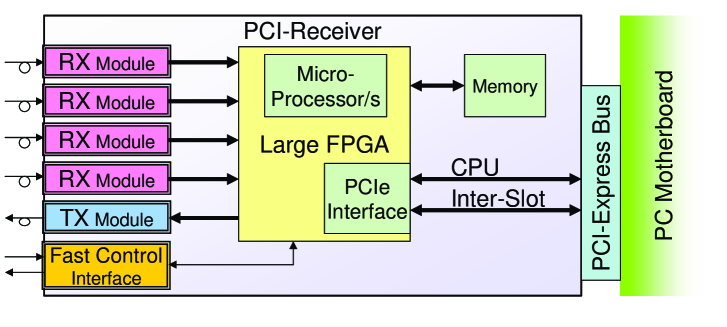
We propose a system comprising PCI cards (see Fig. 4) mounted in PCs. These cards will provide timing, clock, control and configuration data, be capable of performing local clustering, as well as being able to be re-configured to act as data transmitters to exercise the receivers. We will use the “new” PCI Express bus standard [9] as this offers increased bandwidth and flexibility by using many high bandwidth serial links (called lanes) instead of a single parallel bus. It is expected to be scalable due to future increases in the number of lanes. Aside from providing an interface to the processor, lanes can be setup between cards, allowing advanced clustering prior to processing.
Although it is hard to predict what technology will be available for the final system, gaining experience with serial bus technologies now, will prove valuable for estimates of how much data can be realistically processed by a computer and help us understand the benefits and bottlenecks, as well as the scalability.
Much of this DAQ workpackage relies on novel methods in using network infrastructure, so a card providing both direct access to the network hardware and room to build any other functionality is useful. This applies to the PCI Express interface too, where the card will be able to test-drive the bus and provide debug feedback and monitoring.
4 A model DAQ system for the ECAL
As has been discussed in this note many options exist for the functionality of the components at various stages. It is therefore difficult to make a definitive statement on what a DAQ system would like and how many components it would have. However, work is ongoing to try and do as much of the work (data reduction) as possible on the detector, thereby reading out as little as possible. Therefore we consider that the ADC and thresholding are done in a 32-channel VFE and buffering in the FE. Under this model and making reasonable assumptions on the data rate a model system is detailed below.
The raw data size is assumed to be 2 Bytes per channel with an additional 4 Bytes per channel needed for a timing label. Imposing the threshold suppression reduces the data rate by a factor of 100, leading to a data size for the whole detector of ( 7.0 GBytes. The size per slab is then 1.1 MBytes. As the data is buffered in the FE, it is read out between bunch trains giving a rate per slab of 4.7 MBytes/s. Early testing will readout some slabs individually, but as the system grows and stabilises, it would clearly be advantageous to bundle the data from several slabs together. Bundling half a tower of 20 slabs would give a rate of 0.75 Gbit/s which could be adequately read out using current fibres. Such a grouping would lead to 300 fibres coming off the detector. Assuming a PCI card which can receive 8 fibres, this would require 38 PCI cards. With a PC hosting 2 such cards than a system of 19 PCs would be required. We then assume a 20% contingency for more fibres reading out neighbouring areas to allow for redundancy and for faulty PCs or PCI cards. This gives a total of about 50 PCI cards housed in 25 PCs a clearly manageable number for such a granular calorimeter.
5 Summary
A conceptual design of a data acquisition system for the ILC calorimeter has been discussed. The concept relies heavily on commercial equipment and is generic such that it could be applied to other detector systems. Potential bottlenecks have been identified and form a programme of research and development of the next three to four years for the CALICE-UK groups. Bench tests and real-time tests with prototype calorimeters, within the EUDET project, will be undertaken. After this period, a technical design of the data acquisition system will be possible.
References
- [1] TESLA: The superconducting Electron-Positron Linear Collider with an integrated X-Ray Laser Laboratory. Technical Design Report. DESY 2001-011. March 2001.
-
[2]
LDC Outline Document (2006)
http://www.ilcldc.org/documents/dod/outline.pdf -
[3]
SiD Outline Document (2006)
http://hep.uchicago.edu/oreglia/siddod.pdf - [4] CALICE-UK: Proposal 317 - The CALICE collaboration: calorimeter studies for a future linear collider.
- [5] www.eudet.org
- [6] C. De La Taille, VFE electronics design group, private communication.
- [7] http://www.intel.com/update/contents/it04041.htm
- [8] http://www.xilinx.com/xlnx/xil_prodcat_landingpage.jsp?titleVirtex-4
-
[9]
http://www.intel.com/update/contents/st11041.htm?iid=labs_homepage+update_st11041&
http://www.intel.com/technology/pciexpress/downloads/pci_ei_pcb_guidelines.pdf - [10] P.D. Dauncey et al., “MAPS conceptual design”, LC Note in preparation.
- [11] J.Fleury, et al., “Front End Electronics for Si-W Calorimeter,” proceedings of the LCWS04 Conference, Paris, April 2004.