physics/0611272
Radiation Hardness of CCD Vertex Detectors
for the ILC
André Sopczak1,
Khaled Bekhouche2,
Chris Bowdery1,
Chris Damerell3,
Gavin Davies1,
Lakhdar Dehimi2,
Tim Greenshaw4,
Michal Koziel1,
Konstantin Stefanov3,
Tim Woolliscroft4,
Steve Worm3
1Lancaster University, U.K.
2LMSM Laboratory Biskra University, Algeria
3CCLRC Rutherford Appleton Laboratory (RAL), U.K.
4Liverpool University, U.K.
Abstract
Abstract
Results of detailed simulations of the charge transfer inefficiency of a prototype CCD chip are reported. The effect of radiation damage in a particle detector operating at a future accelerator is studied by examining two electron trap levels, 0.17 eV and 0.44 eV below the bottom of the conduction band. Good agreement is found between simulations using the ISE-TCAD DESSIS program and an analytical model for the 0.17 eV level. Optimum operation is predicted to be at about 250 K where the effect of the traps is minimal which is approximately independent of readout frequency. This work has been carried out within the Linear Collider Flavour Identification (LCFI) collaboration in the context of the International Linear Collider (ILC) project.
I Introduction
Particle physicists worldwide are working on the design of a high energy collider of electrons and positrons (the International Linear Collider or ILC) which could be operational sometime after 2016. Any experiment exploiting the ILC will require a high performance vertex detector to detect and measure short-lived particles. One candidate for such a device would consist of a set of concentric cylinders of charge-coupled devices (CCDs).
An important requirement of a vertex detector is to remain tolerant to radiation damage for its anticipated lifetime.
CCDs suffer from both surface and bulk radiation damage. However, when considering charge transfer losses in buried channel devices only bulk traps are important. These defects create energy levels between the conduction and valence band, hence electrons may be captured by these new levels. These electrons are also emitted back to the conduction band after a certain time. For a signal packet this may lead to a decrease in charge as it is transferred to the output and may be quantified by its Charge Transfer Inefficiency (CTI), where a charge of amplitude transported across pixels will have a reduced charge given by
| (1) |
The CTI value depends on many parameters, some related to the trap characteristics such as: trap energy level, capture cross-section, and trap concentration (density). Operating conditions also affect the CTI as there is a strong temperature dependence on the trap capture rate and also a variation of the CTI with the readout frequency. Other factors are also relevant, for example the occupancy ratio of pixels, which influences the fraction of filled traps in the CCD transport region. Previous studies have been reported [1, 2, 3, 4, 5].
II SIMULATIONS
The UK Linear Collider Flavour Identification (LCFI) collaboration [6, 7] has been studying a device produced by e2V Technologies, with a manufacturer’s designation ‘CCD58’. It is a 2.1 Mpixel, three-phase buried-channel CCD with 12 m square pixels.
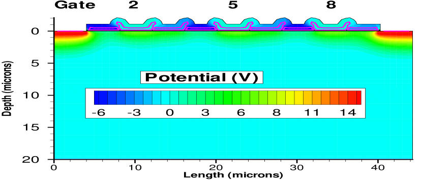
Simulations of a simplified model of this have been performed with the ISE-TCAD package (version 7.5), particularly the DESSIS program (Device Simulation for Smart Integrated Systems). It contains an input gate, an output gate, a substrate gate and nine further gates (numbered 1 to 9) which form the pixels. Each pixel consists of 3 gates but only one pixel is important for this study—gates 5, 6 and 7. The simulation is essentially two dimensional but internally there is a nominal 1 m device thickness (width). This is equivalent to a thin slice of the device with rectangular pixels 12 m long by 1 m wide. The overall length and depth of the simulated device are 44 m and 20 m respectively (Fig. 1).
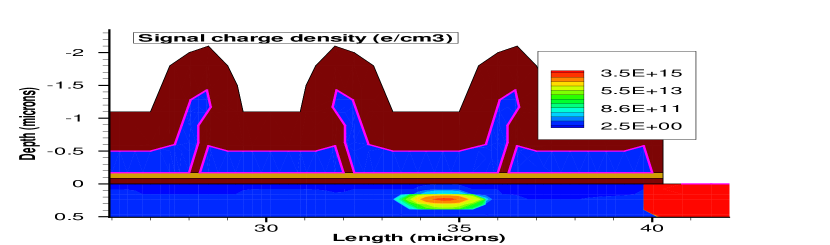
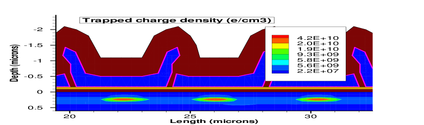
Parameters of interest are the readout frequency, up to 50 MHz, and the operating temperature between 120 K and 300 K although simulations have been done up to 500 K. The charge in transfer and the trapped charge are shown in Fig. 2.
The signal charge used in the simulation is chosen to be similar to the charge generated by a minimum ionising particle (MIP), amounting to about 1620 electron-hole pairs111This number has to be divided by 12 because the charge is assumed to be distributed over the whole pixel but the model has only 1/12th of the true pixel volume. for CCD58. DESSIS has a directive for generating heavy ions and this is exploited to create the charges. The heavy ion is made to travel in a downwards direction starting at 1.2 m below gate 2 at 1 s before charge transfer begins. This provides ample time for the electrons to be drawn upwards to the transport channel which is 0.25 m beneath the gate electrodes.
II-A Calculating CTI
Charge Transfer Inefficiency is a measure of the fractional loss of charge from a signal packet as it is transferred over a pixel, or three gates. After DESSIS has simulated the transfer process, a 2D integration of the trapped charge density distribution is performed independently to give a total charge under each gate.
The CTI for transfer over one gate is equivalent to
| (2) |
where:
-
•
= electron signal packet density,
-
•
= background trapped electron charge density prior to signal packet transfer,
-
•
= trapped electron charge density under the gate, after signal transfer across gate.
In this way the CTI is normalised for each gate. The determinations of the trapped charge take place for gate when the charge packet just arrives at gate . If the determination were made only when the packet has cleared all three gates of the pixel, trapped charge may have leaked out of the traps.
The total CTI (per pixel) is determined from gates 5, 6 and 7, hence
| (3) |
where is the gate number. The background charge is taken as the trapped charge under gate 2 because this gate is unaffected by the signal transport when the charge has just passed gates being processed.
II-B Initial tests of the DESSIS program
DESSIS simulations have been carried out with a zero concentration of electron traps as in unirradiated silicon.
The DESSIS program is steered with a command file which contains electrode voltage values for each of the three phases as a function of time. For these simulations the voltage values (peak value 7 V), which were originally digitised from real experiments with CCD58, were replaced by reduced values without altering the frequency or phase.
Since there were no traps there was no trapped charge so a different estimator of CTI is required. The electron charge density left under gate when the charge packet has moved to gate gives the partial CTI estimator. It is normalised by the original electron charge density. As before, the CTI for a pixel is computed by adding the partial CTI’s for gates 5, 6, and 7.
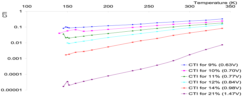
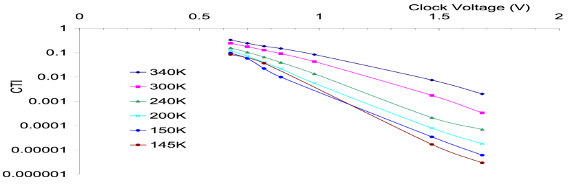
Figure 3 shows the variation of CTI with temperature for various clock voltages. Figure 4 shows the variation of CTI with clock voltage for a range of temperatures. The device operates with a negligible CTI above 3 V and has a large CTI below 1 V. Also the CTI grows with temperature.
Examination of snapshots of electron density plots produced by DESSIS during a simulation run confirm that electrons leak out of the main charge packet during transfer at reduced clock voltages leading to an even distribution of electrons under all of the gates.
II-C 0.17 eV and 0.44 eV traps
This CTI study, at nominal clock voltage, focuses only on the bulk traps with energies 0.17 eV and 0.44 eV below the bottom of the conduction band. These will be referred to simply as the 0.17 eV and 0.44 eV traps. An incident particle with sufficient energy is able to displace an atom from its lattice point leading eventually to a stable defect. These defects manifest themselves as energy levels between the conduction and valence band, in this case the energy levels 0.17 eV and 0.44 eV; hence electrons and/or holes may be captured by these levels. The 0.17 eV trap is an oxygen vacancy defect, referred to as an A-centre defect. The 0.44 eV trap is a phosphorus-vacancy defect—an E-centre defect—that is, a result of the silicon being doped with phosphorus and a vacancy manifesting from the displacement of a silicon atom bonded with the phosphorus atom [2].
In order to determine the trap densities for use in simulations, a literature search on possible ILC radiation backgrounds and trap induction rates in silicon was undertaken. The main expected background arises from e+e- pairs with an average energy of 10 MeV and from neutrons (knocked out of nuclei by synchrotron radiation).
Table 1 shows results of background simulations of e+e- pairs generation for three proposed vertex detector designs (from three ILC detector concepts).
| Simulator | SiD | LDC | GLD |
|---|---|---|---|
| CAIN/Jupiter | 2.9 | 3.5 | 0.5 |
| GuineaPig | 2.3 | 3.0 | 2.0 |
Table 1. Simulated background results for three different detector scenarios. The values are hits per square centimetre per e+e- bunch crossing. SiD is the Silicon Detector Concept [8], LDC is the Large Detector Concept [9] and GLD is the Global Linear collider Detector [10].
Choosing the scenario with the highest expected background, that is the LDC concept, where the innermost layer of the vertex detector would be located 14 mm from the interaction point, one can estimate an e+e- flux around 3.5 hits/cm2/bunch crossing which gives a fluence of 0.5 e/cm2/year. In the case of neutrons, from two independent studies, the fluence was estimated to be 1010 n/cm2/year [11] and 1.6 n/cm2/year [12].
Based on the literature [13, 14, 15, 16, 17, 18, 19, 20, 21], the trap densities introduced by 1 MeV neutrons and 10 MeV electrons have been estimated with two established assumptions: the electron trap density is a linear function of dose, and the dose is a linear function of fluence. A summary is given in Table 2.
| Particle type | 0.17 eV () | 0.44 eV () |
|---|---|---|
| 10 MeV e- | ||
| 1 MeV n | ||
| total |
Table 2. Estimated densities of traps after irradiation for one year. For neutrons, the literature provides two values.
The actual trap concentrations and electron capture cross-sections used in the simulations are shown in Table 3.
| (eV) | Type | () | () |
|---|---|---|---|
| 0.17 | Acceptor | ||
| 0.44 | Acceptor |
Table 3. Trap concentrations (densities) and electron capture cross-sections as used in the DESSIS simulations.
II-D Partially Filled Traps
Each electron trap in the semiconductor material can either be empty (holding no electron) or full (holding one electron). In order to simulate the normal operating conditions of CCD58, partial trap filling was employed in the simulation (which means that some traps are full and some are empty) because the device will transfer many charge packets during continuous operation.
In order to reflect this, even though only the transfer of a single charge packet was simulated, the following procedure was followed in all cases. From t = 0 seconds to t = 98 s, the gates ramp up and are biased in such a way to drain the charge to the output drain. The device is in a fully normal biased state then at 98 s. To obtain partial trap filling, the simulation waits222This waiting time is calculated from a 1% mean pixel occupancy with a 50 MHz readout frequency. 2 s between 98 s and 100 s to allow traps to partially empty. The test charge is generated at 99 s. The simulation then starts the three clock phases, varying voltage with time to cause the transfer of the signal charge packet through the device.
III Analytical Models
The motivation for introducing the following two simple analytical models is to understand the underlying effects and to make comparisons with the DESSIS simulations (referred to as the “full simulations”).
III-A Simple CTI Model
Firstly, a simple analytical model is considered, based upon a single trapping level—a so-called Simple CTI model. This is significantly faster than a full simulation. It also provides a simple method to see the effect of changing parameters and demonstrates physics understanding.
The charge transfer process is modelled by a differential equation in terms of the different time constants and temperature dependence of the electron capture and emission processes. In the electron capture process, electrons are captured from the signal packet and each captured electron fills a trap. This occurs at the capture rate . The electron emission process is described by the emission of captured electrons from filled traps back to the conduction band, and into a second signal packet at the emission rate .
III-A1 Capture and emission time constants
The Shockley-Read-Hall theory [22] considers a defect at an energy below the bottom of the conduction band, , and gives
| (4) | |||||
| (5) |
where:
-
•
= electron capture cross-section
-
•
= entropy change factor by electron emission
-
•
= electron thermal velocity
-
•
= density of states in the conduction band
-
•
= Boltzmann’s constant
-
•
= absolute temperature
-
•
= density of signal charge packet.
It is assumed that .
At low temperatures, the emission time constant can be very large and of the order of seconds. The charge shift time is of the order of nanoseconds. A larger means that a trap remains filled for much longer than the charge shift time. Further trapping of signal electrons is not possible and, consequently, CTI is small at low temperatures. A peak occurs between low and high temperatures because the CTI is also small at high temperatures. This manifests itself because, at high temperatures, the emission time constant decreases to become comparable to the charge shift time. Now, trapped electrons rejoin their signal packet.
III-A2 Charge Transfer Equation
From the fraction of filled traps, the following differential equation can be derived:
| (6) |
where is the time-dependent fraction of filled traps
| (7) |
-
•
= density of traps filled by electrons
-
•
= density of traps
Considering that the traps are partially filled and using the initial condition:
| (8) |
where is the fraction of filled traps after a mean waiting time, , the differential equation can be solved to provide an expression for the CTI:
| (9) |
| (10) |
| (11) |
where is the shift-time. For one gate, , where is the readout frequency.
This definition is for CTI for a single trap level. The factor of three appears since there is a sum over the three gates that make up a pixel.
III-A3 Matching the CTI definition of the simulation
The Simple Model has been adapted by including initially filled traps and by the incorporation of a so-called factor to CTI:
| (12) |
This models the situation where the trapped charge under gate 5 started to empty at time minus three shift-times, that under gate 6 at minus two shift-times and that under gate 7 at minus one shift-time. An alternative factor, called , has also been used to compare with simulated data. This is defined as:
| (13) |
and models the situation one shift-time earlier than for .
III-B Improved Model
The second analytical model that has been developed is referred to as the Improved Model (IM), based on the work of T. Hardy et al. [23]. It is improved by adjusting initial assumptions to fit the study of CCD58. The Improved model also considers the effect of a single trapping level, but only includes the emission time in its differential equation:
| (14) |
where is the density of filled traps. The traps are initially filled for this model and . Nevertheless, to be consistent with the full DESSIS simulations (that use partially filled traps) the Improved Model uses a time constant between the filling of the traps such that the traps remain partially filled when the new electron packet passes through the CCD. The solution of this differential equation leads to another estimator of the CTI:
| (15) |
-
•
is the total emission time from the previous packet.
-
•
is the time period during which the charges can join the parent charge packet.
IV Simulation Results
The CTI dependence on temperature and readout frequency was explored using ISE-TCAD simulations.
IV-1 0.17 eV traps
Figure 5 shows the CTI for simulations with partially filled 0.17 eV traps at different frequencies for temperatures between 123 K and 260 K, with a nominal clock voltage of 7 V.
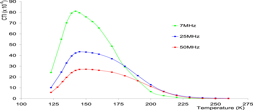
A peak structure can be seen. For 50 MHz, the peak is at 150 K with a CTI of . The peak CTI is in the region between 145 K and 150 K for a 25 MHz clock frequency and with a value of about . This is about 1.6 times bigger than the charge transfer inefficiency at 50 MHz. The peak CTI for 7 MHz occurs at about 142 K, with a maximum value of about , an increase from the peak CTI at 50 MHz by a factor of about 3 and an increase from the peak CTI at 25 MHz by a factor of nearly 2. Thus CTI increases as frequency decreases. For higher readout frequency there is less time to trap the charge, thus the CTI is reduced. At high temperatures the emission time is so short that trapped charges rejoin the passing signal.
IV-2 0.44 eV traps
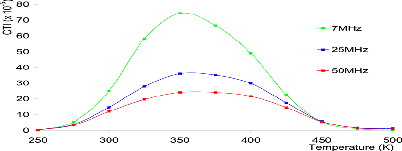
Simulations were also carried out with partially filled 0.44 eV traps at temperatures ranging from 250 K to 500 K. This is because previous studies [5] on 0.44 eV traps have shown that these traps cause only a negligible CTI at temperatures lower than 250 K due to the long emission time and thus traps remain fully filled at lower temperatures. The results are depicted in Fig. 6.
The peak CTI is higher for lower frequencies with little temperature dependence of the peak position.
IV-3 0.17 eV and 0.44 eV traps together
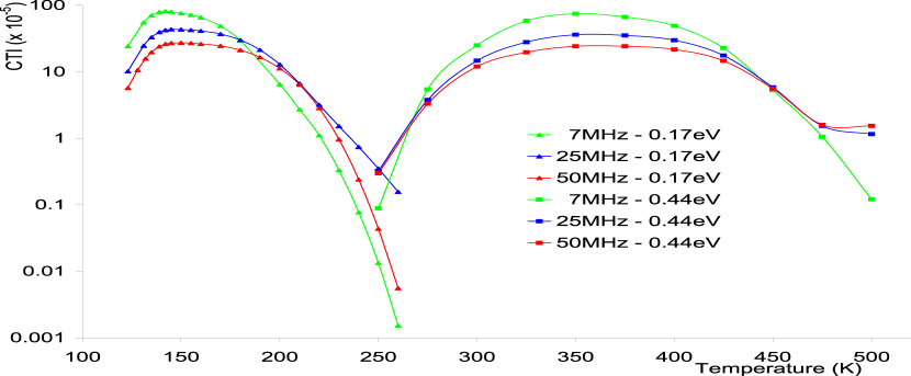
The logarithmic scale view (Fig. 7) of the simulation results at the different frequencies and trap energies clearly identifies an optimal operating temperature of about 250 K.
IV-A Comparisons with Models
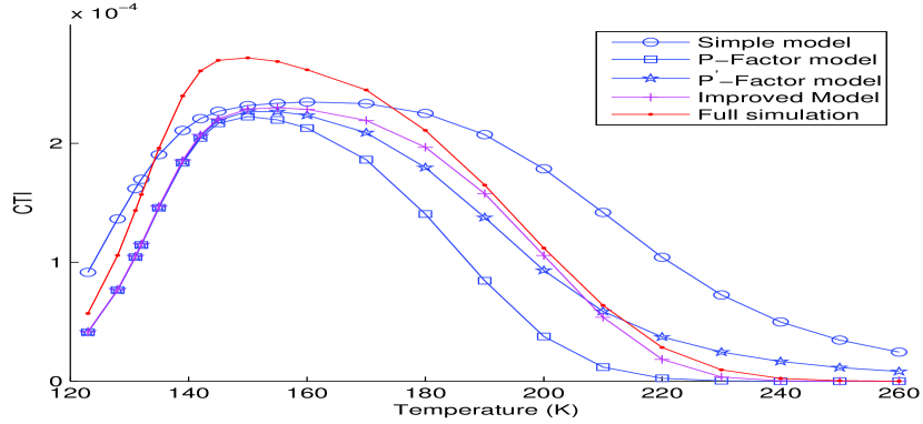
Figure 8 shows that the basic Simple Model does not agree well with the full simulation. Applying the factor appears to overcompensate for the deficiencies and the factor gives a reasonable but not perfect agreement.
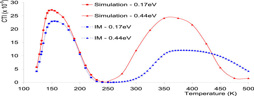
Figure 9 compares the full DESSIS simulation for 0.17 eV and 0.44 eV traps and clocking frequency of 50 MHz to the Improved Model. It emphasises the good agreement between the model and full simulations at temperatures lower than 250 K with 0.17 eV traps, but shows a disagreement at higher temperatures for the 0.44 eV traps.
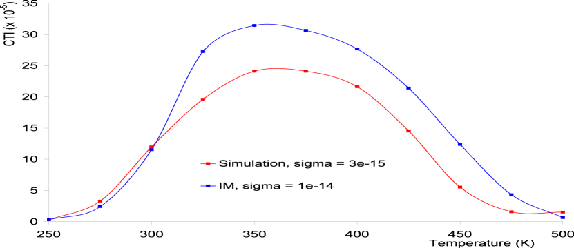
If the 0.44 eV trap electron capture cross-section in the Improved Model is increased to cm2, a somewhat better agreement is found, as shown in Figure 10. However it is clear that there are limitations with the Improved Model. They could relate to a breakdown of the assumptions at high temperatures, to ignoring the precise form of the clock voltage waveform, or to ignoring the pixel edge effects. Further studies are required.
V Conclusions
The Charge Transfer Inefficiency (CTI) of a CCD device has been studied with a full simulation (ISE-TCAD DESSIS) and compared with analytical models.
Partially filled traps from the 0.17 eV and 0.44 eV trap levels have been implemented in the full simulation and variations of the CTI with respect to temperature and frequency have been analysed. The results confirm the dependence of CTI with the readout frequency. At low temperatures ( K) the 0.17 eV traps dominate the CTI, whereas the 0.44 eV traps dominate at higher temperatures.
A large emission time constant results in a trap remaining filled for much longer than the charge shift time. Further trapping of signal electrons is not possible so the CTI is small at low temperatures. At high temperatures the emission time constant decreases to become comparable to the charge shift time. Trapped electrons rejoin their signal packet and, because most are emitted during the charge transfer time, there is again a small CTI. For intermediate temperatures, a clear peak structure is observed.
Good agreement between simulations and a so-called Improved Model has been found for 0.17 eV traps but not for 0.44 eV traps. This shows the limitations of the Improved Model with respect to the full simulation.
The optimum operating temperature for CCD58 in a high radiation environment is found to be about 250 K.
Interest is now moving to alternative CCD designs, particularly 2-phase column-parallel readout devices. The extensive amount of research that has been carried out on CCD58 contributes to the development of future CCD designs.
Acknowledgments
This work is supported by the Particle Physics and Astronomy Research Council (PPARC) and Lancaster University. The Lancaster authors wish to thank Alex Chilingarov, for helpful discussions, and the particle physics group at Liverpool University, for the use of its computers.
References
-
[1]
J.R. Janesick, “Scientific Charge-Coupled Devices”, SPIE Press, ISBN 0819436984 (2001).
-
[2]
K. Stefanov, PhD thesis, Saga University (Japan),
“Radiation damage effects in CCD sensors for tracking applications
in high energy physics”, 2001, and references therein;
K. Stefanov et al., IEEE Trans. Nucl. Sci., 47 (2000) 1280.
-
[3]
O. Ursache, Diploma thesis, University of Siegen (Germany),
“Charge transfer efficiency simulation in CCD for application as
vertex detector in the LCFI collaboration”, 2003, and references therein.
-
[4]
J.E. Brau, O. Igonkina, C.T. Potter and N.B. Sinev,
Nucl. Instr. and Meth. A549 (2005) 117;
J.E. Brau and N.B. Sinev, IEEE Trans. Nucl. Sci. 47 (2000) 1898.
-
[5]
A. Sopczak, “LCFI Charge Transfer Inefficiency Studies for CCD
Vertex Detectors”,
IEEE 2005 Nuclear Science Symposium, San Juan, USA, Proc. IEEE Nuclear Science Symposium
Conference Record, N37-7 (2005) 1494;
A. Sopczak, “LCFI Charge Transfer Inefficiency Studies for CCD Vertex Detectors”, 9th ICATPP Conference on Astroparticle, Particle, Space Physics, Detectors and Medical Physics Applications, Como, Italy, Proc. World Scientific (Singapore) p. 876;
A. Sopczak, “Charge Transfer Efficiency Studies of CCD Vertex Detectors”, on behalf of the LCFI collaboration, Int. Linear Collider Workshop, LCWS’05, Stanford University, USA, physics/0507028, Proceedings p. 544.
-
[6]
LCFI collaboration homepage:
http://hepwww.rl.ac.uk/lcfi/
-
[7]
S.D. Worm, “Recent CCD developments for the vertex detector of
the ILC - including ISIS (In-situ Storage Image Sensors)”, 10th
Topical Seminar on Innovative Particle and Radiation Detectors
(IPRD06) 1–5 October, 2006, Siena, Italy;
T.J. Greenshaw, “Column Parallel CCDs and In-situ Storage Image Sensors for the Vertex Detector of the International Linear Collider”, 2006 Nuclear Science Symposium, October 29–November 4, 2006, San Diego, USA.
-
[8]
SiD collaboration homepage: http://www-sid.slac.stanford.edu/
-
[9]
LDC collaboration homepage: http://www.ilcldc.org/
-
[10]
GLD collaboration homepage: http://ilcphys.kek.jp/gld/
-
[11]
Private communication from Takahi Maruyama, Stanford Linear
Accelerator Center (SLAC), 2006.
-
[12]
A. Vogel, private communication (DESY Hamburg), 2006.
-
[13]
M.S. Robbins “The Radiation Damage Performance of Marconi
CCDs” Marconi Technical Note S&C 906/424 2000 (unpublished).
-
[14]
M.S. Robbins et al., IEEE Trans. Nucl. Sci. 40 (1993) 1561.
-
[15]
M.S. Robbins, T. Roy and S.J. Watts, Proceedings of the First European Conference on
Radiation and its Effects on Devices and Systems, RADECS 91,
ISBN: 0-7803-0208-7 (1992) 327.
-
[16]
J.W. Walker and C.T. Sah, Phys. Rev. B7 (1972) 4587.
-
[17]
G.K. Wertheim, Phys. Rev. 110 (1958) 1272.
-
[18]
M. Suezawa, Physica B340-342 (2003) 587.
-
[19]
N.S. Saks, IEEE Trans. Nucl. Sci. 24 (1977) 2153.
-
[20]
J.R. Srour, R.A. Hartmann and S. Othmer, IEEE Trans. Nucl. Sci. 27 (1980) 1402.
-
[21]
E. Fretwurst et al., Nucl. Instr. and Meth. A377 (1996) 258.
-
[22]
W. Shockley and W.T. Read, Phys. Rev. 87
(1952) 835;
R.N. Hall, Phys. Rev., 87 (1952) 387.
-
[23]
T. Hardy, R. Murowinski and M.J. Deen, IEEE Trans.
Nucl. Sci. 45 (1998) 154.
-
[24]
C. Rimbault et al., Phys. Rev. ST Accel. Beams 9 (2006) 034402.
-
[25]
C. Rimbault, “Study of incoherent pair e+e- background in the
Vertex Detector with GuineaPig”, 2005 International Linear Collider
Physics and Detector Workshop and Second ILC Accelerator Workshop
Snowmass, Colorado, August 14-27, 2005.
-
[26]
T. Maruyama
“Backgrounds” , 2005 International Linear Collider Physics and
Detector Workshop and Second ILC Accelerator Workshop, Snowmass,
Colorado, August 14-27, 2005.