Constriction-limited detection efficiency of superconducting nanowire single-photon detectors
Abstract
We investigate the source of large variations in the observed detection efficiencies of superconducting nanowire single-photon detectors between many nominally identical devices. Through both electrical and optical measurements, we infer that these variations arise from “constrictions:” highly localized regions of the nanowires where the effective cross-sectional area for superconducting current is reduced. These constrictions limit the bias current density to well below its critical value over the remainder of the wire, and thus prevent the detection efficiency from reaching the high values that occur in these devices only when they are biased near the critical current density.
pacs:
74.76.Db, 85.25.-jSuperconducting nanowire single-photon detectors (SNSPDs) newtech ; newsob ; inductance ; cavity provide a unique combination of high infrared detection efficiency (up to 57% at 1550nm cavity has been demonstrated) and high speed (30 ps timing resolution newsob ; ASCeric , and few-ns reset times after a detection event inductance ). Applications for these devices already being pursued include high data-rate interplanetary optical communications comm , spectroscopy of ultrafast quantum phenomena in biological and solid-state physics nistfiber ; qspec , quantum key distribution (QKD) QKD , and noninvasive, high-speed digital circuit testing CMOS .
In many of these applications, large arrays of SNSPDs would be extremely important ASCeric . For example, existing SNSPDs have very small active areas, making optical coupling relatively difficult and inefficient nistfiber ; sobfiber . Their small size also limits the number of optical modes they can collect, which is critical in free-space applications where photons are distributed over many modes, such as laser communication through the atmosphere (where turbulence distorts the optical wavefront) and in fluorescence detection. Furthermore, it was shown in Ref. inductance that the maximum count rate for an individual SNSPD decreases as its active area is increased, due to its kinetic inductance, forcing a tradeoff between active area and high count rates. Count rate limitations are particularly important in optical communications and QKD, affecting the achievable receiver sensitivity or data rate comm ; twoelement . Detector arrays could provide a solution to these problems, giving larger active areas while simultaneously increasing the maximum count rate by distributing the flux over many smaller (and therefore faster) pixels. Large arrays could also provide spatial and photon-number resolution. Although few-pixel detectors have been demonstrated ASCeric ; twoelement ; QKD ; sobfiber , fabrication and readout methods scalable to large arrays have not yet been discussed.
A first step towards producing large arrays of SNSPDs is to understand (and reduce) the large observed variation of detection efficiencies for nominally identical devices cavity , which would set a crippling limit on the yield of efficient arrays of any technologically interesting size. In this Letter, we demonstrate that these detection efficiency variations can be understood in terms of what we call “constrictions:” highly localized, essentially pointlike regions where the nanowire cross-section is effectively reduced, and which are not due to lithographic patterning errors (line-edge roughness).
The electrical operation of these detectors has been discussed previously by several authors newtech ; newsob ; inductance ; cavity ; joelmodel , so we only summarize it here. The NbN nanowires are biased with a DC current slightly below the critical value . An incident photon of sufficient energy can produce a resistive “hotspot” which in turn disrupts the superconductivity across the wire, producing a series resistance which then expands in size due to Joule heating inductance ; joelmodel . The series resistance quickly becomes 50, and the current is diverted out of the device and into the 50 transmission line connected across it, resulting in a propagating voltage pulse on the line. The device can then cool back down into the superconducting state, and the current through it recovers with the time constant , where is the kinetic inductance inductance .
The nanowires used in this work were patterned at the shared scanning-electron-beam-lithography facility in the MIT Research Laboratory of Electronics using a process described in Refs. joelfab ; inductance ; cavity , on ultrathin ( nm) NbN films grown at Moscow State Pedagogical University films . The majority of the wires were on average 90 nm in width, and were fabricated in a meander pattern with 200 m line pitch (45% fill factor), subtending an active area of 3 3.3 m or 10 10 m. Some devices with 54 nm average width and 150 nm pitch (36% fill factor) were also fabricated - see Fig. 2(a). The devices had critical temperatures K, and critical current densities A/m2 at K.
The experiments were performed at MIT Lincoln Laboratory, using the procedures and apparatus discussed in detail in Refs. inductance ; cavity . Briefly, the devices were cooled to as low as 1.8 K inside a cryogenic probing station. Electrical contact was established using a cooled 50 microwave probe attached to a micromanipulator, and connected via coaxial cable to the room-temperature electronics. We counted electrical pulses from the detectors using low-noise amplifiers and a gated pulse counter. To optically probe the devices, we used a 1550 nm modelocked fiber laser (with a 10 MHz pulse repetition rate and 1 ps pulse duration) that was attenuated and sent into the probing station via an optical fiber. The devices were illuminated from the back (through the sapphire substrate) using a lens attached to the end of the fiber which was mounted to an automated micromanipulator. The focal spot had a measured e-2 radius of 25 m.
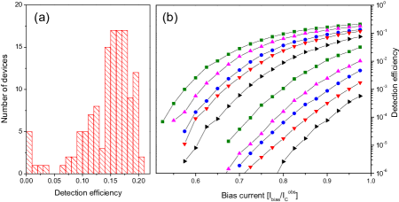
Figure 1 illustrates the detection efficiency (DE) variations observed on a single chip of 132 devices of the same geometry, fabricated in a single run. These devices are the same ones reported in Ref. cavity before the optical cavities were added (maximum DE after the addition of cavities was 57%). In panel (a) we show a histogram of the measured detection efficiencies at (where is the observed critical current of each device), and (b) shows some representative data of the observed DE as a function of . Note that the shape of these curves also varies significantly. As we show below, these data can be explained with the hypothesis, first suggested in Ref. constrict , that some devices have “constrictions:” regions where the (superconducting) cross-sectional area of the wire is reduced by a factor we label . This effectively reduces the observed critical current by that same factor (), and prevents the current density everywhere but near the constriction from ever approaching the critical value (and hence prevents the wire from having a high DE except locally near the constriction).
If all the nanowires were identical in all dimensions save for a pointlike constriction, we would expect that if the data of Fig. 1(b) were plotted vs. absolute current (rather than ) it would all lie on a single, universal curve, with the data for more constricted devices simply not extending to as high currents. This turns out to be approximately true, but variations from device to device across the chip either in film thickness or in the nanowire width obscure this essential feature of the data when it is plotted in this simple way. Instead, we present our results as shown in Fig. 2. In panel (a), the DE data for each of 170 devices with 90 nm wide wires (across two chips fabricated in separate runs) is shown superposed (filled circles indicate K, and crosses K). All of the data for each temperature can be made to lie on a single universal curve by scaling the critical current for each device by an adjustable factor (which is just : ). The very fact that data from this many devices can be so well superposed is already suggestive of a universal shape. However, we can now take the value for each device extracted using this scaling procedure and cross-check it. Based on our previous discussion, if all wires were identical save for constrictions, we would expect , i.e. to be exactly proportional to . Due to the variations across a chip discussed above, this is only partially true. However, we can normalize out these variations using a very simple method: instead of comparing directly to , we instead compare it to the product , where and are the cross-sectional area and room-temperature resistance of each nanowire, and are the critical current density and room-temperature resistivity of NbN, respectively, and is the total wire length. This product depends on the wire geometry only through (which is fixed lithographically and does not vary appreciably between devices) and not on each wire’s individual . Figures 2(b) and (c) show a comparison between the values extracted from the data in Fig. 2(a) and the product. The data lie on a straight line through the origin, indicating that these two independent measures of are mutually self-consistent.
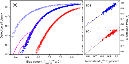
Our data can also be used to infer that the constrictions are essentially pointlike (i.e. very short in length). The open circles in Fig. 2(a) are data for 15 devices with 54 nm wide wires, and clearly show a dramatically different shape (i.e. high DE persists to much lower currents than for the wider wires). The broken lines are estimates, based on the data for 90 nm and 54 nm wide wires, of what one would expect for a device having 90 nm wide wire, except at a single constriction 54 nm wide (corresponding to ) with a length of either 0.5 m (dashed line) or 50 nm (dotted line) long. These curves have a different shape from the data for 90 nm wide wires, because at low currents the DE is dominated by the region of wire near the constriction, while at higher current it becomes dominated by the contribution from the rest of the wire length. This very different shape should be distinguishable if it were present, and should prevent the data from being superposed onto a single curve. The absence of this in our data at any level above the noise indicates that the constricted regions are likely much shorter than 0.5m.
So far, we have in fact only measured constriction in a relative sense; that is, we have no way to tell if our best devices in fact have . To address this, we can exploit the known dependence of the kinetic inductance on bias current. Kinetic inductance arises from energy stored in the effectively ballistic motion of Cooper pairs; as the current density is increased towards the critical value, the density of Cooper pairs is depleted, forcing the remaining pairs to speed up (and therefore store more kinetic energy per unit volume) to maintain the current. Hence, the kinetic inductance increases as orlando . Since the kinetic inductivity locally increases with , the total kinetic inductance of the wire provides a way to determine if the current density is indeed near the critical value over the whole wire or only at one localized place. We measured the inductance of our nanowires using a network analyzer, by observing the phase of a reflected microwave signal as a function of frequency. We then fit this data using a suitable electrical model to extract the inductance value. A bias tee was inserted into the signal path to superpose the desired with the network analyzer output. The phase contributions from the coaxial cable, bias tee, and microwave probe were removed by probing an in situ microwave calibration standard (GGB Industries CS-5). The microwave power used in this measurement corresponds to a peak current amplitude of , and the critical current measured in the presence of the microwaves was within 10% of that measured in their absence (A for typical devices at K).
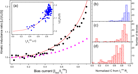
In Fig. 3(a), we show the measured inductance vs. current of two devices; one which has nearly the highest detection efficiency observed on this chip (22% - filled circles), and the other having one of the lowest (0.1% - filled triangles). Also shown is the prediction for from Ginsburg-Landau theory (see, e.g., orlando ), with no free parameters (solid line). The data for the high-DE device show good agreement with this prediction, indicating that this device is indeed unconstricted. However, for the low-DE device the inductance does not increase as much as predicted, which is precisely what we would expect within the constriction hypothesis; the current density is only near critical at one localized place (which constitutes a negligible fraction of the total wire length) whereas everywhere else the current density is lower, producing a smaller increase in inductance. The factor by which must be rescaled for a given device so that the data matches the prediction constitutes an absolute measurement of . One such measurement for a single representative device, from among a large set of nominally identical devices, then allows us to correctly normalize the values obtained using either of the previous methods described above (see Fig. 2) for all other devices in that set.
We can also verify that the observed and product give mutually consistent results. To check this, for each device we measured the inductance ratio , where . Using the obtained from the normalized product, we also obtain for each device. The inset to Fig. 3(a) shows vs. (filled squares), and the data are in reasonable agreement with the Ginsburg-Landau prediction (solid line).
In addition to providing evidence for the constriction hypothesis, the measurement of and provide a powerful diagnostic tool, since they constitute a purely electrical measurement of , which can then be used to predict the detection efficiency, as indicated in Figs. 2(b) and (c). Since optical testing of large numbers of detectors is significantly more difficult and time-consuming than electrical testing, this is potentially an important screening technique. An example of data obtained with this technique is shown in Figs. 3(b), (c), and (d). For three sets of devices, we obtained values from , normalized using a single absolute measurement of for each set via as described above. Panel (b) shows data for the set of devices from Fig. 1(a); panels (c) and (d) show results for a sample of 310 additional devices on a single additional chip, all having 90 nm wide wires on a 200 nm pitch, but with active areas of both (c) 3 3.3 m, and (d) 10 10 m. The devices from (b) and (c), which are nominally identical, exhibit very similar distributions (though some yield fluctuation, which we commonly observe, is evident). Panels (c) and (d), however, clearly show a lower average for the larger-area devices, qualitatively consistent with some fixed area density of constrictions. This implies that at the present state of film growth and nanowire patterning, the yield for high-DE single devices or device arrays covering 10 10 m areas or larger will likely be quite low.
As a final note, we remark on the obvious question of the origin of these constrictions. The most natural explanation would be lithographic patterning errors; for example, a small particle or defect in the resist before exposure could result in a localized narrow section of wire. However, we have performed extensive scanning electron microscopy of devices that were measured to be severely constricted (e.g. ) and no such errors were observable. This suggests that constrictions in our devices result either from thickness variations or material defects, which may have been present in the film before patterning, and may even be due to defects present in the substrate itself before film growth.
In conclusion, we have verified both optically and electrically that the large variations in detection efficiency between nominally identical superconducting nanowire single photon detectors are the result of localized constrictions which limit the device current. Further work is ongoing to pin down the exact source of these constrictions, with the hope of eventually fabricating large arrays of these detectors.
This work is sponsored by the United States Air Force under Air Force Contract #FA8721-05-C-0002. Opinions, interpretations, recommendations and conclusions are those of the authors and are not necessarily endorsed by the United States Government.
References
- (1) G. Gol tsman, O. Okunev, G. Chulkova, A. Lipatov, A. Dzardanov, K. Smirnov, A. Semenov, B. Voronov, C. Williams, and R. Sobolewski, IEEE Trans. Appl. Supercond. 11, pp. 574-577 (2001); A. Engel, A. Semenov, H.-W. Hübers, K. Il’in, and M. Siegel, J. Mod. Opt. 51, pp. 1459-1466 (2004); B. Delaet, J.-C. Villégier, W. Escoffier, J.-L. Thomassin, P. Feautrier, I. Wang, P. Renaud-Goud and J.-P. Poizat, Nucl. Inst. Meth. Phys. Res. A 520, pp. 541-543 (2004).
- (2) K.M. Rosfjord, J.K.W. Yang, E.A. Dauler, A.J. Kerman, V. Anant, B.M. Voronov, G.N. Gol’tsman, and K.K. Berggren, Opt. Express. 14, pp. 527-534 (2006).
- (3) J. Zhang, W. Slysz, A. Verevkin, O. Okunev, G. Chulkova, A. Korneev, A. Lipatov, G. N. Gol’tsman, and R. Sobolewski, IEEE Trans. Appl. Supercond. 13, pp. 180-183 (2003).
- (4) A.J. Kerman, E.A. Dauler, W.E. Keicher, J.K.W. Yang, K.K. Berggren, G.N. Gol’tsman, and B.M. Voronov, Appl. Phys. Lett. 88, p. 111116 (2006).
- (5) E.A. Dauler, B.S. Robinson, A.J. Kerman, J.K.W. Yang, K.M. Rosfjord, V.Anant, B. Voronov, G. Gol’tsman, and K.K. Berggren, IEEE Trans. Appl. Supercond., to be published.
- (6) B.S. Robinson, A.J. Kerman, E.A. Dauler, R.J. Barron, D.O. Caplan, M.L. Stevens, J.J. Carney, S.A. Hamilton, J.K.W. Yang, and K.K. Berggren, Optics Lett. 31, p. 444 (2006).
- (7) R.H. Hadfield, M.J. Stevens, S.S. Gruber, A.J. Miller, R.E. Schwall, R.P. Mirin, and S.W. Nam, Opt. Express 13, pp. 10846-10853 (2005);
- (8) M.J. Stevens, R.H. Hadfield, R.E. Schwall, S.W. Nam, R.P. Mirin, and J.A. Gupta, Appl. Phys. Lett. 89, 031109 (2006).
- (9) M.A. Jaspan, J.L. Habif, R.H. Hadfield, and S.W. Nam, Appl. Phys. Lett. 89, 031112 (2006).
- (10) A. Korneev, A. Lipatov, O. Okunev, G. Chulkova, K. Smirnov, G. Gol tsman, J. Zhang, W. Słysz, A. Verevkin, R. Sobolewski, Microelec. Eng. 69, p. 274 (2003).
- (11) W. Słysz, M. Wȩgrzecki, J. Bar, P. Grabiec, M. G rska, V. Zwiller, C. Latta, P. Bohi, I. Milostnaya, O. Minaeva, A. Antipov, O. Okunev, A. Korneev, K. Smirnov, B. Voronov, N. Kaurova, G. Gol tsman, A. Pearlman, A. Cross, I. Komissarov, A. Verevkin, and R. Sobolewski, Appl. Phys. Lett. 88, p. 261113 (2006).
- (12) E.A. Dauler, B.S. Robinson, A.J. Kerman, V. Anant, R.J. Barron, K.K. Berggren, D.O. Caplan, J.J. Carney, S.A. Hamilton, K.M. Rosfjord, M.L. Stevens, and J.K.W. Yang, Proc. SPIE, to be published.
- (13) J.K.W. Yang, A.J. Kerman, E.A. Dauler, V. Anant, K.M. Rosfjord, K.K. Berggren, IEEE Trans. Appl. Supercond., to be published.
- (14) J.K.W. Yang, E. Dauler, A. Ferri, A. Pearlman, A. Verevkin, G. Gol’tsman, B. Voronov, R. Sobolewski, W.E. Keicher, and K.K. Berggren, IEEE Trans. Appl. Supercond. 15, pp. 626-629 (2005).
- (15) S. Cherednichenko, P.Yagoubov, K. Il’in, G. Gol’tsman, and E. Gershenzon, in Proceedings of the 8th International Symposium On Space Terahertz Technology, Boston, MA, 1997, p. 245.
- (16) J. Zhang, W. Słysz, A. Pearlman, A. Verevkin, R. Sobolewski, O. Okunev, G. Chulkova, and G. N. Gol tsman, Phys. Rev. B 67, p. 132508 (2003).
- (17) T.P. Orlando and K.A. Delin, Foundations of Applied Superconductivity, Addison-Wesley, New York (1991).