The Modern FPGA as Discriminator, TDC and ADC
Abstract
Recent generations of Field Programmable Gate Arrays (FPGAs) have become indispensable tools for complex state machine control and signal processing, and now routinely incorporate CPU cores to allow execution of user software code. At the same time, their exceptional performance permits low-power implementation of functionality previously the exclusive domain of dedicated analog electronics. Specific examples presented here use FPGAs as discriminator, time-to-digital (TDC) and analog-to-digital converter (ADC). All three cases are examples of instrumentation for current or future astroparticle experiments.
I Motivation
Recent generations of Field Programmable Gate Arrays (FPGAs) have become incredibly powerful logic devices. With companion sensors and a data interface, they become valuable data collection nodes for the physical sciences. For certain applications, it has become apparent that these logic devices themselves can serve as the crucial processing elements of instrumentation electronics. Specific applications where this resource can be tapped include, but are not limited to:
-
•
compact form factor (complete system with very small footprint)
-
•
ultra low-power compared with discrete systems of comparable functionality
-
•
input-output (I/O) limited systems
-
•
low Electromagnetic Interference (EMI)
Specific examples presented here use the Xilinx Spartan-3 FPGA, a low-cost and flexible device generously made available through the Xilinx University Program XUP . High performance instrumentation is increasingly a marriage between custom Application Specific Integrated Circuits (ASICs) and high performance FPGAs, capable of processing and transmitting the data collected. In certain applications, the external circuitry simplifies dramatically, and much of the critical functionality can be provided by the FPGA itself.
Three examples are presented here as solutions to power, size and noise constraints of current and planned neutrino detection experiments. While specific to these fields, the techniques are generally applicable to measurement requirements in other disciplines.
II ANITA Discriminator
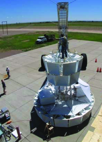
The Antarctic Impulsive Transient Antenna (ANITA) ANITA SNIC experiment is a balloon-borne payload targeted to make the first observation of the flux of ultra-high energy neutrinos, which must exist due to the presence of the high-energy flux of cosmic ray protons. ANITA uses the generation of impulsive radio signals in the Antarctic ice, produced by neutrino interactions at very high energy, as the detection method. A photograph of the ANITA payload preparing for its engineering flight in New Mexico is seen in Fig. 1.
As a long-duration balloon-borne payload over the Antarctic continent, power is a severe constraint on the instrumentation. Particularly for triggering and sampling many dozens of antennas over the full bandwidth of 0.2-1.2 GHz, with greater than Nyquist sampling. The strategy adopted for ANITA is to split the signal as shown in Fig. 2 and use the trigger information to decide when the analog samples SPIE ; LAB should be held and digitized. This scheme can reduce the power required by two orders of magnitude or more.

II.1 Triggering
In order to distinguish background thermal noise from transient radio-frequency signatures of neutrino interactions, the primary trigger consists of 256 channels of high-speed discriminator. A discriminator is a combination of a fast comparator and a 1-shot circuit to give a signal passing threshold a fixed width output for the purposes of forming a well-defined signal coincidence.
In order to meet the physics requirements, thresholds for the trigger must be pushed as far down into the thermal noise as can be sustained. Studies indicate SMEX that this corresponds to single filter-band trigger rates of 1-2MHz. Operation at such a high rate near threshold requires a comparator of exceedingly high gain-bandwidth (GBW) product. In addition, such comparators are likely to produce significant amounts of EMI due to fast switching output signals.
Within the FPGA considered, it turns out that with proper threshold setting, the Low-Voltage Differential Signaling (LVDS) LVDS comparator inputs provide exceptional GBW performance. Internal logic can be used to form an adjustable width output 1-shot circuit, immune from “runt” (very narrow temporal pulse) generation, which is a common problem in this type of discriminator logic. This circuitry is illustrated in Fig. 3.
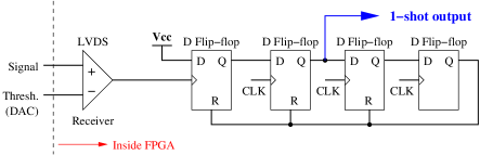
Using a 250MHz CLK signal, generated from the Digital Clock Manager (DCM) as derived from a 33MHz (PCI clock) reference, the discriminator output can be quantized in 4ns steps.
Avoiding full signal swings external to the FPGA helps in two significant ways: it reduces the power required by providing the input directly to the FPGA, and just as importantly, it reduces the EMI and board-level noise induced by large, fast external switching signals.
II.2 Implementation
The printed circuit board on which this discriminator is placed is denoted the Sampling Unit for Radio Frequency (SURF) board and a photo of the production board stack may be seen in Fig. 4. The SURF form factor is 6U Eurocard and is designed to work in a conduction-cooled compact-PCI crate.
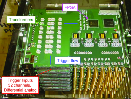
Conduction-cooling operation requires heat sinking (not shown) and places emphasis on reducing component heat load.
Four filter-banded trigger signals for both polarizations of four quad-ridge horn antennas are brought into the high density input connector indicated. These 32 differential analog signals are converted to 50 single-ended signals, where the other side of the transformer is held at a reference potential which optimizes the signal range to that of the LVDS receiver inputs. Buried microstrip lines are terminated in 50 termination resistors very close to the FPGA. The trigger thresholds are set by applying a voltage to the complementary input of the LVDS receiver, as seen in Fig. 3. As this input is high-impedance, threshold setting may be done with an array of compact, low-power, multi-channel output DACs. Performance of this circuit is presented in detail in the next subsection.
An early prototype version of this board made use of eight 4-channel high-speed comparators, which required additional space, power, and produced significant noise. With proper shielding, careful layout, and working with small amplitude swings, the board level noise was reduced drastically and appears largely dominated by ambient crate noise.
II.3 Performance
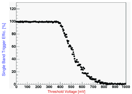
Performance of this discriminator was evaluated in a number of ways. As a first step, a simple scan of count rate versus threshold for amplified thermal noise, approximating the expected amplitude in flight, was performed as shown in Fig. 5
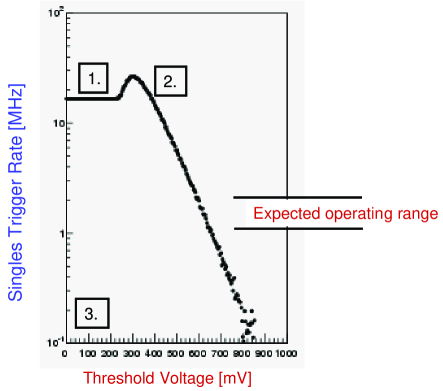
The curve follows expectations, considering three key features of the 12-ns output width 1-shot logic (adjustable in 4ns clock steps) and its “stuck on” detect circuit. These features are enumerated in the figure and explained in detail below.
-
1.
Saturation at 16MHz is the result of a “stuck on” detect circuit, which is used to resolve the potential ambiguity in absolute trigger rate. That is, a measured rate could be due to the signal just poking above threshold at a rate of 1MHz or only dropping below threshold at a rate of 1MHz. This circuit detects the latter condition and enforces a minimum rate of 16MHz when the threshold is too low.
-
2.
The curve deviates from linear on this plot as the 12ns 1-shot deadtime starts to become important. At 8.3MHz (120ns average period), this becomes a 10% effect and eventually leads to the curve rolling over, as can be seen.
-
3.
Threshold voltage shown is on a relative scale with respect to a voltage offset; only the relative voltage is important.
Next a signal is embedded in the noise and the trigger efficiency is studied as a function of threshold. This scan is seen in Fig. 6 for a signal of about the minimum assumed in Monte Carlo simulation of the ANITA sensitivity. A trigger is determined if a discriminator signal is coincident within 20ns of a reference strobe from the pulse generator used.
Finally trigger efficiency is studied as a function of the threshold, for the embedded signal with a Signal-to-Noise Ratio (SNR) of about 4.1 before filter banding. As can be seen in Fig. 7, the efficiency is tuned as a function of the tolerable singles rate in each channel.
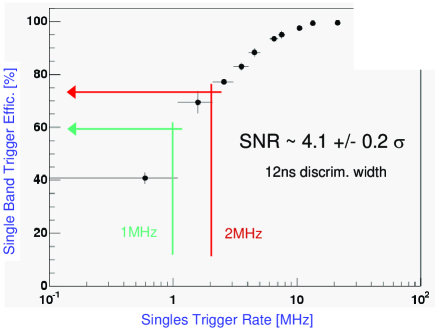
The limit on this rate is dictated by the overall accidental trigger rate downstream, which we expect to be in the range indicated. Since the antenna trigger efficiency requires only a 3-of-8 coincidence, the overall efficiency improves as can be seen in Fig. 8.
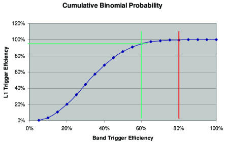
As seen in the figure, if an efficiency of about 80% can be maintained in each band, the overall Antenna-level trigger (“Level 1” (L1)) efficiency is essentially unity. Even a degradation to 60% single band efficiency means an L1 efficiency of roughly 95%.
In order to check the performance of the 1-shot circuit and coincidence logic, a scan of L1 Rate was performed as a function of single band rates for only thermal noise input (no signal). The resultant plot is seen in Fig. 9.
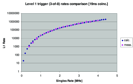
Overlaid is the expected curve for the cumulative binomial probability of purely random trigger band signals. The two curves are in good agreement for an effective coincidence window of 19ns, indicating a 5ns coincidence overlap requirement.
III HanoHano TDC and QDC
Detecting the much lower energy neutrinos due to nuclear fission or fusion requires a detector of ultra-pure material. The KamLAND detector KamLAND has been very successful in measuring solar neutrinos, as well as those from nearby power plants in Japan. However, the naturally occurring radioactivity in the surrounding mountains limit the sensitivity to possible neutrinos from decays deep inside the earth. To search for these and possible hidden nuclear reactors, operation of such a detector deep in the ocean is of interest. A prototype of such a detector, designated HanoHano HanoHano , may be seen in Fig. 10.
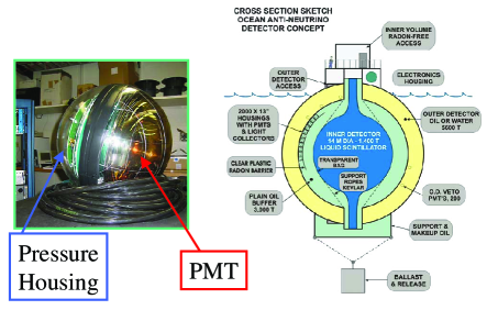
The detector consists of a large volume of ultra-pure liquid scintillator observed by a large array of Photo-Multiplier Tubes (PMTs). Deployment of such an extensive array far at sea is best done without the requirements of a shore cable. Therefore powering from a battery system is very attractive if it can be made feasible. Having a single FPGA serve as Time-to-Digital Converter (TDC), charge(Q)-to-Digital Converter (QDC) and data collection node, for a large number of PMTs, represents a great power savings.
Signal flow for the encoding of the PMT times in this readout can be seen in Fig. 11. Again the LVDS receiver of the FPGA is used as the comparator input. The output of this comparator is used to latch a time of the leading edge to measure time and the trailing edge to measure the total charge Q, which is proportional to the time-over-threshold.
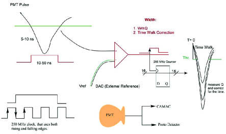
Using both edges of a 250MHz clock, the expected ideal time resolution should be
| (1) |
where is the 2ns period when using both clock edges. In this case, a resolution of about 0.6 ns is theoretically possible and is explored below.
III.1 Readout Implementation
A prototype board for doing this readout can be seen in Fig. 12
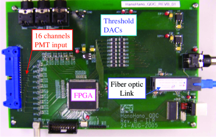
A bundle of 16 PMT signals are brought onto the board via ribbon cable at left and into the FPGA. Continuous logging of the T and Q values for each PMT hit is performed inside the FPGA and dumped into an on-chip FIFO. Data from this FIFO is collected over a fiber optic link (at the right) to the central data acquisition computer.
III.2 Test Results
The results from a simple Gray-code counter implementation of the hit time recording may be seen in Fig. 13. The sigma of the distribution is about 1ns, but there are non-Gaussian tails. In this case the RMS resolution of about 1.3ns is more representative.
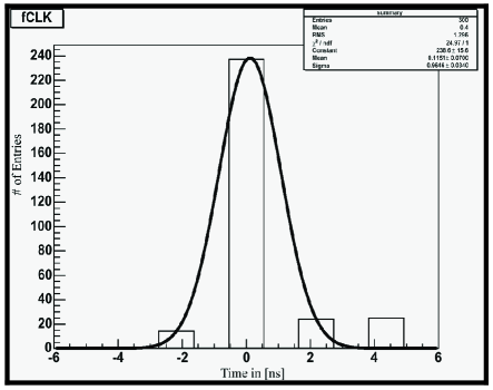
While this is a factor of two worse than theoretical, it should be pointed out that since the HanoHano PMTs are largely recording single photons, and these large PMTs being employed have a Transit-Time-Spread (TTS) of 3ns, the expected resolution will only degrade to
| (2) |
or by about 10%. Nevertheless, since high clock speeds and more clever algorithms are possible, better timing will continue to be pursed.
IV SalSA ADC
Should the ANITA experiment confirm the expected flux of GZK neutrinos, a next generation of terrestrial neutrino telescope will exploit this source for both astronomy and particle physics. An example of such a detector is the proposed Salt-dome Shower Array (SalSA) SalSA . A schematic view of such a detector may be seen in Fig. 14, where an array of drill holes into the salt (or ice) are instrumented with strings of antennas.
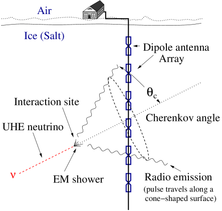
As indicated in the figure, salt has the advantage of being 2.4 times as dense as ice and of equally high radio transmission. An earlier study of low-cost readout was performed using short waveform sample buffers GEISER . Further studies have indicated that to optimize neutrino flavor identification, improvements to the current generation of low-power, compact Radio-Frequency sampling ASICs SPIE ; LAB will involve a readout capable of much longer waveform samples.
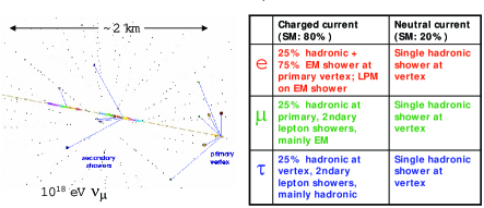
This may be seen in Fig. 15. Particle identification is possible by the flavor-specific pattern of subthreshold emissions (secondary showers) along the lepton track. However, to do so requires the ability to store record lengths of order of the transit time across the array in order to capture subthreshold signals.
A proposal BLAB1 was written to MOSIS MOSIS to fund the fabrication of a test ASIC in a 0.25m CMOS process. This device has 64k deep sampling, which provides for up to 32s of storage at 2GSa/s. In order to accommodate so many devices on a relatively small die, the conversion of the storage samples using a Wilkinson-type ADC is performed by the companion FPGA. This scheme is illustrated in Fig. 16.
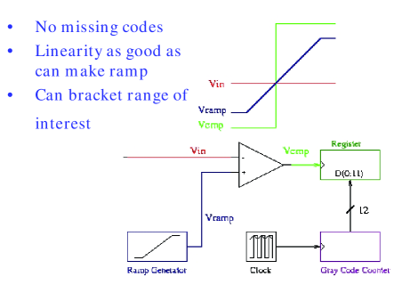
This scheme is quite general and with the use of an array of external sample/hold circuits, or for rather slow speed signals, direct conversion of analog signals with the FPGA may be performed. Experience has shown that the performance of this type of encoding is limited by the quality of the clock source and the linearity of the ramp. Fortunately the on-chip PLL provides for quite stable clock sources and because the LVDS inputs are high impedance, a very simple and yet high-quality ramp generator can be made with a current source, a capacitor and a reset transistor.
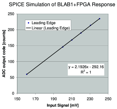
Performance simulations have been done in SPICE and may be seen in Fig. 17. The ASIC is currently in fabrication.
One advantage of performing the time encoding in programmable logic is that the resolution can be tailored to the application. A trade-off can be made between speed and resolution in a highly flexible way.
V Future Prospects
Future generations of FPGA will continue to improve in speed and operate at reduced voltage levels. For applications requiring good timing, this will certainly be an improvement. Current generations of Xilinx already provide a stable 10GHz clock reference for the “Rocket I/O” interface. Having access to this clock would permit a theoretical direct timing resolution of:
| (3) |
However, at lower operating voltages, the limited dynamic range will also prove a challenge. Already these low rail voltages are an issue in many mixed-signal applications.
VI Acknowledgements
This work was enabled by the generous support of the ANITA collaboration under the NASA Research Opportunities in Space Science (ROSS) program, the HanoHano collaboration under the Center for Excellence in Research in Ocean Science (CEROS) program, the MOSIS Educational Program and the Xilinx University Program.
References
- (1) Xilinx University Program provides a donation program (http://www.xilinx.com/univ) to higher education that has benefitted all of the research projects described.
- (2) P. Miocinovic et al. [ANITA Collaboration], “Tuning into UHE neutrinos in Antarctica: The ANITA experiment”, eConf C041213, 2516 (2004); hep-ex/0503304.
- (3) G. Varner et al. [ANITA Collaboration], “Detection of Ultra High Energy Neutrinos via Coherent Radio Emission”, to appear in the Proceedings of the Stanford-Novosibirsk Instrumentation Conference 2006, SLAC, April 2006.
- (4) G. Varner et al., “Monolithic Multi-channel GSa/s Transient Waveform Recorder for Measuring Radio Emissions from High Energy Particle Cascades”, Proc. SPIE Int. Soc. Opt. Eng. 4858-31, 2003.
- (5) G. Varner, J. Cao, M. Wilcox and P. Gorham, “Large Analog Bandwidth Recorder and Digitizer with Ordered Readout (LABRADOR) ASIC.”, manuscript in preparation for submission to Nucl. Instr. Meth. A, available online as physics/0509023.
-
(6)
ANITA Phase A proposal for the NASA
Small Explorer (SMEX) program, available online:
www.phys.hawaii.edu/
anita/web/project/proposal/anitaprop.pdf - (7) Low-voltage differential signaling (LVDS) uses high-speed analog circuit techniques to provide multi-gigabit data transfers on copper interconnects. It is defined under the Electronic Industries Alliance (EIA)-644-1995 standard.
- (8) J.S. Ricol et al. (KamLAND Collaboration), “KamLAND status and results”, EPS International Europhysics Conference on High Energy Physics (HEP-EPS 2005), Lisbon, Portugal July 2005. PoS HEP2005:174, 2006.
- (9) S. Dye et al. (HanoHano Collaboration), “HanoHano: Detector Size and Sensitivity”, to appear in the proceedings of the Neutrino Sciences 2005 - Geoneutrino Conference, Honolulu, Hawaii, Dec. 2005. Online link: www.phys.hawaii.edu/sdye/hnsc.html
- (10) P. Gorham et al., “Accelerator Measurements of the Askaryan Effect in Rock Salt: A roadmap toward teraton underground neutrino detectors.”, Phys. Rev. D 72 023002 (2005).
- (11) G. Varner et al., “A Giga-bit Ethernet Instrument for SalSA Experiment Readout”, Nucl. Instr. Meth. A 554 (2005) 437-443.
- (12) G. Varner, “Proposal to Fabricate: First Buffered LABRADOR (BLAB1) ASIC for High Speed Applications”. Proposal awarded March, 2006.
- (13) The MOSIS multi-project wafer service is operated via the University of Southern California, http://www.mosis.org