Effect of magnetization inhomogeneity on magnetic microtraps for atoms
Abstract
We report on the origin of fragmentation of ultracold atoms observed on a magnetic film atom chip. Radio frequency spectroscopy and optical imaging of the trapped atoms is used to characterize small spatial variations of the magnetic field near the film surface. Direct observations indicate the fragmentation is due to a corrugation of the magnetic potential caused by long range inhomogeneity in the film magnetization. A model which takes into account two-dimensional variations of the film magnetization is consistent with the observations.
pacs:
03.75.Be, 07.55.Ge, 34.50.Dy, 39.25.+kAn atom chip is designed to manipulate magnetically trapped ultracold atoms near a surface using an arrangement of microfabricated wires or patterned magnetic materials Folman et al. (2002). Since the realization of Bose-Einstein condensates (BECs) on atom chips Hänsel et al. (2001); Ott et al. (2001), pioneering experiments have studied single-mode propagation along waveguides Leanhardt et al. (2002), transport and adiabatic splitting of a BEC Hommelhoff et al. (2005) and recently on-chip atom interferometry Shin et al. (2005); Schumm et al. (2005). Permanent magnets are particularly attractive for atom chips as they can provide complex magnetic potentials Sidorov et al. (2002) while suppressing current noise that causes heating and limits the lifetime of trapped atoms near a surface Sinclair et al. (2005a). To date, permanent magnet atom chips have been developed with a view to study one-dimensional quantum gases Vengalattore et al. (2004); Llorente-Garcia et al. (2005); Boyd et al. (2006), decoherence of BEC near surfaces Sinclair et al. (2005a); Hall et al. (2006a), hybrid magnetic and optical trapping configurations Jaakkola et al. (2005), and self biased fully permanent magnetic potentials Barb et al. (2005). It has been found, however, that in addition to current noise, atom chips have other limitations, as undesired spatial magnetic field variations associated with the current-carrying wires or magnetic materials act to fragment the trapped atoms.
In previous work, fragmentation of atoms trapped near current-carrying wires was traced to roughness of the wire edges that causes tiny current deviations Wang et al. (2004); Estève et al. (2004). This introduces a spatially varying magnetic field component parallel to the wire which corrugates the bottom of the trap potential. While more advanced microfabrication techniques have been used to produce wires with extremely straight edges, thereby minimizing fragmentation Krüger et al. (2004); Pietra et al. (2005), the first experiments with permanent magnet atom chips have now also indicated the presence of significant fragmentation Sinclair et al. (2005b); Hall et al. (2005); Boyd et al. (2006). This has motivated further work towards understanding the mechanisms that cause fragmentation near magnetic materials.
In this paper we report on the origin of fragmentation near the surface of a permanent magnetic film atom chip. To characterize the magnetic field near the film surface we have developed a technique which combines precision radio frequency (rf) spectroscopy of trapped atoms with high spatial resolution optical imaging. This allows sensitive and intrinsically calibrated measurements of the magnetic field landscape to be made over a large area. We find the fragmentation originates from long range inhomogeneity in the film magnetization and has characteristics that differ from those observed for current-carrying wire atom chips. To account for the observations we have developed a model for the spatial decay of random magnetic fields from the surface due to inhomogeneity in the film magnetization.
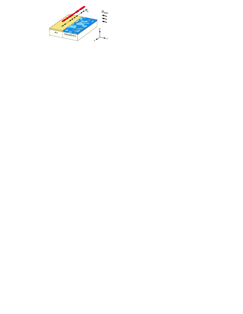
A schematic diagram of a basic magnetic film atom chip is shown in Fig. 1. Our atom chip uses a Tb6Gd10Fe80Co4 film which exhibits strong perpendicular anisotropy Hall et al. (2006a). The edge of the µm thick glass-slide substrate is polished to optical quality prior to film deposition. Scanning profilometer measurements on similarly prepared substrates indicate that the residual edge roughness is less than 50 nm and the top surface is extremely smooth. The substrate is sputter-coated with a multilayer magnetic film ( nm TbGdFeCo and nm Cr) and a gold overlayer (100 nm), and the film topology accurately follows that of the polished substrate. The deposited film has been analyzed using a SQUID magnetometer and a magnetic force microscope (MFM) and has shown excellent magnetic properties Wang et al. (2005). The film is magnetized perpendicular to the surface by a magnetic field of 1 T and afterwards is magnetically homogeneous within the sensitivity of the MFM. A second glass slide, coated with a non-magnetic gold film, completes the reflective atom chip surface (Fig. 1). Both substrates are then epoxied to a µm thick silver foil current-carrying structure which is used for loading ultracold atoms into the permanent magnet microtrap, to provide weak longitudinal confinement, and as an in-built radio frequency antenna.
At the edge of the perpendicularly magnetized film a field is produced that is analogous to that of a thin current-carrying wire aligned with the film edge (A) Sidorov et al. (2002); Hall et al. (2006a). A magnetic microtrap is formed by the field from the film, a uniform magnetic field , and two current-carrying end-wires. In the experiment 87Rb atoms are collected in a mirror magneto-optical trap located 5 mm from the surface. These atoms are optically pumped to the hyperfine state and subsequently transferred to a magnetic trap formed by a Z-shaped current-carrying wire and . A preliminary rf evaporative cooling stage is used to reduce the cloud temperature below 5 µK. The remaining atoms are then transferred to the magnetic film microtrap by adiabatically reducing the current through the Z-shaped wire to zero. The final values of vary from 0.2 mT to 0.8 mT, so the transverse trap frequency varies between Hz and Hz while the trap position ranges from 200 µm to 50 µm from the surface. The end-wires are operated at 0.5 A such that the trap depth is 100 µK and the elongated cloud of atoms extends 5 mm along the edge of the atom chip to allow measurement of the magnetic potential.
The narrow energy distribution of ultracold atoms is an inherent advantage when used as a probe of weak potentials. In particular, the equilibrium distribution of trapped atoms has been used to image magnetic fields near test wires with high sensitivity and high spatial resolution Wildermuth et al. (2005); Günther et al. (2005). In parallel, rf spectroscopy has been used as a precise and powerful method for investigating the properties of cold atom clouds Martin et al. (1988); Helmerson et al. (1992); Bloch et al. (1999); Gupta et al. (2003); Chin et al. (2004). In this paper we use rf spectroscopy of ultracold atoms to accurately profile small magnetic field variations near the magnetic film surface.
A spatially uniform rf field of frequency is applied perpendicular to the trap axis to resonantly outcouple atoms to untrapped magnetic states at positions where . The rf field is swept using a single frequency ramp (0.2 MHz/s) from 2 MHz to a final cut-off frequency ranging between 1.4 MHz and 0.5 MHz. The Rabi frequency of the rf transition is kHz, high enough to ensure that atoms with total energy greater than are removed from the trap with high probability and that regions of the potential where thereafter remain unpopulated. During the early stages of the rf sweep the cloud undergoes some evaporative cooling as the in-trap collision rate is high enough to allow rethermalization. At the end of the sweep the resonant frequency approaches that corresponding to the trap bottom and the cloud becomes significantly truncated by the rf field.
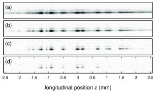
Immediately after the sweep, is switched off to accelerate the atoms away from the film surface in the remaining permanent magnetic field gradient. The longitudinal density distribution is unperturbed during the 1 ms expansion time and is an accurate representation of the in-trap distribution. A resonant absorption image is then recorded by a CCD with a spatial resolution of µm. A series of absorption images for different values of is shown in Fig. 2. Noticeable fragmentation is observed when is reduced below 1.3 MHz (Fig. 2a). For MHz the density distribution becomes truncated by the rf field and regions of the atomic density decrease to zero (Fig. 2b). Reducing further results in well separated clumps of atoms which are found only in the lowest potential wells (Fig. 2c, d).
For a quantitative analysis we assume that the full trapping potential can be expressed in terms of the transverse confinement and the corrugated longitudinal potential where is the value of the uniform offset field Estève et al. (2004). The atomic distribution in the trap immediately after the rf sweep is described by a truncated Boltzmann distribution Helmerson et al. (1992); Luiten et al. (1996). To extract , the integrated atomic density as a function of can be fit for each position to the truncated thermal distribution function,
| (1) |
where is the integrated atom density before truncation and the spatially dependent truncation parameter is
| (2) |
where is a fit parameter, which characterizes the non-equilibrium distribution during truncation. We find however that this model does not satisfactorily reproduce the density distribution in regions of the potential where the atomic density becomes large; specifically at the bottom of each potential well for lower values of . To minimise this effect we section the full data set into 80 m spatial regions and fit Eq. (1) using a two-dimensional minimisation algorithm as opposed to fitting for each value of independently. This effectively constrains the fitted truncation temperature to vary smoothly over a range corresponding roughly to the extent of a potential well. After reconstructing the magnetic field profile the effect of the end-wires is subtracted. The statistical uncertainty in the measurement is approximately 0.1 µT, which is mainly attributed to fluctuations of external magnetic fields. With appropriate magnetic shielding the expected sensitivity of the technique is limited by the power broadened rf linewidth required to effectively outcouple atoms.
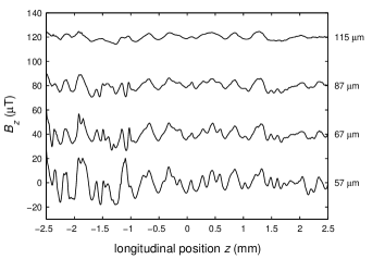
Complete magnetic field profiles are given for several distances from the film in Fig. 3. Firstly, the amplitude and structure of the corrugated potential are constant from day to day; however the amplitude increases as the trap is positioned closer to the surface, with an approximate power law dependence given by , where . For µm the potential has a characteristic period of about 390 µm, significantly longer than that commonly observed near electroplated wires Fortágh et al. (2002); Estève et al. (2004). Closer to the film, additional corrugations appear with a characteristic period of about 170 µm. These -dependent characteristics of the potential have allowed time-dependent manipulation of BECs at particularly interesting regions of the disordered potential Hall et al. (2006b).
The figure of merit for corrugation observed above the TbGdFeCo film is which compares poorly with the current generation of lithographically fabricated wire atom chips Krüger et al. (2004), highlighting the need for further work to improve magnetic materials used in these applications.
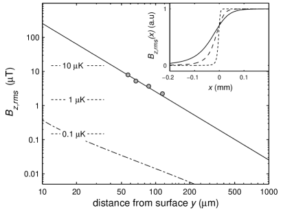
We have found that the amplitude of the corrugated potential is not consistent with magnetostatic calculations based on fluctuations of the film edge (Fig. 4), suggesting that the cause of fragmentation may be spatial variations of the magnetization within the body of the film. To investigate this, a second bias field is applied in the direction to bring the trap closer to the surface while keeping a constant distance from the edge of the magnetic film. A cloud of atoms positioned 50 µm from the surface of the magnetic film and 100 µm from the edge is significantly fragmented, while a cloud positioned 50 µm from the non-magnetic gold film does not exhibit atomic density variations. This observation confirms that the magnetic field variations originate from the magnetic material itself and not from imperfections along the edge of the film.
Our model describes the effect of two-dimensional spatial variations in the perpendicular magnetization of the film. Inhomogeneity leads to the appearance of a random magnetic field above the surface, of which we are most interested in the magnetic field component that corrugates the bottom of the trapping potential. Using a standard approach incorporating the two-dimensional Fourier transform of the random magnetization and the magnetic scalar potential we obtain an expression for the component of the corrugated magnetic field. In the case of a magnetic film occupying a half-plane with the edge at (Fig. 1) and arbitrary magnetization noise we have, for heights greater than the film thickness,
| (3) |
where is the film thickness and is the modified Bessel function of the second kind. In general this expression can be used to describe any planar pattern of elements that can be represented as a linear combination of step functions.
In the case of white noise fluctuations in the magnetization, , the rms value of the magnetic field roughness can be evaluated analytically. We perform ensemble averaging and find
| (4) |
where , is the rms magnetization inhomogeneity and is the characteristic feature size of the domain structure. For the model predicts that the corrugated magnetic field component decays with a dependence, consistent with our experimental result. This behavior can also be compared with the more rapid decay expected for white noise fluctuations of the edge of current-carrying wires Wang et al. (2004); Estève et al. (2004). Film edge fluctuations are expected to produce corrugations three orders of magnitude smaller than that observed in the experiments (Fig. 4). The model also predicts the fast decay of the corrugated magnetic field away from the film edge for (Fig. 4-inset).
In Fig. 4 the experimental results are compared with the model with relevant energy scales indicated by dotted lines. The characteristic feature size and distribution function of the domain structure has been inferred from MFM measurements of a demagnetized TbGdFeCo film and is found to have close to white noise characteristics with µm. The best fit of Eq. (4) to the data is found for 0.3 where is the saturation magnetization of the film. If the inhomogeneity is assumed to originate from reversal of a small number of magnetic domains () then we conclude that the mean magnetization of the film is greater than .
The TbGdFeCo magnetic film was originally chosen for its desirable magnetic properties including a large coercivity ( T) and a high Curie temperature (300∘C) Wang et al. (2005). We attribute the observed inhomogeneity to deterioration of the magnetic film experienced during the vacuum bake-out (140 ∘C over 4 days) despite the relatively high Curie temperature of our film. This conclusion is consistent with reports of reduced perpendicular anisotropy found for similar films after annealing at temperatures above 100∘C Luborsky (1985); Wang and Leng (1990) and with our own measurements on similar films.
In conclusion, trapped ultracold atoms are very sensitive to small magnetic field variations found near the surface of the permanent magnetic film. These variations corrugate the longitudinal trapping potential and result in fragmentation of atomic density. We have developed the technique of spatially resolved rf spectroscopy as a powerful method for accurately mapping small magnetic field variations near the surface of the magnetic film. A simple model accounts for spatial inhomogeneity of the film magnetization and agrees well with the observations. The development of new permanent magnet atom chips will require additional research aimed at further optimizing the quality of magnetic films.
Acknowledgements.
We would like to thank J. Wang for the deposition of the magnetic film. T. Roach acknowledges the Donors of the American Chemical Society Petroleum Research Fund for support during this research. This project is supported by the ARC Centre of Excellence for Quantum-Atom Optics and a Swinburne University Strategic Initiative grant.References
- Folman et al. (2002) R. Folman, P. Krüger, J. Schmiedmayer, J. Denschlag, and C. Henkel, Adv. At. Mol. Opt. Phys. 48, 263 (2002).
- Hänsel et al. (2001) W. Hänsel, P. Hommelhoff, T. W. Hänsch, and J. Reichel, Nature (London) 413, 498 (2001).
- Ott et al. (2001) H. Ott, J. Fortágh, G. Schlotterbeck, A. Grossmann, and C. Zimmermann, Phys. Rev. Lett. 87, 230401 (2001).
- Leanhardt et al. (2002) A. E. Leanhardt, A. P. Chikkatur, D. Kielpinski, Y. Shin, T. L. Gustavson, W. Ketterle, and D. E. Pritchard, Phys. Rev. Lett. 89, 040401 (2002).
- Hommelhoff et al. (2005) P. Hommelhoff, W. Hänsel, T. Steinmetz, T. W. Hänsch, and J. Reichel, New J. Phys. 7, 3 (2005).
- Shin et al. (2005) Y. Shin, C. Sanner, G. B. Jo, T. A. Pasquini, M. Saba, W. Ketterle, D. E. Pritchard, M. Vengalattore, and M. Prentiss, Phys. Rev. A 72, 021604(R) (2005).
- Schumm et al. (2005) T. Schumm, S. Hofferberth, L. M. Andersson, S. Wildermuth, S. Groth, I. Bar-Joseph, J. Schmiedmayer, and P. Krüger, Nature (London) 1, 57 (2005).
- Sidorov et al. (2002) A. I. Sidorov, R. J. McLean, F. Scharnberg, D. S. Gough, T. J. Davis, B. A. Sexton, G. I. Opat, and P. Hannaford, Acta Phys. Pol. B 33, 2137 (2002).
- Sinclair et al. (2005a) C. D. J. Sinclair, E. A. Curtis, I. L. Garcia, J. A. Retter, B. V. Hall, S. Eriksson, B. E. Sauer, and E. A. Hinds, Phys. Rev. A 72, 031603(R) (2005a).
- Vengalattore et al. (2004) M. Vengalattore, R. S. Conroy, W. Rooijakkers, and M. Prentiss, J. Appl. Phys. 95, 4404 (2004).
- Llorente-Garcia et al. (2005) I. Llorente-Garcia, C. D. J. Sinclair, E. A. Curtis, S. Eriksson, B. E. Sauer, and E. A. Hinds, J. Phys.: Conf. Ser. 19, 70 (2005).
- Boyd et al. (2006) M. Boyd, E. W. Streed, P. Medley, G. K. Campbell, J. Mun, W. Ketterle, and D. E. Pritchard, cond-mat/0608370 (2006).
- Hall et al. (2006a) B. V. Hall, S. Whitlock, F. Scharnberg, P. Hannaford, and A. Sidorov, J. Phys. B: At. Mol. Opt. Phys. 39, 27 (2006a).
- Jaakkola et al. (2005) A. Jaakkola, A. Shevchenko, K. Lindfors, M. Hautakorpi, E. Il’yashenko, T. H. Johansen, and M. Kaivola, Eur. Phys. J. D 35, 81 (2005).
- Barb et al. (2005) I. Barb, R. Gerritsma, Y. T. Xing, J. B. Goedkoop, and R. J. C. Spreeuw, Eur. Phys. J. D 35, 75 (2005).
- Wang et al. (2004) D. W. Wang, M. D. Lukin, and E. Demler, Phys. Rev. Lett. 92, 076802 (2004).
- Estève et al. (2004) J. Estève, C. Aussibal, T. Schumm, C. Figl, D. Mailly, I. Bouchoule, C. I. Westbrook, and A. Aspect, Phys. Rev. A 70, 043629 (2004).
- Krüger et al. (2004) P. Krüger, L. M. Andersson, S. Wildermuth, S. Hofferberth, E. Haller, S. Aigner, S. Groth, I. Bar-Joseph, and J. Schmiedmayer, cond-mat/0504686 (2004).
- Pietra et al. (2005) L. D. Pietra, S. Aigner, C. vom Hagen, H. J. Lezec, and J. Schmiedmayer, J. Phys.: Conf. Ser. 19, 30 (2005).
- Sinclair et al. (2005b) C. D. J. Sinclair, J. A. Retter, E. A. Curtis, B. V. Hall, I. Llorente-Garcia, S. Eriksson, B. E. Sauer, and E. A. Hinds, Eur. Phys. J. D 35, 105 (2005b).
- Hall et al. (2005) B. V. Hall, S. Whitlock, F. Scharnberg, P. Hannaford, and A. Sidorov, in Laser Spectroscopy XVII, edited by E. A. Hinds, A. Ferguson, and E. Riis (World Scientific, Singapore, 2005).
- Wang et al. (2005) J. Y. Wang, S. Whitlock, F. Scharnberg, D. Gough, A. I. Sidorov, R. J. McLean, and P. Hannaford, J. Phys. D: Appl. Phys. 38, 4015 (2005).
- Wildermuth et al. (2005) S. Wildermuth, S. Hofferberth, I. Lesanovsky, E. Haller, L. M. Andersson, S. Groth, I. Bar-Joseph, P. Krüger, and J. Schmiedmayer, Nature (London) 435, 440 (2005).
- Günther et al. (2005) A. Günther, M. Kemmler, S. Kraft, C. J. Vale, C. Zimmermann, and J. Fortágh, Phys. Rev. A 71, 063619 (2005).
- Martin et al. (1988) A. G. Martin, K. Helmerson, V. S. Bagnato, G. P. Lafyatis, and D. E. Pritchard, Phys. Rev. Lett. 61, 2431 (1988).
- Helmerson et al. (1992) K. Helmerson, A. G. Martin, and D. E. Pritchard, J. Opt. Soc. Am. B 9, 483 (1992).
- Bloch et al. (1999) I. Bloch, T. W. Hänsch, and T. Esslinger, Phys. Rev. Lett. 82, 3008 (1999).
- Gupta et al. (2003) S. Gupta, Z. Hadzibabic, M. W. Zwierlein, C. A. Stan, K. Dieckmann, C. H. Schunck, E. G. M. van Kempen, B. J. Verhaar, and W. Ketterle, Science 300, 1723 (2003).
- Chin et al. (2004) C. Chin, M. Bartenstein, A. Altmeyer, S. Riedl, S. Jochim, J. H. Denschlag, and R. Grimm, Science 305, 1128 (2004).
- Luiten et al. (1996) O. J. Luiten, M. W. Reynolds, and J. T. M. Walraven, Phys. Rev. A 53, 381 (1996).
- Fortágh et al. (2002) J. Fortágh, H. Ott, S. Kraft, A. Günther, and C. Zimmermann, Phys. Rev. A 66, 041604(R) (2002).
- Hall et al. (2006b) B. V. Hall, S. Whitlock, R. Anderson, P. Hannaford, and A. Sidorov, cond-mat/0609014 (2006b).
- Luborsky (1985) F. E. Luborsky, J. Appl. Phys. 57, 3592 (1985).
- Wang and Leng (1990) Y. J. Wang and Q. W. Leng, Phys. Rev. B 41, 651 (1990).