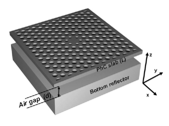
Vertical beaming of wavelength-scale photonic crystal resonators
Abstract
We report that of the photons generated inside a photonic crystal slab resonator can be funneled within a small divergence angle of . The far-field radiation properties of a photonic crystal slab resonant mode are modified by tuning the cavity geometry and by placing a reflector below the cavity. The former method directly shapes the near-field distribution so as to achieve directional and linearly-polarized far-field patterns. The latter modification takes advantage of the interference effect between the original waves and the reflected waves to enhance the energy-directionality. We find that, regardless of the slab thickness, the optimum distance between the slab and the reflector closely equals one wavelength of the resonance under consideration. We have also discussed an efficient far-field simulation algorithm based on the finite-difference time-domain method and the near- to far-field transformation.
pacs:
42.70.Qs, 41.20.Jb, 42.60.DaI Introduction
Multitudes of optical resonant modes can be created by introducing a structural defect into a perfect photonic crystal (PhC) having photonic band gap (PBG). Many researchers have been interested in designing novel nanocavities based on the PhC in the hope of controlling the flow of light in unprecedented ways.Joannopoulos et al. (1997) Especially two-dimensional (2-D) PhC slab structures have been widely studied by utilizing well-established standard fabrication processes.Johnson et al. (1999) In the horizontal directions of such 2-D PhC slab structures, photons can be spatially localized by 2-D photonic bandgap effects. Additionally in the vertical direction, photons are confined rather efficiently through total internal reflection.Johnson et al. (1999); Kim et al. (2004) Air-hole triangular lattices are widely adapted as a basic platform of the 2-D PhC because of their large photonic bandgap.Johnson et al. (1999)
After the first demonstration of the PhC nanocavity laser based on a single missing air-hole by Caltech group,Painter et al. (1999a) various cavity structures have been demonstrated, showing rich characteristics such as nondegeneracy,Park et al. (2001) low-threshold,Ryu et al. (2002a) high value,Akahane et al. (2003); Ryu et al. (2003) and so on. Recently, 2-D PhC cavities have drawn much attention as a promising candidate for cavity quantum electrodynamics (CQED) experiments reporting vacuum Rabi splittingYoshie et al. (2004) and high-efficiency single photon sourcesGérard and Gayral (2004). For CQED experiments, various PhC cavities with fine structural tunings have been proposed to achieve good coupling between the cavity field and an emitter placed inside the cavity.Vǔković and Yamamoto (2003); Hennessy et al. (2004) Park et al. demonstrated the first electrically-driven PhC laser based on the monopole mode that has an electric-field null at the cavity center where the current-flowing postPark et al. (2004) is placed. The 2-D PhC structure can also be used for in-plane integrated optical circuits where PhC cavities and PhC waveguides are coupledNoda et al. (2002) to supply added functionalities. By using a PhC-based channel add-drop filter, one can drop (or add) photons horizontally (or vertically) through the cavity.Asano et al. (2003); Noda et al. (2000); Takano et al. (2004) In this way, various functional PhC devices have been designed.
In this article, we shall discuss useful design rules for the vertical out-coupling of PhC light emitters. To achieve efficient out-coupling into a single mode fiber using conventional optics, the far-field of the PhC resonator should be both well-directed and linearly polarized. Gaussian-like far-field emission profile is generally preferable to have good modal overlap with the fundamental mode of a fiber. Moreover, one needs to find ways to overcome the strong diffractive tendency of a wavelength-small cavity. We begin by looking for possible remedies through the defect engineering approach (tuning the structure near the defect). Then, we will investigate effects of a bottom reflector on the far-field characteristics. The surface of high-index () substrate is regarded as a bottom reflector at first. Note that such a reflector is practical since it can be naturally embedded in most of the wafer structures.Park et al. (2002); Ryu et al. (2002b) One can also think of a highly-reflective Bragg mirror made of alternating layers of high- and low- refractive index dielectric slabsColdren and Corzine (1995) as an alternative bottom reflector. We will investigate both the defect engineering approach and the bottom reflector effects to engineer the far-field radiation characteristics. A simple and an efficient far-field simulation method based on the 3-D finite-difference time-domain (FDTD) method and the fast Fourier transform (FFT)Taflove and Hagness (2000); Vǔković et al. (2002) will also be discussed.
This article is organized as follows. In Sec. II, various characteristics of 2-D PhC slab resonant modes are reviewed. In Sec. III, we will describe the far-field simulation method and show simulation results. In Sec. IV, we will discuss how the defect engineering method can be applied to the PhC resonant mode to realize directional emission. Then, effects of the presence of a bottom reflector will be discussed. Finally, we discuss how the two proposed schemes can be combined to give both directional and linearly-polarized emission.
II Resonant modes in a modified single defect cavity
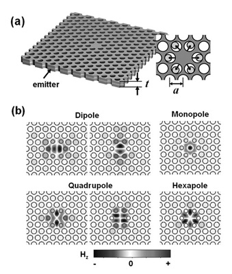
In this section, we review some important characteristics of a few possible resonant modes in a modified single defect PhC cavity.Park et al. (2002) The 3-D FDTD method was employed to analyze optical characteristics such as the mode profile, the factor, the resonant frequency, and so on. A typical structure of the modified single defect cavity and various resonant modes are shown in Fig. 1(a). A free-standing PhC slab structure is assumed as a platform for a triangular PhC lattice. The refractive index of the slab is chosen to be 3.4, which corresponds to that of GaAs around 1 . For real applications, one can insert active semiconductor layers, such as the InAs quantum dots, in the middle of the slab. The air-hole radius and the slab thickness are chosen to be 0.35 and 0.50, respectively, where represents the lattice constant of the triangular PhC. The choice of the slab thickness is important to support only fundamental modes of the slab (TE-like modes).Ryu et al. (2000) Without modification on the nearest air-holes around the defect, only the doubly-degenerate dipole mode can be excited.Painter et al. (1999a, b) However, by reducing the radius of the six nearest air-holes as indicated in Fig. 1(a), other resonant modes within the PBG can be excited. This type of modification was first proposed by Park et al. so as to find a nondegenerate monopole mode used for a photo-pumped low-threshold PhC laser.Park et al. (2001) Especially, as indicated by Ryu et al., the hexapole mode can have a very high value due to the whispering gallery nature of the symmetric field distribution.Ryu et al. (2003) For those modes having an electric-field intensity node at the cavity center, intrinsic properties of those resonant modes is not changed appreciably even after the introduction of a small post at the cavity center. This was a crucial design rule applied for the electrically-pumped PhC laser.Park et al. (2004) One disadvantage of these resonant modes is that the vertical emission is inherently prohibited due to the destructive interference of the anti-symmetric field patterns.
Resonant frequencies and factors of possible resonant modes in the modified single defect cavity are summarized in Table 1. Generally, the total radiated power () can be decomposed into a vertical contribution () and an in-plane contribution ().Painter et al. (1999b) One usually refers to as the inherent optical loss of the resonant mode, because the in-plane loss () can be arbitrary reduced by increasing the number of PhC layer surrounding the cavity. In fact, the factors listed in Table 1 are , which have been obtained by using a sufficiently large horizontal computational domain (). The optical loss of the resonant mode is closely related to the in-plane field distributions. For graphical illustration of the vertical loss, the momentum space intensity distributionSrinivasan and Painter (2002) obtained by Fourier transforming the in-plane field () is calculated. From the in-plane momentum conservation rule, only plane-wave components inside a light-cone [] can couple with propagation modes.
| Dipole | 0.2886 | 14 900 | 46 |
| Quadrupole | 0.3179 | 45 000 | 75.9 |
| Monopole | 0.3442 | 11 000 | 1.2 |
| Hexapole | 0.3149 | 168 000 | 74.5 |
As can be seen from the momentum space intensity distributions of the resonant modes in Fig. 2, the major fraction of the resonant photons live outside the light-cone, which implies an efficient index confinement mechanism. The hexapole mode has negligible plane-wave components inside the light-cone, hence a high factor of 168 000. Among four possible resonant modes, the monopole mode and the dipole mode have relatively low factors ( 10 000). Due to the presence of dc components ( = = 0), the dipole mode shows relatively large radiation losses. Although the controlled vertical emission is essential for good out-coupling, one should not give up the quality factor too much. In fact, several groups have reported high PhC cavities with directional emission.Akahane et al. (2003); Vǔković and Yamamoto (2003); Noda et al. (2002) Later, we will investigate how one can perform additional fine tunings on the modified single defect cavity to obtain both directionality and high .
Finally, we would like to mention how the structural symmetry of the PhC cavity can affect far-field characteristics. The modified single defect PhC cavity depicted in Fig. 1 retains complete six-fold symmetry. The group theory tells us one can classify all the resonant modes into nondegenerate modes and doubly degenerate modes depending on the rotational symmetry; the monopole mode and the hexapole mode are nondegenerate and the dipole mode and the quadrupole mode are doubly degenerate.Kim and Lee (2003); Sakoda (2001) Fig. 3 shows and field distributions of the resonant mode. First, let us look at the case of one of the degenerate dipole modes. In field distribution, due to the odd reflection symmetries by both and , the vertical emission is prohibited. However, in distribution, since all the reflection symmetries are even, there remains a dc component which contributes -polarized vertical emission in the far-field. In the cases of the monopole mode and the quadrupole mode, at least one of the reflection symmetries are odd, thus the vertical emission is always prohibited. In the case of the hexapole mode, field distribution shows even reflection symmetries by both axes ( and ). Considering its perfect six-fold symmetry, field components must be completely balanced to give a zero dc component. Thus, field distribution reveals that such delicate balance can be easily broken by introducing a small structural perturbation, resulting in nontrivial vertical emission. We will discuss this type of defect engineering in Sec. IV.
III Far-field simulation
III.1 Far-field simulation method
To obtain the far-field radiation pattern, we should deal with the radiation vectors that are sufficiently far () from a light emitter.Jackson (1974) Direct application of the FDTD method would be difficult because of the limited computer memory size and time. Here, we shall explain how one can efficiently obtain the far-field radiation by combining the 3-D FDTD method and the near- to far-field transformation formulae. This method has been well known in the field of electronics since 1980s dealing with antenna radiation problems. Vǔković et al. applied the FFT-based far-field simulation algorithm to their factor optimization of the PhC cavity mode.Vǔković et al. (2002)
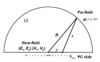
We explain the basic concept of the efficient far-field computation in Fig. 4. Here, we divide the whole calculation domain by a horizontal plane located just above the PC slab. The upper domain is bounded by an infinite hemisphere. All field components ( and ) are assumed to fall off as , typical of radiation fields. It is also assumed that in-plane field components (, , , and ) detected at the horizontal plane decay exponentially as the horizontal distance . According to the surface equivalence theorem, for the calculation of the fields inside an imaginary closed space , the equivalent electric () and magnetic () currents on the surrounding surface can substitute all the information on the fields out of the , where and are calculated by using the following formulae.
| (1) | |||
| (2) |
Here, is a unit normal vector on the surface. Neglecting the fields on the hemisphere, only the in-plane field data detected at the horizontal plane will be used for the far-field computation. Then, these equivalent currents are used to obtain the following retarded vector potentials.
| (3) | |||
| (4) |
In the far-field regime, (), the above formulae can be simplified as
| (5) | |||
| (6) |
Using a relation , the radiation vectors and are simply related by 2-D FTs.
| (7) | |||
| (8) |
and components of the radiation vectors can be represented as
| (9) | |||
| (10) | |||
| (11) | |||
| (12) |
Then, far-field radiation patterns are obtained by calculating time-averaged Poynting energy per unit solid angle.Jackson (1974)
| (13) |
where is the impedance of free space.
One can easily implement this algorithm into the FDTD code. During the FDTD time stepping, the in-plane field data (near-field data) that contain complete information on the far-field are obtained. Once the FDTD computation is completed, the radiation vectors ( and ) are calculated by the FTs. Then, these radiation vectors are used to obtain far-field patterns according to Eq. (13). One can use the 2-D FFT algorithm for efficient FT computations [see Eqs. (9)-(12)]. In our FDTD simulation, the size of the computational grid was ( is the lattice constant), and the size of the horizontal calculation domain were . Thus, each in-plane field data will contain approximately data points. In the FFT algorithm, input data are transformed to the output matrix data with the same size, where is .Press et al. (1992) Assume that unit cells in the data correspond to a spatial length of wavelengths (). The frequency step is and the maximum frequency is thus . Thus, the value of the light-cone corresponds to the Lth point in the frequency space. Note that only the wavevector components lying inside the light-cone whose radius is cells can contribute to the outside radiation. To increase the resolution of the far-field simulation, one should increase the horizontal size of the FDTD domain. Fortunately, there is an easy way to do so without performing an actual calculation in the larger FDTD domain. We can enlarge the input matrix data by filling null (0) values, for example, into size matrix. Such arbitrary expansion is legitimate since most of the near-field energy of a PhC cavity mode is strongly confined around the central defect region. When the normalized frequency of a PhC cavity mode is (typical of PhC defect modes), = 2048 cells = 102.4 (). Thus, the resultant far-field data resolution is .
Finally, we would like to mention one more before presenting calculated far-field patterns. All and data described in the above formulae are phasor quantities. Thus, when we detect the in-plane field data, we have to extract both amplitude and phase information, because, in general, phases will change differently at each position. The situation containing the bottom reflector is the case, where the reflected waves can no longer be described as a simple standing wave of . Assuming a single mode , all field vectors in the simulation should have the following form.
| (14) |
An efficient method to obtain the exact phasor quantities is to incorporate recursive discrete FTs (DFTs) concurrently with the FDTD time stepping.
| (15) | |||
| (16) |
Here, to obtain real () and imaginary () components of field, simple recursive summations are performed on each grid point () at the FDTD time . Note that the above formulae correspond to the following Fourier transformation.
| (17) |
In general, this summation should continue until the field values ‘ring down’ to zero. However, in the case of high factor resonant mode, by carefully exciting a dipole source (source position and frequency), small FDTD time steps (usually 20 000 30 000 FDTD time steps, or equivalently 200 optical periods) are sufficient to obtain nearly exact phasor quantities. In the next section, we will show calculated far-field patterns.
III.2 Far-field simulation results
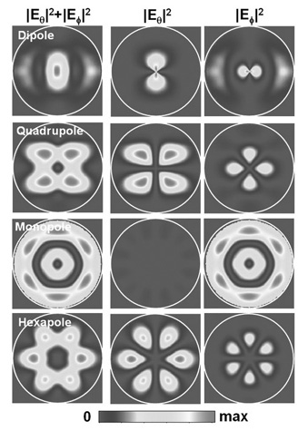
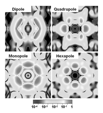
To calculate the far-field pattern, we have used the 3-D FDTD method and the near- to far-field transformation algorithm which has been outlined in the previous subsection. The horizontal calculation domain of and the spatial grid resolution of were used. Calculated far-field patterns are shown in Fig. 5. All the far-field data () shown in this article are represented by using a simple mapping defined by and . Depending on the rotational symmetry that the each resonant mode has, the far-field pattern also shows several regularly spaced lobes, which in turn explain the labeling of these modes; Number of lobes in the far-field pattern are four (six) in the case of the quadrupole mode (the hexapole mode). Ignoring weak intensity modulation laid upon dominating circular emission pattern, the monopole mode shows two concentric ring-shape patterns, which show indeed a monopole-like oscillation. In fact, emission patterns of the hexapole mode and the monopole mode does not bear perfect six-fold symmetry, e.g. two horizontal lobes look bigger than the others in the case of the hexapole mode. These discrepancies are due to rectangular grids of the FDTD computation cell which are not well matched with the six-fold symmetric case. (Later, we will explain more in detail.) Along with total intensity () patterns, we also display theta-polarized intensity () patterns and phi-polarized intensity () patterns. Note that such polarization-resolved far-field data can be easily obtained in the real measurement setup (a solid angle scanner) by placing a polarizer in front of a photo-detector which scans the whole hemispherical surface.Shin et al. (2002)
First, let us look at the results of the quadrupole mode. Comparing with the total intensity power, it can be deduced that most of the emitted power is theta-polarized. Also in the case of the hexapole mode, theta-polarized emission seems to dominate phi-polarized one. Table 1 summarize percentages of the theta-polarized power and the phi-polarized power. As expected, the quadrupole mode and the hexapole mode are almost theta-polarized (). However, the monopole mode shows opposite result; phi-polarized emission dominates by . As indicated by Povinelli et al., one may create an artificial magnetic emitter by using the monopole-like mode which shows the same emission characteristics reminiscent of those of the magnetic multipole.Povinelli et al. (2003) Considering that electric (magnetic) dipole radiation is theta-polarized (phi-polarized),Jackson (1974) such polarization characteristics seem to be closely related with composition of the electric multipoles and the magnetic multipoles. Thus, the so called multipole decomposition could provide other perspectives for various radiation properties of PhC nanocavities along with the plane-wave decomposition (FT based analyses).
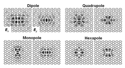
From polarization-resolved far-field patterns, it looks as if the dipole mode has a certain singularity near the north pole (). This feature comes from the strongly -polarized dipole mode. Upon inspection of the region around the vertical, one can observe that directions of the electric field vectors indeed predominantly lie in the direction. Fig. 6(a) shows the -polarized emission pattern () and the -polarized emission pattern (). The result shows the domination of the -polarized emission over the -polarized one.Painter and Srinivasan (2002) Thus, except the inherent degeneracy, the dipole mode itself can be a good candidate for the vertical emitter.
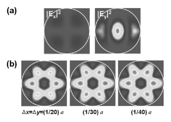
Finally, we would like to mention the origin of the unevenness for the six lobes in the far-field patterns of the hexapole mode and the monopole mode. These symmetry-breaking comes from the rectangular grid, used in the FDTD computation, which does not fit in the hexagonal symmetry. To check this point, we re-calculated the far-field pattern of the hexapole mode with the grid of the finer grid resolution. In this computation, was fixed and only the horizontal grids () were changed. Fig. 6(b) shows that, by increasing the horizontal grid resolution, the far-field pattern restores the inherent six-fold symmetry. This comparison confirms that such unbalanced lobes are attributable to the rectangular FDTD grid. Note that even in case of , all important features of the radiation can still be obtained except the slight unevenness. Thus, all the calculations in Sec. IV were performed with the grid resolution of .
IV Engineering radiation properties
IV.1 Defect engineering
As discussed, the in-plane field distribution determines the far-field radiation pattern. In this subsection, we will investigate how the defect engineering method can be applied to manipulate the radiation profile. The hexapole mode depicted in Sec. II shows null vertical emission due to the symmetric field distribution which has a zero dc component. However, as discussed in the last part of Sec. II, it seems that the field balance can be easily broken by introducing small structural perturbation. As shown in Fig. 7(a), the structural tuning that we have applied is to enlarge two horizontal air-holes facing with each other.Kim (a) From the hexapole mode field distribution shown in Fig. 3, it can be expected that such perturbation will break the delicate balance of the distribution. Note that noticeable amount of the dc component appears in the .Kwon
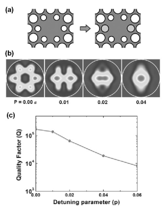
In Fig. 7(b), the far-field patterns are plotted as we increase the air-hole radius. Here the same structural parameters used in Fig. 1 are assumed. One can clearly observe how the hexagonally-distributed pattern is transformed into the directional beaming. The radiation pattern becomes more directional with the air-hole radius. When the air-hole radius increment is , the vertical emission looks most favorable. In this case, of the total radiated energy falls within the collection angle of . In other words, of the total emitted photons can be collected from the top. The downward photons could be re-directed by introducing a reflector underneath. In the next section, we shall discuss the efficient unidirectional beaming strategy based on the defect tuning and the bottom reflector. The factors of the proposed hexapole mode are presented in Fig. 7(c). The exponential decrease of the factor is observed as a function of the detuning parameter (). Note that when the , the factor is still not too bad, 20 000.
Since the above modification of two air holes breaks mostly the balance of the field and not that of the field, the directional beaming obtained here will be almost -polarized. Fig. 8(a) shows the polarization-resolved far-field patterns, where such directional beaming is clearly -polarized. With the same numerical aperture of the lens (0.5) used previously, the polarization extinction ratio is estimated to be . Therefore, we claim that both the directionality and the linear polarization can be obtained from the hexapole mode by introducing small structural perturbation. However, by the same token, this result implies that the hexapole mode in the modified single defect cavity is not robust against the structural perturbation, because the electric fields are concentrated in the proximity of the nearest air-holes. This fact also explains one of the reasons why the observed factors of the hexapole mode are much smaller than the values obtainable in the FDTD computation .Ryu et al. (2003); Kim (b) Recently the other class of hexapole modes that are robust against the perturbation was also found, where the electric field energy is concentrated in the dielectric region between the nearest air-holes.Kwon ; Kim et al. (2005)
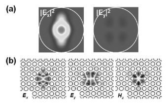
Finally, it should be noted that the near-field distribution of the deformed hexapole mode is almost identical to that of the ideal hexapole mode and retains the whispering-gallery-like nature. Remember that the , , and field components shown in Fig. 8(b) is the results obtained after only very slight modification of the holes (). It is interesting that the resulting far-field pattern can be changed drastically by such minute perturbation. Thus, as indicated by Shin et al. a thorough understanding of wavelength-size small cavities requires investigations in the both regimes; the near-field and the far-field.Shin et al. (2002)
IV.2 Effects of the bottom reflector
Purcell claimed that the spontaneous emission lifetime is a constant that can be altered depending on the optical mode density and the electric-field intensity near the emitter .Purcell (1946) Borrowing this concept, it can be said that inherent radiation properties of the PhC slab resonant mode should be modified by placing a reflector near the cavity.Björk et al. (1991) In the early days, researchers used PhC resonant cavities as a vehicle to study the alteration of spontaneous emission .Hwang et al. (1999); Lee et al. (2000); Ryu and Notomi (2000) For example inside the periodic structure, the spontaneous emission can be suppressed for a certain frequency range (PBG) or enhanced for a particular frequency. As will be shown below, one can further modify the resulting radiation properties from the PhC cavity by using a flat-surface mirror.Hinds (1994)
The PhC slab structure to be investigated here is shown in Fig. 9. The proposed structure is very simple; it consists of a PhC slab and a bottom reflector. As a reflector, a simple dielectric substrate or a Bragg mirror is to be used. Such a structure is realistic since the thickness of each layer can be controlled during the wafer growth. We note that similar planar systems were studied by SchubertSchubert et al. (1992) and BenistyBenisty et al. (19982) in an attempt to alleviate the poor light extraction efficiency of microcavity LEDs. To investigate effects of the presence of the bottom reflector, we have calculated the change of factors and far-field radiation patterns as we vary the air-gap distance between the PhC slab and the bottom reflector (see Fig. 10). Here, the factor represents the lifetime of the resonant mode (). As a PhC resonant mode, the quadrupole mode shown in Fig. 5 is used. As a bottom reflector, we assumed a simple dielectric substrate whose refractive index is 3.4.
Compared with the original far-field pattern shown previously in Fig. 5, the radiation profile shown in Fig. 10 changes noticeably with the air-gap size. The far-field patterns show the signature of concentric ring-shape modulation laid upon the original far-field pattern, which is reminiscent of the Fabry-Pérot fringes Born and Wolf (1980) in the Fabry-Pérot etalon. Although the reflectivity of the bottom GaAs (or InP) substrate is only , the interference between the original wave and the reflected wave is easily noticeable. Upon inspection of the far-field patterns in Fig. 10(a), one can find that the similar far-field patterns show up again after the air-gap increment of (for example, compare and ). This increment corresponds to around a half-wavelength (). It should be noted that the directional beam cannot be achieved from the quadrupole mode. To achieve unidirectional emission, we need to investigate the inherently directional resonant mode such as the deformed hexapole mode.
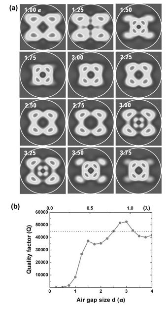
Similar systematic dependence on the air-gap size is also observed in the factor of the resonator, at a period of approximately . Note that the factor decreases drastically when the air-gap size becomes less than . There are two distinct reasons for this phenomenon; one is the TE-TM coupling loss through the PhC slab Tanaka et al. (2003) and the other is the diffraction loss in the downward direction. The TE-TM coupling loss always occurs when the vertical symmetry of the PhC slab structure is broken. The reason for the increase of the diffraction loss to the downward direction is that the light-cone of the bottom substrate is effectively enlarged by a factor of (the refractive index of the substrate). When the bottom substrate is too close from the slab, the tail of the evanescent field begins to feel the substrate. Such an expanded light-cone will allow the more plane-waves to be coupled to substrate-propagating modes. Therefore, in order to prevent this loss, the air-gap size larger than is generally recommended. It is interesting to find that the factor can be enhanced even in the presence of the bottom substrate. In fact, when the air-gap size is larger than , the factor oscillates around the original value. Note that the interference phenomena observed here are similar to the cases of the dipole antenna placed near an ideal plane mirror.Hinds (1994)
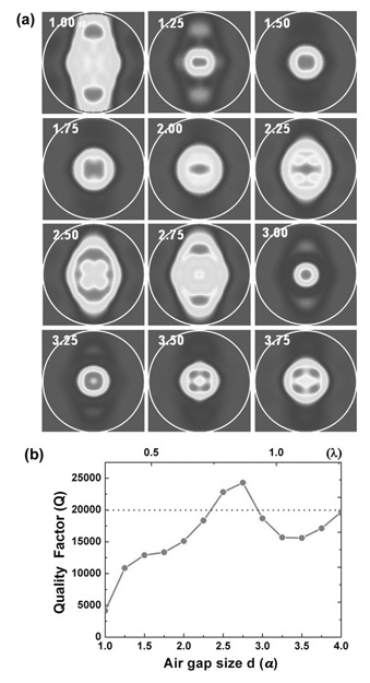
The case of the deformed hexapole mode is worth special attention. Fig. 11(a) shows the far-field radiation patterns with a perturbation parameter (see Fig. 7). The same bottom substrate of index 3.4 is used. Here again, one can see that the original far-field patterns are modified by concentric ring-shape modulations. Comparing the patterns of and , one can witness that the similar vertical enhancement is restored after the air-gap is increased by additional thickness of . This air-gap thickness corresponds to, approximately, a half-wavelength (). At this point, the vertical enhancement condition seems to be summarized as , where is the air-gap size and integral multiple. Moreover, the air-gap size of where the good directionality is obtained is approximately equal to one wavelength (). If one wants to find the rigorous conditions of optimal vertical enhancement, the analyses need to include the effects of the optical thickness of the PhC slab and the phase change upon reflection. In the next section, we shall develop a simple, plane-wave based interference model to explain the vertical enhancement conditions. From the factors, one can clearly see, again, the modification of the intrinsic radiation lifetime, where the oscillation period around the dotted line is [See Fig. 11(b)]. Note that there seems to be no definite relation between the factor optimization and the vertical enhancement condition; The optical loss of the cavity () is a result of the sum of the emitted power (). A simple guess of the by the emission pattern itself can be misleading.
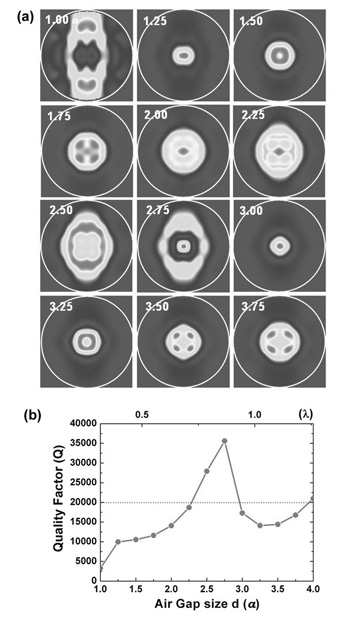
In principle, one can completely block the downward propagating energy by using a highly-reflective Bragg mirror. For example, a stack of 25 AlAs/GaAs pairs give a reflectivity in excess of 0.998.Coldren and Corzine (1995) In the subsequent analyses, we will use a Bragg mirror made of a stack of 20 AlAs/GaAs pairs whose reflectivity is . Remember that the FDTD grid resolution for the direction [] is, in fact, not sufficiently fine to fully describe the each Bragg layer (around 10 grids are used to describe one pair of AlAs/GaAs).Taflove and Hagness (2000) As a result, the reflectivity would be slightly smaller than the actual value.
Far-field patterns in presence of a Bragg mirror are collectively shown in Fig. 12(a). In comparison with Fig. 11(a), the concentric ring-shape modulation is more pronounced due to the high reflectivity of the bottom structure. In the factor plot shown in Fig. 12(b), the modification of the radiation lifetime is also prominent. The maximum factor is increased from 25 000 to 35 000, which represents an increase of the radiation lifetime by in comparison with that without a reflector. Note that, except for such increased interference effects, all other characteristic features in the far-field patterns still remain almost unchanged. In short, we confirmed that both the radiation lifetime and the radiation pattern can be controlled by simply adjusting the distance between the PhC slab and the reflector. As shown in the far-field pattern of , one can achieve a sharp directional emission in which most of the emitted power () is concentrated within .
IV.3 Design rule for directional emission
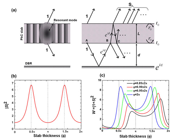
In the preceding subsection, we have shown that, by using the 3-D FDTD method and the near- to far-field transformation algorithm, the radiation patterns of the PhC defect modes can be altered by the bottom reflector. Especially the choice of air-gap seems to give the best directional emission. In this subsection, we will try to find conditions for the directionality, by developing a simple analytic model based on plane-wave interferences.
We assume that the PhC slab can be approximated as a uniform dielectric slab having an effective refractive indexFan and Joannopoulos (2002) and the PhC resonant mode can be treated as a point dipole source embedded in the middle of the slab and the radiations are described by scalar plane-waves. We also assume that the bottom reflector is positioned sufficiently far () from the PhC slab. The reflector does not perturb too much the original characteristics of the resonant mode. Thus, the initially upward and downward propagating waves (See Fig. 13(a)) can be assumed to be symmetric, 1 and 1. The downward propagating component will eventually be redirected upward to make an interference with the upward propagating component. Although these assumptions seem to be very simple, similar approaches based on the plane-wave interferences have already been used for the calculation of radiation patterns of atomic dipoles in a planar microcavity.Benisty et al. (19982); Dowling et al. (1991) As indicated by DowlingDowling et al. (1991), the mode structure of the electromagnetic field is a classical phenomenon.
In the simplest case when multiple reflections between the PhC slab and the bottom reflector can be neglected 111When an optical thickness of a PhC slab is ‘slab resonance condition’, the PhC slab becomes transparent (zero reflectance)., a constructive inteference condition at the vertical becomes
| (18) |
where is a round-trip phase in the air-gap. and are the phase changes at the bottom reflector 222When we use a Bragg mirror as a bottom reflector, a reflection phase is at the Bragg frequency. This phase shift is the same with the case of a perfect conducting mirror. and through the PhC slab, respectively (See Fig. 13(a)). When the radiation into an angle is considered,
| (19) | |||||
| (20) |
where and are the air-gap thickness and the slab thickness, respectively. Considering the typical thickness of the PhC slab of , one may assume .Johnson et al. (1999) Then, Eq. (18) becomes
| (21) |
This condition is consistent with the previous observation () which has been deduced from the far-field patterns. However, in general, the PhC slab thickness does not satisfy this ‘slab resonance condition ()’ and the residual reflection can not be completely cancelled. Then, what should be changed in the vertical enhancement conditions [Eq. (18)] when multiple reflections become significant?
Fig. 13(a) describes the situation where the emission from the cavity is divided by the upward and the downward propagating waves. Here, we focus only on the vertical interference conditions (). and are coefficients of amplitude reflection and transmission for a single dielectric interface, respectively. Let be the sum of all the waves detected upward which initially propagate downward. Then, an interference between the originally upward propagating wave and the will be described by , and the resultant intensity will be proportional to . To sum all the waves which undergo infinitely many multiple reflections in the slab and in the air-gap, we introduce a simple method which take advantage of the similarity of such multiple reflections and transmission.
We trace several reflections and transmissions of the wave which start out at point in the initial stage. At point , the wave is divided into two. Here, the downward propagating component will undergo the same multiple reflections as the wave at . Let be the sum of all the waves detected upward which propagate upward at , then we get the following equation for the .
| (22) |
Now, let us proceed the upward propagating wave at more. The wave once reflected at the top of the slab will reach at point , there, two divided waves have resemblance to the waves which contribute to the and the , respectively. Describing these processes,
| (24) |
Now, let us examine two representative cases of the PhC slab;
‘slab resonance’ and ‘slab antiresonance’.
(1) Slab Resonance
This is a case when , i.e., . From the well known result for the transmittance in a uniform dielectric slab,Coldren and Corzine (1995) we know that the slab becomes transparent and multiple reflections in the air-gap do not occur. Thus, we can easily guess that this case restores the simplest two-beam interference result dealt in Eq. (18). By inserting into the Eq. (24), we get
| (25) |
Resultant radiation intensity becomes
| (26) |
This is the famous two-beam interference formula, if the phase change at the bottom mirror is , then the condition for a constructive interference becomes
| (27) |
The maximum radiation intensity is with the above
condition.
(2) Slab Antiresonance
This is a case when , i.e., . The reflectance from the dielectric slab is maximized with this slab thickness. Inserting into Eq. (24),
| (28) |
Here, we let again be , then one can easily prove that the condition of the air-gap to maximize is (air-gap resonance).
| (29) |
Assuming the effective refractive index of the slab () by 2.6, then . The vertical radiation intensity becomes
| (30) |
which can be larger than that of the slab resonance. Note that the
condition for maximizing is slightly different from the slab
antiresonance, because of a phase difference between two complex
numbers ( is a pure imaginary while ‘’ is a real).
In Fig. 13(c), we plot as a function of the slab thickness () for various air-gap sizes (). A blue line represents the result when the air-gap size exactly equals the emission wavelength (). Other lines represent the air-gaps as indicated. Here, it is found that 1) the overall emission intensity decreases as the air-gap is detuned from the ‘’ condition and 2) when the air-gap size is ‘’(on-resonance), there exists a relatively wide concave plateau in the neighborhood of the ‘slab resonance’ (). In this case, the vertical emission is enhanced by a factor larger than 4, over a wide range of slab thicknesses. Although the better vertical enhancement can be obtained near the ‘slab antiresonance’ (), the thickness of the PhC slab is better to be chosen near the ‘resonance’ condition, because the thicker slab tends to support unwanted higher-order guided modes.Ryu et al. (2000) Thus, thanks to the multiple reflection effect, the vertical enhancement condition now becomes rather simple. Above analyses suggest that the focus should be placed more on the air-gap size that has be exactly matched with the emission wavelength than on the PhC slab thickness that is already designed near the antiresonance condition.
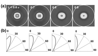
To confirm the above argument, we have calculated far-field patterns of the deformed hexapole mode using the ‘’ air-gap. We have increased the slab thickness from to , which correspond to approximately the phase thickness from to 333Optical thicknesses of the PhC slab are estimated from the transmittance spectrum which has been obtained by using the 3-D FDTD method with periodic boundary conditions. For references, see Fan et al. Fan and Joannopoulos (2002). Since resonant mode frequencies are changed by the slab thickness, the air-gap sizes have been adjusted to fit the ‘’ condition. As shown in Fig. 14, good directional patterns are obtained. It is interesting to note that the far-field pattern becomes more directional as the slab thickness increases. Therefore, as expected in the previous argument, the slab slightly thicker than that satisfying the resonance condition is preferable for the enhanced vertical beaming. From the far-field pattern of , it is found that more than of the emitted power is contained within an angle of .
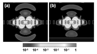
Figure 15 shows the electric-field intensity
distributions detected in the - plane. For comparison, the
case of a symmetric PhC slab cavity without a bottom reflector is
also shown. In Fig. 15(b), one can clearly see that
the downward propagating waves are effectively redirected by the
Bragg mirror and the unidirectional emission is achieved. In other
words, we have shown that inherent radiation patterns of the PhC
slab resonant mode can be controlled either by modifying the
defect structures, or by placing a reflector near the cavity. By
simply adjusting the air-gap size to be , one can obtain
fairly good directional patterns. The directionality improves
continuously until the slab thickness becomes near the slab
antiresonance. In a practical point of view, the air-gap size is a
fixed quantity which cannot be changed after the wafer growth
444Recently, LEOM group in France has demonstrated
PC-MOEMS, where one can control the air-gap size by using
electro-static force. See, for instance, J. L. Leclercq, B.
BenBakir, H. Hattori, X. Letartre, P. Regreny, P. Rojo-Romeo, C.
Seassal, P. Viktorovitch, Proc. SPIE, 5450, 300 (2004).. Thus,
the most important design rule for the directional emission is to
choose the air-gap size (thickness of a sacrificial layer) to be a
target wavelength ‘’. Then, the remaining critical issue
will be that of the lithographic tuning that matches the resonant
wavelength of the mode of interest with the emission wavelength of
quantum well or quantum dots.
V Summary
We have shown that the radiation pattern and the radiation lifetime of the 2-D PhC slab resonant mode can be controlled by placing a mirror near the cavity. To calculate the far-field pattern, we have developed a simple and efficient simulation tool based on the FDTD method and the near- to far-field transformation. We have discussed two distinct physical mechanisms responsible for the modification of the far-field radiation pattern. Either by tuning the defect structure or by placing a reflector near the cavity, we have shown that the unidirectional emitter whose energy is concentrated within a small divergence angle () can be achieved. Simple plane-wave based interference model has revealed that the vertical enhancement condition is satisfied when the air-gap size is equal to the emission wavelength. To further enhance the directionality, the slightly thicker PhC slab design than the ‘slab resonance’ condition would be recommended. The proposed structure is practical since the critical design parameter can be precisely controlled during the epitaxial growth.
Acknowledgements.
One of the authors, S. H. Kim, would like to thank S. H. Kwon, M. K. Seo, J. K. Yang for their valuable assistance and discussions. S. H. Kim would also like to thank J. M. Gérard in CEA in France for his valuable discussions. This research was supported by a Grant from the Ministry of Science and Technology (MOST) of Korea.References
- Joannopoulos et al. (1997) J. D. Joannopoulos, P. R. Villeneuve, and S. Fan, Nature (London) 386, 143 (1997).
- Johnson et al. (1999) S. G. Johnson, S. Fan, P. R. Villeneuve, J. D. Joannopoulos, and L. A. Kolodziejski, Phys. Rev. B 60, 5751 (1999).
- Kim et al. (2004) S. H. Kim, G. K. Kim, S. K. Kim, H. G. Park, Y. H. Lee, and S. B. Kim, J. Appl. Phys. 95, 411 (2004).
- Painter et al. (1999a) O. Painter, R. K. Lee, A. Yariv, A. Scherer, J. D. O’Brien, P. D. Dapkus, and I. Kim, Science 284, 1819 (1999a).
- Park et al. (2001) H. G. Park, J. K. Hwang, J. Huh, H. Y. Ryu, Y. H. Lee, and J. S. Kim, Appl. Phys. Lett. 79, 3032 (2001).
- Ryu et al. (2002a) H. Y. Ryu, S. H. Kwon, Y. J. Lee, Y. H. Lee, and J. S. Kim, Appl. Phys. Lett. 80, 3476 (2002a).
- Akahane et al. (2003) Y. Akahane, T. Asano, B. S. Song, and S. Noda, Nature (London) 425, 944 (2003).
- Ryu et al. (2003) H. Y. Ryu, M. Notomi, and Y. H. Lee, Appl. Phys. Lett. 83, 4294 (2003).
- Yoshie et al. (2004) T. Yoshie, A. Scherer, J. Hendrickson, G. Khitrova, H. M. Gibbs, G. Rupper, C. Ell, O. B. Shchekin, and D. G. Deppe, Nature (London) 432, 200 (2004).
- Gérard and Gayral (2004) J. M. Gérard and B. Gayral, Proc. SPIE 5361, 88 (2004).
- Vǔković and Yamamoto (2003) J. Vǔković and Y. Yamamoto, Appl. Phys. Lett. 82, 2374 (2003).
- Hennessy et al. (2004) K. Hennessy, A. Badolato, P. M. Petroff, and E. Hu, Photonics and Nanostructures (Elsevier) 2, 65 (2004).
- Park et al. (2004) H. G. Park, S. H. Kim, S. H. Kwon, Y. G. Ju, J. K. Yang, J. H. Baek, S. B. Kim, and Y. H. Lee, Science 305, 1444 (2004).
- Noda et al. (2002) S. Noda, M. Imada, M. Okano, S. Ogawa, M. Mochizuki, and A. Chutinan, IEEE J. Quantum Electron. 38, 726 (2002).
- Asano et al. (2003) T. Asano, M. Mochizuki, S. Noda, M. Okano, and M. Imada, IEEE J. Lightwave Technol. 21, 1370 (2003).
- Noda et al. (2000) S. Noda, A. Chutinan, and M. Imada, Nature (London) 407, 608 (2000).
- Takano et al. (2004) H. Takano, Y. Akahane, T. Asano, and S. Noda, Appl. Phys. Lett. 84, 2226 (2004).
- Park et al. (2002) H. G. Park, J. K. Hwang, J. Huh, H. Y. Ryu, S. H. Kim, J. S. Kim, and Y. H. Lee, IEEE J. Quantum Electron. 38, 1353 (2002).
- Ryu et al. (2002b) H. Y. Ryu, H. G. Park, and Y. H. Lee, J. Sel. Top. Quantum Electron. 8, 891 (2002b).
- Coldren and Corzine (1995) L. A. Coldren and S. W. Corzine, Diode Lasers and Photonic Integrated Circuits (Wiley, New York, 1995).
- Taflove and Hagness (2000) A. Taflove and S. C. Hagness, Computational Electrodynamics: the finite-difference time-domain method (Artech House, Norwood, MA, 2000), 2nd ed.
- Vǔković et al. (2002) J. Vǔković, M. Lončar, H. Mabuchi, and A. Scherer, IEEE J. Quantum Electron. 38, 850 (2002).
- Ryu et al. (2000) H. Y. Ryu, J. K. Hwang, and Y. H. Lee, J. Appl. Phys. 88, 4941 (2000).
- Painter et al. (1999b) O. J. Painter, A. Husain, A. Scherer, J. D. O’Brien, I. Kim, and P. D. Dapkus, IEEE J. Lightwave Technol. 17, 2082 (1999b).
- Srinivasan and Painter (2002) K. Srinivasan and O. Painter, Opt. Express 10, 670 (2002).
- Kim and Lee (2003) S. H. Kim and Y. H. Lee, IEEE J. Quantum Electron. 39, 1081 (2003).
- Sakoda (2001) K. Sakoda, Optical Properties of Photonic Crystals (Springer-Verlag, Berlin Heidelberg, 2001).
- Jackson (1974) J. D. Jackson, Classical Electrodynamics (Wiley, New York, 1974).
- Press et al. (1992) W. H. Press, B. P. Flannery, S. A. Teukolsky, and W. T. Vetterling, Numerical Recipes in C: The Art of Scientific Computing (Cambridge University Press, 1992), 2nd ed.
- Shin et al. (2002) D. J. Shin, S. H. Kim, J. K. Hwang, H. Y. Ryu, H. G. Park, D. S. Song, and Y. H. Lee, IEEE J. Quantum Electron. 38, 857 (2002).
- Povinelli et al. (2003) M. L. Povinelli, S. G. Johnson, J. D. Joannopoulos, and J. B. Pendry, Appl. Phys. Lett. 82, 1069 (2003).
- Painter and Srinivasan (2002) O. Painter and K. Srinivasan, Opt. Lett. 27, 339 (2002).
- Kim (a) S. K. Kim, (unpublished).
- (34) S. H. Kwon, (unpublished).
- Kim (b) G. H. Kim, (private communication).
- Kim et al. (2005) S. K. Kim, J. H. Lee, S. H. Kim, I. K. Hwang, Y. H. Lee, and S. B. Kim, Appl. Phys. Lett. 86, 031101 (2005).
- Purcell (1946) E. M. Purcell, Phys. Rev. 69, 681 (1946).
- Björk et al. (1991) G. Björk, S. Machida, Y. Yamamoto, and K. Igeta, Phys. Rev. A 44, 669 (1991).
- Hwang et al. (1999) J. K. Hwang, H. Y. Ryu, and Y. H. Lee, Phys. Rev. B 60, 4688 (1999).
- Lee et al. (2000) R. K. Lee, Y. Xu, and A. Yariv, J. Opt. Soc. Am. B 17, 1438 (2000).
- Ryu and Notomi (2000) H. Y. Ryu and M. Notomi, Opt. Lett. 28, 2390 (2000).
- Hinds (1994) E. A. Hinds, in Cavity Quantum Electrodynamics (Academic Press, Inc, Orlando, 1994), edited by P. R. Berman.
- Schubert et al. (1992) E. F. Schubert, Y. H. Wang, A. Y. Cho, L. W. Tu, and G. J. Zydzik, Appl. Phys. Lett. 60, 921 (1992).
- Benisty et al. (19982) H. Benisty, H. D. Neve, and C. Weisbuch, IEEE J. Quantum Electron. 34, 1612 (19982).
- Born and Wolf (1980) M. Born and E. Wolf, Principles of Optics (Cambridge University Press, 1980), pp. 329,330.
- Tanaka et al. (2003) Y. Tanaka, T. Asano, Y. Akahane, B. S. Song, and S. Noda, Appl. Phys. Lett. 82, 1661 (2003).
- Fan and Joannopoulos (2002) S. Fan and J. D. Joannopoulos, Phys. Rev. B 65, 235112 (2002).
- Dowling et al. (1991) J. P. Dowling, M. O. Scully, and F. DeMartini, Opt. Commun. 82, 415 (1991).