address=Department of Physics, University of California, Riverside, CA92521, USA, altaddress=KFKI RMKI, Konkoly Thege Miklós út 29-33, Budapest, H-1121, Hungary
The CMS Silicon Strip Tracker
Abstract
The CMS collaboration is constructing the largest silicon tracker ever built with an active silicon area of 200 m2 to provide robust charged particle tracking and vertex reconstruction within the 4T magnetic field of the CMS Solenoid. The design of the detector, the status of the construction and the performance of the substructures are reviewed.
:
29.40.Wk, 29.40.Gx, 01.30.Cc1 The CMS Silicon Strip Tracker
The CMS Tracker is composed of a Silicon Pixel Detector and a large volume Silicon Strip Tracker (SST). The CMS SST cms-sst consists of 15148 modules housing 24244 silicon strip sensors and their front-end electronics with 9.6 million readout channels in total. The modules are mounted on local support structures in four distinct subsystems: the Inner and Outer Barrels, the two Inner Disks and the two End-Caps. The Inner Barrel is composed of four and the Outer Barrel of six cylindrical layers. Each Inner Disk is made of three disks, each divided into three rings, while the End-Caps have nine disks with four to seven rings. Typically 10 points are measured along the track up to a rapidity of 2.4. The regions and cm are populated by double sided modules constructed by mounting two independent single sided modules back to back with a stereo angle of 100 mrad. The SST will be housed inside a 5.4 m long and a 2.4 m diameter cylindrical support tube and an active thermal shield will keep the volume at a temperature below -10 C and at a relative humidity of 30%.
2 Module and component production
The basic building blocks of the SST are the modules. Each module has 1 or 2 silicon sensors mounted on a carbon-fiber or graphite support frame with a kapton circuit to isolate the silicon backplane and supply the bias voltage. The readout and control chips are mounted on the front-end (FE) hybrid. A glass circuit, the pitch adapter, provides fan-out from the sensors with a pitch of 80-205 m to the readout chips. In total about 25M micro-bonds provide the electrical connection between the module parts. To comply with the mechanical constraints there are 29 different module types using 16 different single-sided sensor, 12 FE hybrid and 26 pitch adapter designs.
Sensors sensor are fabricated on 6” wafers using non-oxygenated n-type bulk with ¡100¿ lattice orientation and have 512 or 768 p+ strip implants with a width/pitch ratio of 0.25. In the barrel region, rectangular sensors are mounted with strips parallel to the beam axis, while in the End-Caps and Inner Disks, wedge-shaped sensors with strips in the radial direction. In the inner region ( cm) one 320 m thick, low resistivity (1.5-3.5 kcm) sensor is housed on a module, while in the outer region two 500 m thick, high resistivity (3.5-7.5 kcm) sensors are daisy-chained.
During the production of the thick sensors a large number of problems were encountered, most notably a deep corrosion of the sensors sensor-corrosion . This forced us to shift most of the order to the producer of the thin sensors.
The front-end (FE) hybrid is realized as a four-layer kapton substrate laminated on a ceramic carrier and having a flex tail for electrical connections. It houses 4 or 6 APV25 readout chips made by IBM’s radiation hard 0.25 m CMOS technology. The APV25 has two operation modes: the peak mode where the output sample corresponds to the peak amplitude, and the deconvolution mode that makes a weighted sum of three consecutive samples and allows for the identification of the correct bunch crossing in the high luminosity phase of LHC.
Several problems occurred during the FE hybrid mass production, the most serious of which was the discovery of broken vias which turned out to be inherent to the design and the production method. The FE hybrid originally was built up from two kapton circuits glued together. During the laser drilling of the 100 m vias, the glue melted faster, potentially forming a cavity which then lead to very poor metalization of the via. This problem was solved by introducing a third kapton layer and by increasing the via diameter from 100 to 120 m. Throughout the production, the long-term reliability of the micro-bonds between the APV25 and the substrate due to over-deformation of the bond feet and the occurrence of cratering was also a concern.
All modules are built and tested in the collaborating institutes with automatized, computer-controlled procedures, including a high-precision robotic assembly of the modules at six production centers and wire bonding using more than 20 bonding machines. The modules are tested on fast single module setups based on the APV Readout Controller (ARC) and then on long-term test stands with a CMS-like DAQ system executing several thermal cycles. Module mass production started in 2004 and after several production stops, it is expected to finish in early 2006. The production yield varies between 99 and 94% depending on the subsystem, with an excellent rate of typically % bad strips per module.
3 Integration and Subsystem Performance
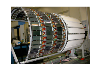
The modules are mounted onto light modular carbon-fiber substructures which also house the printed circuit boards for control electronics and for optical signal transmission from the detector to the surface electronics building. The light cooling pipes are an integral part of the supporting mechanics but not structural components. The modules are fixed to supporting blocks made from aluminum or composite material. The blocks are machined with a precision better than 20 m and are in direct dry contact with the cooling pipes. The final module mounting precision within a subsystem is expected to be better than 200 m. The integration of modules into the large substructures are under way as shown in Figure 1.
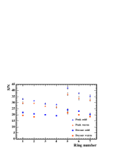
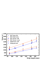
The performance of the substructures was measured in test beam experiments and system tests. In 2004 around 1% of all three subsystems were tested at CERN X5 with 120 GeV pions and GeV muons both at room temperature and at around C. We have experienced stable communication and readout, uniform noise distribution with small common mode noise. The signal/noise (S/N) ratio was found to be around 20 and the equivalent noise charge (ENC) consistent with expectations. The results testbeam are shown on Figure 2.
References
- (1) The CMS Collaboration, ”The Tracker Project, Technical Design Report”, CERN-LHCC 98-6; ”Addendum to the CMS Tracker TDR”, CERN-LHCC 2000-016.
- (2) F. Hartmann et al., ”Corrosion on Silicon Sensors”, to appear in Nucl. Instr. Meth. A, Vertex 2005 Conference Proceedings.
- (3) J.L. Agram et al., Nucl. Instr. Meth. A517, 77-93 (2004).
- (4) R. Bauer, K. Klein et al., ”Design and Test Beam Performance of Substructures of the CMS Tracker End Caps”, CMS NOTE 2005-025.