Cryogenic small-signal conversion with relaxation oscillations in Josephson junctions
Abstract
Broadband detection of small electronic signals from cryogenic devices, with the option of simple implementation for multiplexing, is often a highly desired, although non-trivial task. We investigate and demonstrate a small-signal analog-to-frequency conversion system based on relaxation oscillations in a single Josephson junction. Operation and stability conditions are derived, with special emphasis on noise analysis, showing the dominant noise sources to originate from fluctuation processes in the junction. At optimum conditions the circuit is found to deliver excellent noise performance over a broad dynamic range. Our simple models apply within the regime of classical Josephson junction and circuit dynamics, which we confirm by experimental results. A discussion on possible applications includes a measurement of the response to a cryogenic radiation detector.
I Introduction
Cryogenic devices are widely used in a broad range of applications like radiation detection, quantum cryptography, charge manipulation on the single-electron level, quantum Hall effect or in basic studies of mesoscopic transport. Measurement of the electronic properties of such devices usually requires sophisticated readout electronics. Detection schemes where the samples at cryogenic temperatures are remotely connected to room temperature electronics generally face the problem of reduced frequency bandwidth due to the impedance of long readout lines. In addition, the risk of noise pickup on the lines is intrinsically increased. Alternatively, signal readout relatively close to the sample can be accomplished with ‘Superconducting Quantum Interference Device’ (SQUID) amplifiers, which perform very successfully in many cases but require a delicate setup (shielding) and are usually constrained to commercially available systems. Amplification or impedance transformation on-chip or very close to the sample is also possible with a ‘High Electron-Mobility Transistor’ (HEMT), the dissipation of which may, however, quickly reach an unacceptable level.
In recent years it has been realized that probing the electronic transport in a cryogenic device with a radio-frequency (RF) signalSchoelkopf et al. (1998); Segall et al. (2002); Lu et al. (2003); Bylander et al. (2005); Day et al. (2003); Schmidt et al. (2005) may have considerable advantages compared to direct signal readout, mainly due to a substantial extension of the bandwidth. In those schemes the power of the reflected (or transmitted) RF signal from a properly tuned tank circuit is related to the electronic state of the device under test. The circuit needs to be carefully designed to minimize back-action on the cryogenic sample. Operation at microwave frequencies also naturally opens a potential way for frequency-domain multiplexing.Stevenson et al. (2002); Irwin and Lehnert (2004)
A promising readout scheme, which we present in this paper, consists of an on-chip analog-to-frequency converter, delivering a frequency signal of large amplitude which is easily demodulated with standard room temperature (phase-locked loop) electronics. It has the advantages of both the direct signal readout close to the sample and a large frequency bandwidth. Particularly, it is much easier to accurately analyze a frequency signal than to transmit a low-level analog signal through long readout lines and amplify it with room temperature equipment which typically shows inferior performance in terms of noise with increasing temperature. Our low-noise converter circuit is based on a hysteretic Josephson junction exhibiting relaxation oscillations. Related ideas using relaxation oscillations in Josephson junction were proposed for thermometryGerdt et al. (1979) or direct radiation detection,Nevirkovets (1998) both relying on the temperature dependence of quasiparticle population in the gap singularity peak of asymmetric junctions, and for the (double) relaxation oscillation SQUID,Mück et al. (1988); Gudoshnikov et al. (1989); Adelerhof et al. (1994) which is investigated and used as a magnetometer. In our case the circuit converts an analog current signal into a frequency with acceptable linearity over a broad operation bias and dynamic range.
In Sec. II we review the basic principle of a relaxation oscillation circuit and derive conditions for stable operation. Results from the model are illustrated with experimental data. A thorough noise analysis with implications for the circuit’s readout resolution is given in Sec. III. An optimized low-noise configuration with numerical estimates is considered in Sec. IV, followed by a discussion on possible applications in Sec. V. As an example we demonstrate the readout of a cryogenic radiation detector. The paper concludes with Sec. VI.
II Principle of operation
We assume a Josephson device with normal resistance , critical current , junction capacitance and superconducting energy gaps , where . It shall be connected in series with an inductance and both shunted with a resistor , as shown schematically in Fig. 1. The circuit is eventually current biased by a large resistor . A Josephson junction with a non-vanishing difference of the energy gaps shows a region of negative differential resistance in the current-voltage () characteristics. Voltage biasing the junction in that region, where acts as voltage source with , its operation is potentially unstable and the circuit can undergo relaxation oscillations.Albegova et al. (1969); Vernon and Pedersen (1968); Calander et al. (1982) A relaxation oscillation cycle, which is displayed in the diagram of Fig. 1, can be separated into four phases:

-
•
(A) Initially, when is turned on, the Josephson junction is essentially a short (supercurrent branch) and the current through increases with a time constant towards a value like until reaching within a time
(1) -
•
(B) Because the junction was current biased during phase (A) via a high-impedance it switches now to the quasiparticle branch by developing a voltage across until it is charged to . The inductance holds the current constant if is small enough, which means that in order to observe the “full swing” of the voltage oscillations, the inductive energy and the energy from the bias voltage must be sufficient to provide the charge on with , i.e. must be fulfilled. For the case of interest where this requirement is particularly true if
(2) Another requirement is undercritical damping of the circuit with . However, because , comparison with Eq. (2) shows that the undercritical damping condition is already implied by (2). The voltage switching time is on the order of which is negligibly short for satisfying (2).
-
•
(C) Similarly to phase (A) the current on the quasiparticle branch decays with (where is the corresponding resistance in that region of the characteristics including the shunt in series) from to like until reaching zero (or a local minimum close to zero) within time
(3) -
•
(D) The capacitor is discharged again to zero voltage according to the conditions in phase (B), but with a subtle difference regarding final locking to the zero-voltage state, as discussed in the noise section III.4.
Neglecting the short voltage switching times of phases (B) and (D), the relaxation oscillation period is given by . However, when biasing a Josephson junction at , the oscillation dynamics are dominated by the process in phase (A) with . Therefore, the relaxation oscillation frequency is essentially given by
| (4) |
where is the reduced bias current. A series expansion for yields
| (5) | |||||
| (6) |
These equations describe an almost linear analog-to-frequency converter. The same result follows from an expansion around , relevant for the readout of a variable resistance device in place of . The current-to-frequency conversion factor is
| (7) |
Figure 2 shows experimental relaxation oscillation data. The amplitude of corresponds to the gap voltage , and the dynamics follow the model predictions. In the operation range the effective oscillation frequency deviates from linearity by less than 10% (a larger operation range can also be chosen with an easy subsequent linearization of the results according to circuit calibration). Linear extrapolation of towards yields a frequency offset in agreement with Eq. (5).
Relaxation oscillations in Josephson junctions can be analyzed in terms of subharmonics of the Josephson frequency. This implies that the number of Josephson oscillations per relaxation oscillation cycle be much larger than unity in order to prevent significant harmonic phase locking of the two oscillating processes. That sets a constraint on the frequency response and we can write
| (8) |
and
| (9) |
where is the magnetic flux quantum. This argument is in line with the requirement
| (10) |
as stated in the literature.Whan et al. (1995)

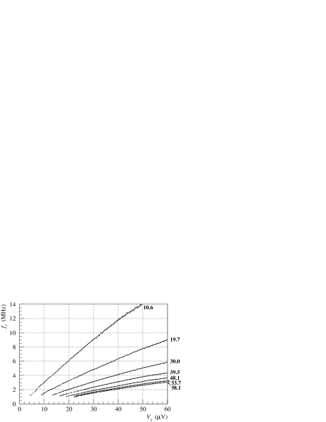
Modulation of by application of a magnetic field parallel to the Josephson junction results in a variation of the relaxation oscillation frequency according to Eq. (6). This offers a convenient way to tune the circuit’s dynamic properties as well as to extend the operation range to lower . Figure 3 shows measurements of as a function of for different . In order to take an modulation into account we denote as the factor by which the nominal value may be suppressed. In the limit and equal superconductors with gap the zero-field critical currentAmbegaokar and Baratoff (1963) is . Corrections due to small gap differences are safely neglected for our analysis and we can write
| (11) |
The dimensionless capacitance parameter , which is a measure for the damping strength of the junction, is given by
| (12) |
where is the Josephson plasma frequency. For a weakly damped and hysteretic Josephson junction we should choose larger than unity. The inequality (2) in terms of Eqs. (11,12) can be rewritten as
| (13) |
and substituting from (9) yields
| (14) |
This result is consistent with the condition as we required for Eqs. (8,9).
Finally, a comparison between (10) and (13) shows that the latter is the more stringent of both conditions by the factor . Consequently, the very minimum of is determined by relation (13), which constitutes, together with (14) and , the relevant conditions for proper observation of relaxation oscillations and which should help to choose appropriate circuit components.
III Noise and resolution
III.1 General
In this section we list the significant current noise sources referred to the circuit input (i.e. at ). Special attention is paid to experimental mean fluctuations of the relaxation oscillation periods, which are denoted by . Assuming an analog signal which requires a bandwidth in order to resolve its dynamics in time (i.e. a sampling time period ), we measure oscillations per sampled signal. The relative accuracy of a measurement improves with as
| (15) |
Because bias current fluctuations are linear to frequency fluctuations according to Eq. (7), we can also conclude in first order that . This yields an expression for the rms current noise of the signal sampled at :
| (16) |
Consequently, in the case of random and uncorrelated fluctuations we observe a white current noise spectrum with a density
| (17) |
apparently independent of . Because phase (A) of a relaxation cycle dominates the timing, we expect fluctuations in the critical current to be a major origin of noise.
III.2 Flicker noise in the critical current
The critical current of Josephson junctions can fluctuate due to stochastic charge trapping at defect sites in (or close to) the barrier, which are known as “two-level fluctuators”. A sufficiently large ensemble of such fluctuators generates a spectrum, with significant contribution only at low frequencies. According to empirical modelsVan Harlingen et al. (2004); Wellstood et al. (2004) the critical current noise density due to flicker noise can be described by
| (18) |
where is the junction area and is an average value obtained from collecting data over a wide range of different junction parameters.Van Harlingen et al. (2004) Scaling with was confirmedWellstood et al. (2004) for temperatures down to (although the authorsWellstood et al. (2004) found a higher noise level in their devices with ).
III.3 Critical current statistics from thermal activation
Escape from the zero-voltage state of a Josephson junction due to thermal activation is a well-known and widely studied phenomenon. It can be treated for a large variety of junction types and external conditions. For our noise analysis we can restrict ourselves to the simple “transition-state” modelKramers (1940); Hänggi et al. (1990) where a particle inside a well is thermally excited above the relative barrier potential and irreversibly leaves the bound state. This model is appropriate for underdamped Josephson junctions and is justified by typical device parameters and experimental conditions as given in the numerical examples (sections IV and V). Particularly, we assume intermediate operation temperatures satisfying
| (19) |
where denotes a Josephson coupling energy, sufficient to suppress the probability of retrapping from the running state,Kivioja et al. (2005); Männik et al. (2005); Krasnov et al. (2005) but at the same time not too low to prevent macroscopic quantum tunneling effects. According to the model there is a nonvanishing probability for transitions from the superconducting to the resistive state at current values . The lifetime of the zero-voltage state in a Josephson junction as a function of the reduced current can be expressed byLee (1971); Fulton and Dunkleberger (1974)
| (20) |
where is the “attempt frequency” of the particle in the well and is the relative potential height of the next barrier in the Josephson junction “washboard” potential. 111The argument in the exponent of Eq. (20) is in general notation with in first approximation, taking into account the crossover between classical and quantum limits. In the range of interest ( for ) the excitation is dominated by . The probability for the junction to have switched from the superconducting to the resistive state before time isFulton and Dunkleberger (1974)
| (21) |
By assuming small fluctuations compared to and using approximations in the limit , we can solve the integral by a similar approach to Ref. Kurkijärvi, 1972 which yields
| (22) |
The mean value of the observed critical current and its standard deviation are calculated in the Appendix and are found to be
| (23) |
and
| (24) |
where
| (25) |
Hence, is essentially a function of , with a weak dependence on . The approximations used for derivation of (23,24) are appropriate for . Similar results were obtained in Ref. Snigirev, 1983. The current noise density at the circuit input is, according to Eq. (17):
| (26) |
To verify our results and to compare with other modelsCarmeli and Nitzan (1983); Barone et al. (1985) of different formalism or treating different ranges of damping strength, we evaluated numerically the probabilities , the transition current distributions , and analyzed them with respect to shape, expectation value and width . We found that, within the range of allowed and reasonable model parameters, only the mean values differed quantitatively for different models, as should be expected for different initial conditions and excitation forms. However, there were insignificant differences in the distribution shapes and particularly of their widths . Therefore, Eq. 24 can be considered a good estimate for critical current fluctuations due to thermally activated escape, applicable over a wide range of .
III.4 Other noise sources
Thermal current noise from ohmic resistors is dominated by the shunt and corresponds to the standard Johnson noise . The voltage noise generated by and seen by the junction is, due to , not amplified and therefore equivalent to at the circuit input.
The real part of a good inductance vanishes. Therefore, can safely be considered as a “cold resistor” without thermal noise contribution. Pickup of external magnetic noise can be shielded and becomes negligible for small coils.
Because the Josephson current is a property of the ground state of the junction, it does not fluctuate. Hence, shot noise in Josephson junctions is only due to the quasiparticle current. The relaxation oscillations within our concept are dominantly determined by processes with the junction in the superconducting state. Therefore, shot noise by itself should be negligible in our case.
However, as a consequence of the random nature of the junction phases in the quasiparticle tunneling regime, the locking to the zero-voltage stateFulton (1971) at the end of an oscillation cycle occurs within a time spreadAdelerhof et al. (1994) on the order of . This results in an input current noise density
| (27) |
III.5 Noise conclusions
Combination of all noise sources derived above (and assumed to be uncorrelated) yields a total circuit input current noise density with . We make substitutions with respect to a notation of in terms of the primary circuit and operation parameters , , , , and :
| (28) |
where the constant coefficients are orthogonal to the other parameters. Dependence on junction area and capacitance in Eq. (28) is implicit by taking the products and to be constant in standard Josephson junctions, respectively, where is the specific (normal) barrier resistance, the barrier oxide dielectric constant and the barrier thickness. Furthermore, we have neglected the dependence in Eq. (24) assuming . Hence, we can minimize the total circuit noise with respect to the parameters in Eq. (28). In particular, appears to decrease with decreasing , (although satisfying ) and . However, a lower has to be compensated by a larger in order to satisfy Eq. (13), for the price of lower and a disadvantageous, although weak increase of noise in the second term of Eq. (28). Optimum values for and are found from a detailed balance of the noise contributions. Assuming, for instance, a negligible contribution from the fourth term in (28), a large value seems favorable. Due to , however, we see a conflict with a low noise requirement for the first term. This example implies a not too large ratio.
III.6 Dissipation and electron heating
Without formally relating dissipation processes to electronic noise, we consider local thermodynamics due to electron heating which may degrade the circuit’s performance. The main current through the circuit is dissipated in the shunt resistor resulting in a permanent power of . Successful removal of the excess energy is a matter of proper thermal anchoring (sufficiently large contact areas) to prevent overheating of . A similar power term arises during oscillations (in phases A and C) at the inductor . Both these dissipation terms essentially constitute simple heat loads to the cryostat. Their magnitudes are typically very small and the risk of local overheating of the lumped elements or excessive global heat overload is minor in standard cryogenic environments.
However, thermal nonequilibrium in the Josephson junction device may have significant consequences and deserves closer inspection. Relevant dissipation in the junction can be shown to occur in phase B with and in phase C with , where both are (referred to a full oscillation cycle) weighted with their corresponding time constants. Satisfying Eq. (2) yields , hence the heat in the junction is essentially . In order to remove the hot quasiparticles from the tunnel barrier region, normal metal trapping layers need to be attached adjacent to the superconducting junction electrodes. At very low temperatures the interaction between electronic and phonon subsystems in a normal metal vanishes, and the heat flow is described by , where is a material-dependent coupling constant,Wellstood et al. (1994) the volume of the normal metal and and are the temperatures of the electron and phonon system, respectively. The normal trapping layers will therefore experience an increased electron temperature . Subsequently, the energy stored in the normal “cooling fins” has to be transferred to the substrate. However, if the temperature difference is small and the “cooling fins” are made of thin films (i.e. large contact area to thickness ratio) the Kapitza resistance becomes negligibleWellstood et al. (1994) and one can safely assume to be equal to the cryostat temperature.
IV Numerical estimates
In order to build a relaxation oscillation circuit we are in principle free to choose any device or circuit component and derive the remaining parameters based on optimum arguments as discussed in the previous sections. As an example we start with a Josephson junction of given area , junction (superconducting) material and an operation temperature . The area determines with a typical in our standard devices and with for AlOx and . The choice of junction material is a choice of energy gaps , , determining , and . It is worth noting that, according to Eq. (28), a lower tends to result in a lower noise level. A lower is also preferable to exclude perturbations like Fiske modes from the gap region. However, since delivers the oscillation amplitude, a minimum level is required for proper resolution of the oscillating signal . This conflict can eventually be alleviated instead by a suppression of by the factor due to application of a magnetic field, increasing the oscillation frequency which may be a desired effect. Finally, with the choice of operation point , the required ratio and a minimum satisfying (13), the full properties of the circuit are determined.

Figure 4 shows a numerical example of a relaxation oscillation circuit as a function of junction size (side length ), assuming an Aluminum junction (), an operation temperature , the ratios , and , and an effective which is chosen 10 times larger than the minimum in (13). The results in Fig. 4 give an idea of the order of the parameter ranges, including the contributions from different noise sources. The flicker noise density (at ) was always at least times lower than any other noise contribution and is therefore not shown in this example. The invariant parameters of this configuration are: , , , , , , and .
It is apparent in Fig. 4 that fluctuations due to thermally activated zero-voltage escape (i.e. current noise ) are the dominant noise process in the range of small devices. For illustration the corresponding distribution functions of transition currents are included in Fig. 4. In spite of increasing distribution width with decreasing junction size , the noise density decreases due to a faster decay of .
| (fF) | (nA) | (nA) | (MHz) | (GHz) | (ps) | (ns) | 222These units refer to all four current noise density terms. | ||||||||||||
| 0.1 | 3.54 | 25.0 | 75.1 | 7.51 | 2.87 | 26.9 | 218 | 104.5 | 146.6 | 44.9 | 0.63 | 0.56 | 0.098 | 0.002333Value taken at . | 965 | 235 | 363 | ||
As a second numerical example we calculate a realistic minimum-noise circuit configuration without leaving the range of classical dynamics of Josephson junctions as assumed for our model. We choose an Al/AlOx/Al junction where we expect the best quality tunnel barriers and a sufficient oscillation output amplitude . The minimum junction size is restricted by the range of validity of our model, requiring and to prevent single-electron charging or macroscopic quantum tunneling effects, respectively.444The phase diffusion model in Ref. Kautz and Martinis, 1990 does not significantly alter the switching behavior (and thereby the noise) of our dynamical circuit even for moderate ratios, as long as is sufficiently large. This is just satisfied with a junction of area , which can be fabricated by standard -beam lithography. An operation temperature of is easily reached and maintained in modern cryostats even in the case of some moderately low dissipation in the circuit. The values for the circuit components follow from our definitions of , , , , and are listed in Table 1. The results show a total input current noise as low as about , with the dominant contribution from thermally activated zero-voltage escape. Flicker noise density at is at a negligible level and remains insignificant down to very low readout bandwidths . The total noise figure of this configuration is well competitive with the best commercial SQUID amplifiers. In addition, due to the advantage of improving noise behavior with increasing oscillation frequency, it delivers a bandwidth superior to most SQUID systems.
It is clear that the operation point for the current or voltage biased device under test is fixed to or in this example. For devices requiring different bias values (as in Ref. Furlan et al., 2006a) the circuit components have to be adapted with respect to the specifications.
As discussed in Sec. III.6 the total dissipated power in the circuit example above (Table 1) amounts to about . We assume the normal metal “cooling fins” attached to the junction electrodes to be thin films of thickness and with an area of . The effective electron temperature in these normal metal traps will then increase (from ) to about , which is absolutely acceptable with respect to power equilibration in the system as well as to the thermal properties and operation of the Josephson junction. Larger tunnel junctions will require proportionally enlarged “cooling fin” areas, which is feasible up to a practical size compared to the bulky dimensions of (and eventually ). Furthermore, if the normal metal traps also form the connecting leads, the trapping and cooling efficiencies may improve appreciably.
V Possible applications
We have developed the relaxation oscillation analog-to-frequency converter primarily for readout of cryogenic radiation detectors.Booth et al. (1996) The aim was to overcome problems or limitations in scaling to large number pixel readout. Besides the outstanding noise properties, a particularly nice feature of the relaxation oscillation circuit is its potential for simple implementation into a frequency-domain multiplexing scheme by tuning the oscillation frequencies of the individual analog-to-frequency converters to well separated values, and then using one single line to read them out. It should be taken into account, however, that a signal excursion from a detector generates a frequency shift, which should not overlap with a neighboring oscillator in the simplest case. A more sophisticated scheme could lock into the “dark” (no detector signal) characteristic frequencies and, upon disappearance of one channel due to an analog detector signal, remove the other frequency bands in order to recover the signal of interest.555In case of frequency band overlap, the signal, which is only partially recovered, can be reconstructed from a decent knowledge of the expected pulse shape. The circuit example in Table 1 is apparently not a good choice for a multiplexing readout due to fairly broad . However, if we accept a moderate increase in noise level by choosing larger junctions, fluctuations are easily reduced to (see Fig. 4). In that case, and taking into account that the circuits should all operate in a bias range , we estimate that up to about 10 oscillators can be implemented with sufficient separation. The different frequencies can be tuned by either different shunt resistors , different inductors or a careful variation of junction sizes (resulting in different ), whatever best meets experimental conditions and technical possibilities. One should also understand that combination of several circuit outputs by simple connection (e.g. through resistors, no amplification) reduces the amplitudes of the individual signals by a factor equal to the number of interconnecting channels. Required minimum signal-to-noise therefore limits the feasible number of multiplexed channels.
To test and demonstrate the working principle of a (single) relaxation oscillation circuit readout we have measured the response of a SINIS microcalorimeterFurlan et al. (2006b) to irradiation with X-rays. The detector which replaced was voltage biased. Figure 5 shows the results of an X-ray event. The circuit and device parameters were: , , junction size and effective critical current . The detector’s “dark” (or bias) current was , the measured analog signal peak current was , as shown in Fig. 5d. The relaxation oscillation frequencies from Fig. 5c, taken at the same operation point and conditions, were and , respectively. Taking into account the conversion factor , see Eq. (7), the analog and the frequency-modulated signal are perfectly compatible quantitatively as well as qualitatively (pulse shape). The noise level is about the same in both cases and is due to detector noise. The circuit noise alone is estimated to contribute about rms integrated over full bandwidth up to . We should say that the microcalorimeter device and circuit configuration are by no means optimal in this example, they are rather a preliminary choice of available components. Primarily, these results are of illustrative nature, demonstrating the principle and feasibility of cryogenic detector readout.

Other possible applications for relaxation oscillation based analog-to-frequency conversion can be, in a wider sense, considered for any type of cryogenic device operated at relatively low bias levels, exhibiting small variations of its electronic properties or actively delivering small analog signals. A list may include quantum dots and wires, single-electron devices and quantum Hall structures, to name a few. Due to the large bandwidth, the readout method is also attractive for detection of fast processes like quantum noise or background charge fluctuations. The resistors and in our scheme just represent a current and a voltage source, respectively, and can be replaced by the device of choice.
It is important to note, however, that the oscillator junction characteristics (essentially represented by ) may slightly vary from cooldown to cooldown and therefore cause a measurable spread in the conversion factor (7). Therefore, the circuit is unfortunately not appropriate for absolute measurements on a level as required e.g. by metrologists.
As a concluding experiment we propose a setup for high-precision thermometry at low temperatures, replacing the classical four-point measurement on thermistors. The temperature-sensitive element would typically replace to minimize dissipation. The difficulty of applying small analog excitations and detecting low output levels (across long wires), competing with noise, is circumvented by directly “digitizing” the small signal very close to the sensor with a low-noise converter. It is clear that this thermometer readout can only be operated in a limited temperature range (presumably one order of magnitude) where the junction dynamics (fluctuations, switching probabilities) are sufficiently insensitive to variations.
VI Conclusions
We have investigated the feasibility of a cryogenic low-noise analog-to-frequency converter with acceptable linearity over a broad range of circuit and operation parameters. The dynamical behavior can be well described by simple circuit theory and classical models of the single Josephson junction involved. Their agreement with experimental data is perfect. We have presented a thorough analysis of noise sources, where fluctuation processes in the Josephson junction appear to usually dominate the circuit’s noise figure for typical configurations and experimental conditions. The inherent broadband operation paired with very good noise performance offers a versatile system for a wide range of applications. As one possible example we have demonstrated the readout of a cryogenic microcalorimeter exposed to X-rays. Implementation into a multiplexing scheme was discussed and needs to be experimentally tested for a large channel-number readout.
Acknowledgements.
We are grateful to Eugenie Kirk for excellent device fabrication, to Philippe Lerch and Alex Zehnder for valuable and stimulating discussions, and to Fritz Burri for technical support.*
Appendix A
For the analysis of noise due to thermally activated zero-voltage escape an evaluation of the central moments of the probability density function is required, yielding expectation value and variance , where is given by Eq. (22) and subsequently denotes the standard deviation. Analytical integration can be circumvented, however, by approximating with a Gaussian distribution and solving for the appropriate values satisfying and , respectively. A general solution of is
| (29) |
where and is the Lambert function satisfying . An asymptotic expansion of for can be written as , where higher order terms are suppressed. Setting in Eq. (29) yields the expectation value
In the limit this expression approaches
| (30) |
Correspondingly, for we find an expansion
which, for , approaches
| (31) | |||||
If significantly deviates from unity the approximation
| (32) |
describes the relative distribution width of transition current fluctuations.
References
- Schoelkopf et al. (1998) R. J. Schoelkopf, P. Wahlgren, A. A. Kozhevnikov, P. Delsing, and D. E. Prober, Science 280, 1238 (1998).
- Segall et al. (2002) K. Segall, K. W. Lehnert, T. R. Stevenson, R. J. Schoelkopf, P. Wahlgren, A. Aassime, and P. Delsing, Appl. Phys. Lett. 81, 4859 (2002).
- Lu et al. (2003) W. Lu, Z. Ji, L. Pfeiffer, K. W. West, and A. J. Rimberg, Nature (London) 423, 422 (2003).
- Bylander et al. (2005) J. Bylander, T. Duty, and P. Delsing, Nature (London) 434, 361 (2005).
- Day et al. (2003) P. K. Day, H. G. LeDuc, B. A. Mazin, A. Vayonakis, and J. Zmuidzinas, Nature (London) 425, 817 (2003).
- Schmidt et al. (2005) D. R. Schmidt, K. W. Lehnert, A. M. Clark, W. D. Duncan, K. D. Irwin, N. Miller, and J. N. Ullom, Appl. Phys. Lett. 86, 053505 (2005).
- Stevenson et al. (2002) T. R. Stevenson, F. A. Pellerano, C. M. Stahle, K. Aidala, and R. J. Schoelkopf, Appl. Phys. Lett. 80, 3012 (2002).
- Irwin and Lehnert (2004) K. D. Irwin and K. W. Lehnert, Appl. Phys. Lett. 85, 2107 (2004).
- Gerdt et al. (1979) D. W. Gerdt, M. V. Moody, and J. L. Paterson, J. Appl. Phys. 50, 3542 (1979).
- Nevirkovets (1998) I. P. Nevirkovets, Supercond. Sci. Technol. 11, 711 (1998).
- Mück et al. (1988) M. Mück, H. Rogalla, and C. Heiden, Appl. Phys. A 47, 285 (1988).
- Gudoshnikov et al. (1989) S. A. Gudoshnikov, Yu. V. Maslennikov, V. K. Semenov, O. V. Snigirev, and A. V. Vasiliev, IEEE Trans. Magn. 25, 1178 (1989).
- Adelerhof et al. (1994) D. J. Adelerhof, H. Hijstad, J. Flokstra, and H. Rogalla, J. Appl. Phys. 76, 3875 (1994).
- Albegova et al. (1969) I. K. Albegova, B. I. Borodai, I. K. Yanson, and I. M. Dmitrenko, Zh. Tekh. Fiz. 39, 911 (1969), [Sov. Phys. Tech. Phys. 14, 681 (1969)].
- Vernon and Pedersen (1968) F. L. Vernon and R. J. Pedersen, J. Appl. Phys. 39, 2661 (1968).
- Calander et al. (1982) N. Calander, T. Claeson, and S. Rudner, Phys. Scr. 25, 837 (1982).
- Whan et al. (1995) C. B. Whan, C. J. Lobb, and M. G. Forrester, Appl. Phys. Lett. 77, 382 (1995).
- Ambegaokar and Baratoff (1963) V. Ambegaokar and A. Baratoff, Phys. Rev. Lett. 10, 486 (1963).
- Van Harlingen et al. (2004) D. J. Van Harlingen, T. L. Robertson, B. L. T. Plourde, P. A. Reichardt, T. A. Crane, and J. Clarke, Phys. Rev. B 70, 064517 (2004).
- Wellstood et al. (2004) F. C. Wellstood, C. Urbina, and J. Clarke, Appl. Phys. Lett. 85, 5296 (2004).
- Kramers (1940) H. A. Kramers, Physica 7, 284 (1940).
- Hänggi et al. (1990) P. Hänggi, P. Talkner, and M. Borkovec, Rev. Mod. Phys. 62, 251 (1990).
- Kivioja et al. (2005) J. M. Kivioja, T. E. Nieminen, J. Claudon, O. Buisson, F. W. J. Hekking, and J. P. Pekola, Phys. Rev. Lett. 94, 247002 (2005).
- Männik et al. (2005) J. Männik, S. Li, W. Qiu, W. Chen, V. Patel, S. Han, and J. E. Lukens, Phys. Rev. B 71, 220509 (2005).
- Krasnov et al. (2005) V. M. Krasnov, T. Bauch, S. Intiso, E. Hürfeld, T. Akazaki, H. Takayanagi, and P. Delsing, Phys. Rev. Lett. 95, 157002 (2005).
- Lee (1971) P. A. Lee, J. Appl. Phys. 42, 325 (1971).
- Fulton and Dunkleberger (1974) T. A. Fulton and L. N. Dunkleberger, Phys. Rev. B 9, 4760 (1974).
- Kurkijärvi (1972) J. Kurkijärvi, Phys. Rev. B 6, 832 (1972).
- Snigirev (1983) O. V. Snigirev, IEEE Trans. Magn. 19, 584 (1983).
- Carmeli and Nitzan (1983) B. Carmeli and A. Nitzan, Phys. Rev. Lett. 51, 233 (1983).
- Barone et al. (1985) A. Barone, R. Cristiano, and P. Silvestrini, J. Appl. Phys. 58, 3822 (1985).
- Fulton (1971) T. A. Fulton, Appl. Phys. Lett. 19, 311 (1971).
- Wellstood et al. (1994) F. C. Wellstood, C. Urbina, and J. Clarke, Phys. Rev. B 49, 5942 (1994).
- Furlan et al. (2006a) M. Furlan, E. Kirk, and A. Zehnder, Nucl. Instrum. Meth. A 559, 796 (2006a).
- Booth et al. (1996) N. E. Booth, B. Cabrera, and E. Fiorini, Annu. Rev. Nucl. Part. Sci. 46, 471 (1996).
- Furlan et al. (2006b) M. Furlan, E. Kirk, and A. Zehnder, Nucl. Instrum. Meth. A 559, 636 (2006b).
- Kautz and Martinis (1990) R. L. Kautz and J. M. Martinis, Phys. Rev. B 42, 9903 (1990).