The Large Analog Bandwidth Recorder and Digitizer with Ordered Readout (LABRADOR) ASIC
Abstract
Three generations of full-custom analog integrated circuits designed for low-power, high-speed sampling of Radio-Frequency (RF) transients in excess of the Nyquist minimum have been developed. These 0.25 CMOS devices are denoted the Large Analog Bandwidth Recorder and Digitizer with Ordered Readout (LABRADOR) ASICs and finally consist of 9 channels of 260 deep sampling. Continuous sampling is provided with common stop capability. Input analog bandwidth is approximately 1GHz and sampling speeds are adjustable from 0.02 to 3.7GSa/s. Completely parallel internal conversion supports 12-bit digitization and readout of all 2340 cells in under 50.
, , , and
1 Introduction
Observation of the early universe through neutrino messengers of the highest possible energies requires a detector of enormous instrumented volume. One promising means to observe such a large, radio-transparent target is viewing the Antarctic ice shelf via high altitude balloon [1]. Such a balloon-borne detector needs hundreds of high-speed sampling channels (multi-event buffering), operating over a frequency band from 200-1200 MHz [2]. Since all power must come from solar panels, and heat dissipation is a major problem, commercial flash ADCs were precluded.
For at least two decades a number of Switched Capacitor Array (SCA) devices have been reported in the high energy physics literature, for example [3, 4, 5], and many with sampling speeds high enough for greater than Nyquist sampling of a GHz analog bandwidth signal. These GSa/s devices have been used for low and high energy neutrino detection [6], particle physics [7, 8] and gamma-ray astronomy [9]. However, despite such high sampling speeds, all of these devices have analog bandwidth cutoffs which limit their use at UHF frequencies and above.
We present here the results of three generations of a high analog bandwidth ASIC designed to meet these instrumentation needs.
2 Architecture
A number of different CMOS SCA architectures have been discussed in the literature. An excellent summary of the storage circuit details and performance may be found in Ref. [10]. As will be seen below, in order to couple in high analog bandwidth it is necessary to limit the parasitic and storage capacitance of the SCA array. Thus a compact, minimal storage array was considered and initial prototyping looked promising [11]. This choice of a compact storage matrix was guided and synergistic with very similar storage architectures being explored for Monolithic Active Pixel Sensors (MAPS) [12] for charged particle tracking.
2.1 Theory of Operation
Employment of SCA techniques in CMOS processes have been effective in the areas of basic signal processing, continuous filter design, and programmable capacitor arrays, used for Digital-to-Analog (DAC) and Analog-to-Digital (ADC) conversion. As elements of a basic programmable filter, a simple inline capacitor between two switches may be used to form a frequency-controlled resistor, with resistance given by [13]:
| (1) |
for a given capacitor , being switched at frequency [Hz]. Almost arbitrarily complex filters, composed of these variable and configurations, can be formed and expressed in terms of poles and zeros in a transfer function, the mathematics of which is conveniently described via the -Transform [14], a staple of modern signal processing. As an example, from these simple building blocks, first order filters can be constructed as represented by the transfer function:
| (2) |
where , , , and is an overall normalization constant. Through choice of constants, one can form a Low-pass filter ():
| (3) |
or a High-pass filter ():
| (4) |
Since first-order filters only have one real pole, they cannot directly realize band-pass or notch filters. More flexible and universal are filters of second-order and beyond. Second order SC filters are often called biquad circuits and have may be expressed as
| (5) |
and is analogous to the continous time case where the transfer function may be represented by
| (6) |
where as long as the sampling frequency is much higher than the signals of interest, the approximation may be used. And from this point, standard pole-zero analysis can be used.
Beyond simple synthesis of rather complex filters using standard tools, the true power of this technique lies in pairing such SCA processing with operational amplifiers on an integrated circuit to achieve powerful sampling and signal manipulation capabilities. For instance, in analogy with an R-2R ladder topology, a multiplying DAC may be expressed using an array of switches and capacitors with the simple transfer function [15]
| (7) |
and ignoring the half-period delay indicated by the , can synethize an output voltage based upon a reference voltage via the expression
| (8) |
with the being the binary-coded digital signal, precisely as expected for a DAC. ADC topologies are now myriad and the focus of this paper is on a specific type - the transient waveform recorder. In some ways this makes use of the simplest SCA structure of them all, the Sample-and-Hold (S/H) circuit. The great power of the papers referenced above derives from the ever increasing speed and compactness of deep submicron CMOS processes.
While an idealized waveform recorder is simply an array of S/H circuits, parasitic capacitances require consideration of parasitic circuits like those referenced above. For the specific application at hand, parasitic inductances and capacitances are critical to storing analog waveforms with frequency content in the Giga-Hertz range.
2.2 Bandwidth Limitations
In order for an SCA storage device to be useful, it must have a decent number of storage cells. Load capacitance increases as a function of the number of switches connected to the incoming signal line, as well as the resistance-shielded storage capacitances when the switches are closed. For a properly coupled stripline into an ASIC, for a purely capacitive storage array, the 3dB roll-off is given as
| (9) |
Therefore, to obtain a 3dB bandwidth of 1.2GHz, the pure capacitance must be limited to approximately . This value is already smaller than that of the high-ESD protection diodes () provided in a standard design library used and therefore the input protection must be modified. A more accurate assessment of the input coupling performance requires a refined description of the input circuit model and will be discussed in much more architecture-specific detail below. In summary, to realize 1GHz of analog bandwidth with good coupling, will use the following design principles:
-
1.
stripline everywhere
-
2.
minimize input protection capacitance
-
3.
minimize switch drain, storage capacitance
Based upon these considerations, efforts have been made to maintain a coupling across the sampling array inside the ASIC. As a trade-off between storage depth and parasitic drain capacitance, 256 samples per input was chosen. Finally, the size of the storage capacitance was studied.
2.3 Storage Limitations
Limits are imposed on the minimum size possible for the storage capacitor. Since for a S/H circuit there is no means to perform a Correlated Double Sampling, an ambiguity in the actual stored value is given in terms of electron counting statistics by the usual expression
| (10) |
where is Boltzmann’s constant and temperure is in Kelvin. Matching the 12-bits of dynamic range of the sample storage conversion to a Wilkinson ramp voltage range of about 1V, a slope of approximately 0.25mV/least count is realized. At this level of sensitivity, the impact of the choice of storage capacitance value is seen in Fig. 1. At the upper left of this figure is a schematic representation of the basic storage cell for the first two generations of ASIC that utilized a transimpedance storage architecture. A reference value of is shown – about matching the least count of the ADC as shown.
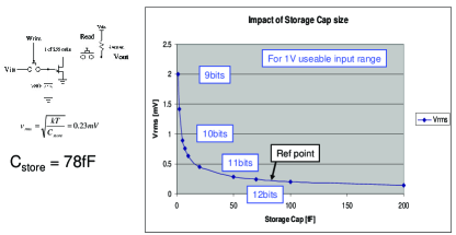
In the last generation a different readout is employed, although the same basic NMOS transistor gate capacitance storage is used. This constraint on minimum size is subsequently considered in the choice of storage capacitance. However reducing the storage capacitance too much makes switch charge injection and leakage current effects more prominent.
2.4 Architectural Details
Three generations of LABRADOR architecture ASIC have been designed, fabricated and tested. Their key features are summarized in Table 1. All have been fabricated in the TSMC m CMOS (LO) process and have been packaged in a 100-pin plastic TQFP package. Economics and package performance simulations [11] drove this decision. BGA packages were considered and may be used in the future to reduce the contribution due to lead inductance, however all test results are shown for this same 16.6 x 16.6 mm plastic package.
| Item | LAB1 | LAB2 | LAB3 |
|---|---|---|---|
| # of RF inputs | 8 | 8 | 9 |
| Samples/input | 256 | 256 | 260 |
| Total samples | 2048 | 2048 | 2340 |
| # of ADCs | 128 | 128 | 2340 |
| ADC Conversion cycles | 16 | 16 | 1 |
| Readout latency [s] | 2200 | 2200 | |
| Analog MUX out [s] | 25.6 | 25.6 | N/A |
| DC GND ref. | no | yes | no |
| Analog out | yes | yes | no |
| term. | end | end | input |
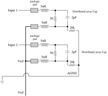
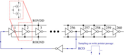
In contrast to the first two generations of LABRADOR ASIC, the third generation was a purely digital output device, changed input termination scheme to be at the input, and went to a massive array of Wilkinson ADCs (one per pixel). These differences and lessons learned will be highlighted below. The architecture of first two ASICs is illustrated schematically in Fig. 2. Examining Table 1, the primary difference between LAB1 and LAB2 was the attempt to provide a means to internally bias the RF inputs. This circuit did not work well due to high resistance noise coupling. LAB1 results are similar, though better in all cases. Eight RF input channels are each sampled by an array of 256 SCA storage cells. Sampling occurs continually until a trigger signal is generated.
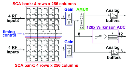
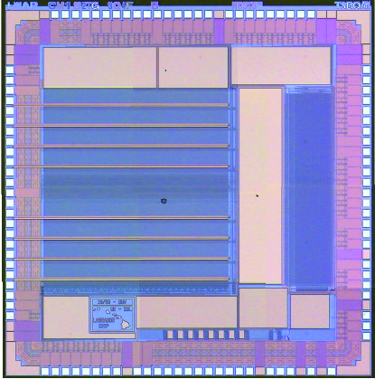
At this point the analog samples are held and not overwritten. These stored values are then selected and a transimpedance relay of the stored charge is made, which is either stored into input samples of an array of 128 channels of Wilkinson ADC or analog multiplexed and transferred off-chip for external ADC conversion. A die photograph of the approximately 10mm2 LAB1 device is shown in Fig. 3.
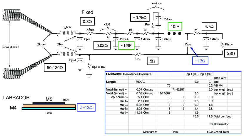
Layout of the LAB1 ASIC quite directly follows the arrangement of the functional blocks in the schematic diagram. While efforts were made to optimize the coupling of the input signal based on earlier efforts with the STRAW [11] architecture, the choice of LAB1 input structure represented a compromise, as shown in Fig. 4. Signals are straight input shots on the left and terminated in a resistor at the right. This choice is a trade-off between widening the signal trace, which would lower the microstrip impedance even below the shown, or having even larger resistive losses across the array. These resistive losses made for a vexing amplitude-dependence across the array. To address this issue in LAB3, a termination resistor is placed directly at the input to the detector. The termination resistor was removed from the array end. Since offset biasing could be performed directly at this input termination, the resistance of the signal line was unimportant and the on-chip stripline could be made exactly . Any reflection at the end of the array would be back-terminated, though this stub is short. At maximum signal frequency of 1.2GHz, for a stripline of 2mm long (about 10ps at ), the phase introduced by this stub is about
| (11) |
which is acceptable, though for operation at higher frequencies, such effects may be non-negligible. In all cases the input protection diodes have been completely removed. Current discharge is provided through a pull-down resistor to ground and voltage clamping is provided by external back-to-back RF diodes.
Other lessons gleaned from the first two LABRADOR generations included observing that while having analog samples available for external digitization has merits, non-linearities in the transimpedance response and temperature dependence were major issues. As space was available to permit completely parallel conversion of all 9 channels by 260 samples, in-situ conversion was adopted, as illustrated in Fig. 5. Including four extra “tail” samples avoids a sampling record gap during the interval in which the write pointer is returning to the beginning of the sampling window.
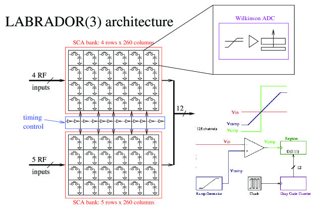
Details of the required timing and offset calibrations are discussed below. In order to accomodate the additional samples, as well as provide space for a Wilkinson comparator and 12-bit latch in each pixel storage cell, the die had to increase slightly to approximately 3.2 by 2.8 mm. Metal fill rules required covering the interesting parts of the die, making LAB3 far less photogenic than LAB1/LAB2 and thus not included. Addition of a 9th channel was done to allow insertion of a common reference clock into the data stream for each LABRADOR. This was found to be use for improving the temporal alignment of waveforms recorded by different chips.
All three generations use the same write pointer structure. This is a classical voltage-controlled inverter chain, with an odd number of stages such that a ripple continuously propages. An XOR circuit and a look-ahead signal are used to open each storage gate for the time it takes to transition from the look ahead to current locations (4-6 samples).
Despite best efforts at balancing the threshold voltage and NMOS versus PMOS L:W ratios, some amount of propagation variation is expected when the ripple edge across the array is transitioning low-to-high versus high-to-low, as shown below.
The ramping voltage for Wilkinson conversion is generated by
using a current source and either an internal or external reference
capacitor. In all testing shown below, an external 200pF capacitor is
used. An external () bias resistor sets the drive
strength of the current source to approximately A. A common
Gray-code counter is provided on chip and broadcast to all SCA cells.
When the ramp threshold is crossed in a particular cell, the current
count value is latched. Upon completion of ramping, all 2340 12-bit
values are available for random-access readout.
2.5 Design Evolution
In summary, the biggest changes in going from the LAB1/LAB2 architecture to the LAB3 are
-
1.
direct termination at array input
-
2.
Wilkinson conversion in each storage cell (no analog signal transfer)
-
3.
addition of a 9th (clock reference) channel
and by these choices good performance results have been obtained, as documented below.
3 Test Results
A variety of tests have been carried out to evaluate the performance of the LABRADOR series of waveform recorders. These measurements attempt to verify the degree to which the performance targets have been met, as well as characterize the system in preparation for UHF radio transient detection. Because of the superior performance of measured noise, bandwidth, linearity and digitization, results are shown the LAB3 ASIC.
3.1 Sampling Speed
The sampling speed dependence on an adjustable control voltage (ROVDD) is plotted in Fig. 6. Stable sampling speeds ranged from 0.02 to almost 4 GSa/s (limited by operation beyond the 2.5V nominal VDD rail voltage).
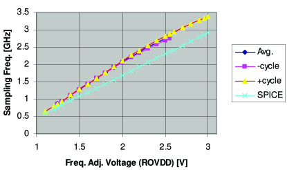
The SPICE simulation was fairly conservative and should be considered a lower-limit, pessimized for a worst-case spread in actual CMOS fabrication parameter values. While the sampling rate is defined as the cycle average of the so-called Ripple Carry Out (RCO), which is a copy of the write pointer monitored external to LAB3, the propagation speed of the high-to-low and low-to-high are seen to be different. At a nominal 2.6GSa/s this corresponds to about a 2% effect and is readily calibrated out by latching the RCO bit state at the time a trigger is recorded, as will be discussed later.
3.2 Input Coupling
Pulsing the input to the LAB3 chip with a fast risetime signal, a reflection is observed. Solving the usual expression
| (12) |
an impedance value of is determined. This is consistent with the measured DC resistance of the fabricated device, which appears to be about 20% higher than specified, though within spreads observed for silicide block in recent similar runs.
Because the signal of interest is an RF signal, a standard DC linearity scan performance is less important than evaluation with a realistic impulsive signal. Therefore, to determine the input coupling, linearity and cross-talk performance, an RF impulse was used as shown in Fig. 7. Most of the signal power of interest is in the steep high-to-low transition.
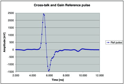
A 3GHz analog bandwidth oscillocope was used to record this reference signal. However the signal from the pulse generator itself was not flat in the frequency domain. Moreover this reference pulse has been bandwidth limited between 200-1200MHz, to match the frequency range of the ANITA instrument signal chain, in which these measurements have been performed.
Because determination of the analog bandwidth of the LAB3 device requires removing the intrinsic frequency of the RF pulse itself, its FFT has been measured and is displayed as the blue curve in Fig. 8. In red in this upper plot is the recorded LAB3 response.
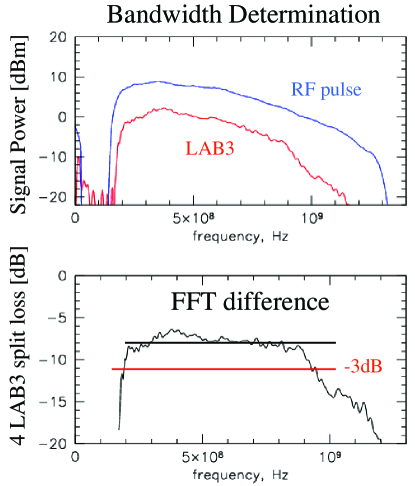
Taking the difference of these two curves, the analog response versus frequency is determined and shown in the bottom plot of Fig. 8. At the left edges of the curves the impact of the 200MHz high-pass band definition filters are seen. Of note is peaking of the signal in the 300-400MHz range, an effect seen in earlier testing. Taking the -3 dB point as the line shown, the roll-off frequency is just over 900 MHz, though signal power is still available out to 1200MHz. Four LAB3 are being tested in parallel and thus an ideal loss would be -6dB, indicating some amount of loss in the RF signal chain and coupling into the chip. Earlier tests on a dedicated, single LAB3 board, without band definition filters (e.g. 1200MHz low pass) indicated somewhat better higher frequency response and some of this loss may be due to components on the ANITA flight digitizer (SURF[2]) board used for evaluation. Therefore this curve may be considered a conservative lower bound on the analog bandwidth.
We note that the peaking observed is also present in the case of gaussian noise, though the peak of the distribution is a function of the input biasing network. This is likely due to resonant L-C response in the input front end and seems coupled to the cross-talk observed below.
3.3 Linearity
A determination of the linearity of the digitizing system has been made by varying the RF signal amplitude as displayed in Fig. 9.
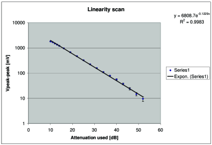
Since power attenuators are used, the response is characterized in dB and a linear fit is observed on a logarithmic plot. Good linearity is seen with just a hint of saturation at large signal amplitudes and some non-linearity at small signal amplitude due to the coaddition of board-level noise. Any non-linearity observed is likely due to non-linearities in the ramp generation circuit or comparator bias setting. Over a span of 40dB in dynamic range, the LAB3 output tracks input to within statistical measurement errors.
3.4 Crosstalk
By inserting the signal successively into the LAB3 channels, a cross-talk correlation plot was constructed as shown in Fig. 10.
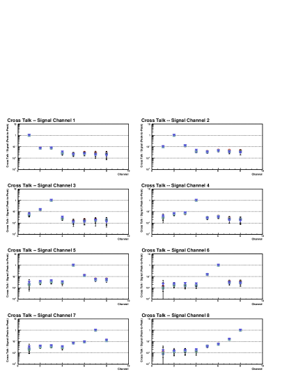
These values shown are determined by searching for a peak around the time of the input signal. Due to noise, statistically a few percent peak is measured even for the case of no cross-talk. Therefore the values shown are overestimated. For RF applications, even a 10% voltage crosstalk is only 1% in power.
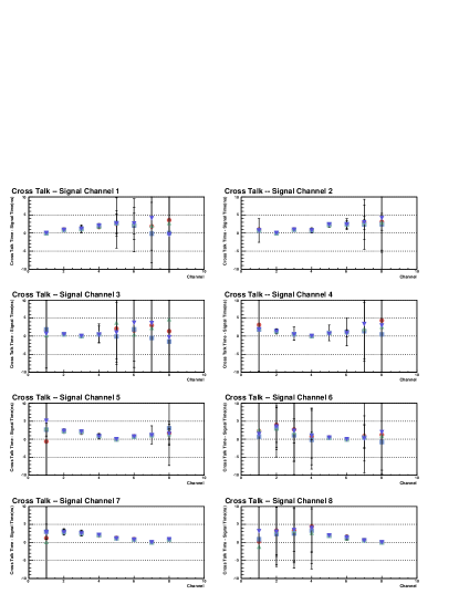
Nevertheless, for other applications it is important to understand the source of this effect. A hint to the origin of this crosstalk may be seen in Fig. 11.
Similar temporal and frequency dependence to the cross-talk can be reproduced in SPICE simulations, though the solutions are not unique. That is, the amplitude and phase information can be mimicked by tuning the voltage source output inductance of the pedestal network or with respect to bond-wire inductance stray coupling. Based on these results, a channel-dependent phase-lag to the cross-talk was predicted and subsequently verified qualitatively, as shown in Fig. 12.
In addition, a small component of direct radiative coupling between the on-chip striplines cannot be ruled out, though was difficult to model (metalic heat sinks would need to be taken properly into account in the 3D EM simulations). All results indicate that better packaging (lower inductance) and stripline shielding would help improve the observed effects.
4 Required Calibrations and Stability
In order to obtain the test results shown, a number of calibrations are needed. In the process of applying these, much improved resolution is obtained. Temperature dependence and timing precision limits are considered.
4.1 Gain and Pedestal Calibration
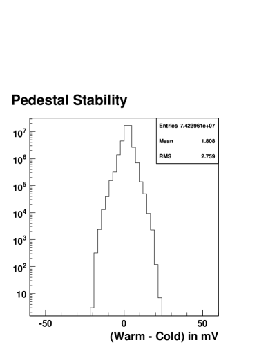
For the measurements shown, the gain has been adjusted to approximately mV/least count. A comprehensive pedestal histogram of all SCA storage channels (excluding channel 9) on the 36 LAB3 flown on ANITA is summarized in Fig. 13.
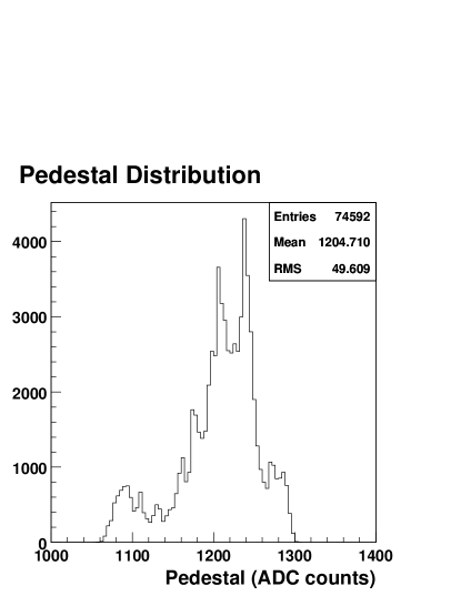
Channel 9 is excluded since it has a different voltage offset value due to the clock input biasing. The spread seen is a combination of 36 pedestal voltage differences, SCA-SCA variations, and Wilkinson ramp slope and starting voltage offsets. Also the gain of one LAB3 (values clustered around 1100) had an anamolously low gain. Overall the RMS of this distibution is just over 4%.
4.2 Timing Calibrations
In order to obtain the best possible timing resolution, a number of calibrations, due to the method in which the sampling is implemented, must be considered. As mentioned earlier, the write pointer is monitored using a copy of the signal called RCO. Since the sampling is done in so-called Common Stop mode, it is continuous until a trigger condition is formed. Thus all samples have already been recorded by the time a trigger is acted upon. In order for sampling to be continuous it is necessary for the write pointer to wrap around from the end of the array to the beginning, as illustrated in Fig. 14.
Four additional “tail” samples are provided to permit samples to be recorded during the time in which the write pointer is returning to the beginning of the array. Even though the physical distance is only 20-30ps at the speed of light, the need to go through an additional inverting stage (to form ring oscillator) and the capacitance associated with the long signal line back to the beginning of the array limit the speed of write pointer return.
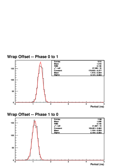
Also mentioned earlier, the write pointer speed of propagation across the array is a function of the transition direction. Likewise the delay time of write pointer return is also RCO phase dependent. The most general case of these calibration constants is illustrated in Fig. 15. From the measured RCO frequency (), the sampling frequency is determined as
| (13) |
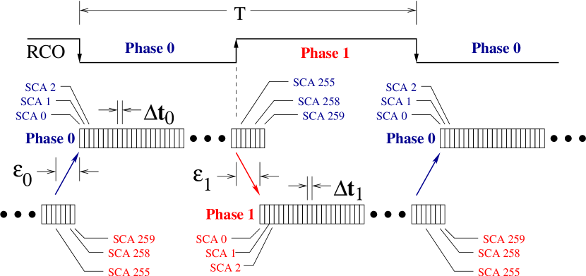
Expressing in terms of its period , half period corresponds to RCO phase 0 and half period corresponds to RCO phase 1, or
| (14) |
in which case the time step of an individual sample is expressed as
| (15) |
In general, as mentioned, the half periods and are not half the period :
| (16) |
which means that the average individual time steps in phase 0 () are different from those in phase 1 (). Likewise the delay time of the write point propagation for RCO () and for RCO are in general different and related to the difference between average and . Finally, due to transistor threshold dispersion, the actual widths of each of the time bins () can be slightly different.
Using a known periodic input signal, it is possible to generate calibration values for all of these parameters. An example of determination of the relative average and is shown in Fig. 16.
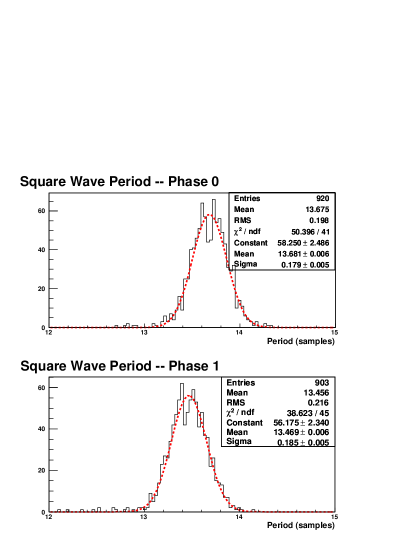
In each case the variable parameter is tuned until the spread or offset in the determined period is minimized. Because the period is well determined, the procedure is very efficient and requires a relatively small amount of calibration data.
Similarly, the write pointer wrap around delays, and , may be determined by constraining the measured period to be consistent across the write pointer wrap around. An example is shown in Fig. 17.
To a certain extent these calibration steps must be bootstrapped. For example, correctly minimizing the error on these parameters requires that the average time steps in each of the RCO phases be correctly determined. A subtlety here is that the RCO phase is recorded at the time a trigger signal (hold) is issued. Because the RCO latching in the data is not completely synchronous, there is in general a delay between the measured value of RCO and its actual value. This ambiguity is resolved by assigning a phase delay between the measured RCO that depends upon the address at which the hold was issued, the so-called “HitBus” value. The value of this delay is tuned in the data until the width of the measured period is again minimized.
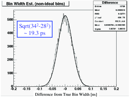
Finally, using a high frequency clock it is possible to constrain the average half period and assign its average value to the bin in which the positive/negative lobe peaks. Using this prescription the distribution histogrammed in Fig. 18 is obtained.
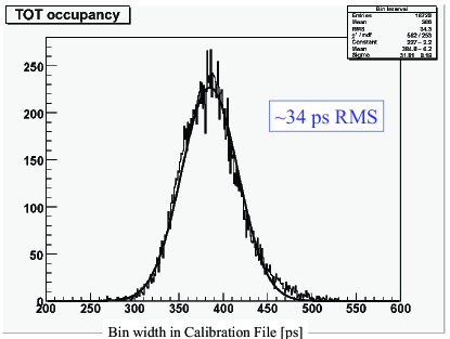
4.3 Time Resolution Limitations
Applying these timing corrections to the data leads to an improvement in the time resolution of signals in the data. The precise improvement depends upon the signal distance within the window (cumulative error) and method for correlating signal shapes to extract a timing feature for comparison.
To understand the intrisic performance limits and the significance of the bin-by-bin correction, a simple Monte Carlo study was performed to determine the extent to which the technique used to extract the observed timings would lead to the observed distribution. Introducing a completely random scatter (uniform distribution) of 15% to the nominal 386ps bin width, 600MHz sine MC was then synthesized and the algorithm applied. A value of 15% was determined empirically to provide a good representation of the observations in data. Due to irreducible errors in the specific implementation of this zero-crossing technique, application of these constants improves the timing resolution to about 28ps, as shown in Fig. 19. This has improved the resolution by about 20ps in quadrature, though perhaps there is still room for improvement. Since two edges are used to determine this time interval, the single edge measurement is about or about 20ps and probably is a limit with the current LAB3.
These determined parameters appear to be stable in time and only depend upon thermal effects, and described next.
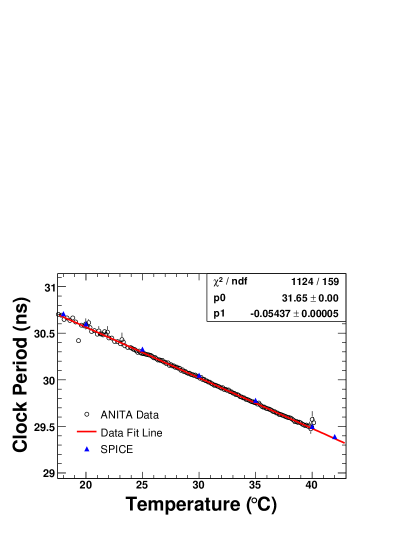
4.4 Temperature Dependence
The voltage controlled oscillator for the write pointer is fundamentally temperature dependent. During operation of LAB1 an external delay locking loop circuit was used to adjust ROVDD to compensate. However this circuit suffered from large phase noise as well as a nasty habit of locking onto a frequency subharmonic at power-on. Therefore, with the addition of a dedicated timing channel – needed to precisely align multiple LAB3 waveforms offline – ROVDD was fixed and timebase correction is implemented by fitting to the period of the reference clock.
The temperature dependence of the sampled frequency is shown in Fig. 20. Good agreement is seen with SPICE simulations of the temperature dependence, once an operating reference point is set. This fine tuning is needed to correct for the overly pessimistic parasitic capacitance estimate used earlier in simulating the ripple oscillator frequency. Using the reference clock signal on channel 9, this temperature dependence of the VCO is corrected in the offline analysis. A fit to this dependence gives a change of approximately 55ps/∘C over the 30ns period of the 33MHz reference clock, or about 0.2%/∘C.
In contrast, the pedestals are a very weak function of temperature. In Fig. 21 is displayed the difference in pedestal values taken after an ambient temperature change of approximately 17∘C.
Taking this difference, an estimate of the pedestal temperature dependence is
| (17) |
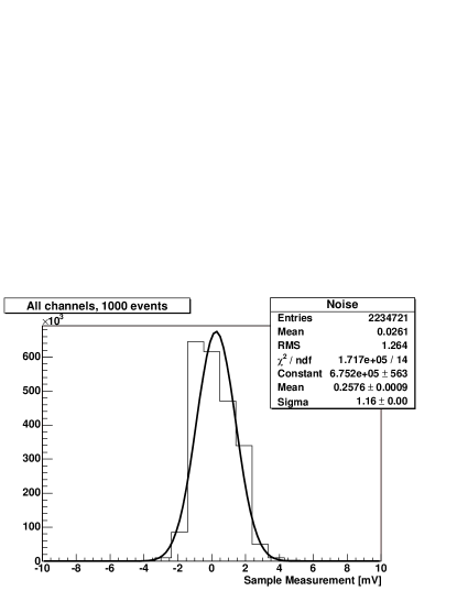
For reference, and to illustrate the typical chip-level noise, an example noise run is shown in Fig. 22. Representative noise values are about , though there is some non-gaussian behavior in the combined distribution of 2.2 million samples from 9 separate RF channels.
4.5 Interleaved Sampling
Right at Nyquist sampling of UHF RF sine wave signals visually appears undersampled to most observers. This is due to expectations from seeing smooth curves generated by 20+ GHz offset interleaved sampling of a repetitive waveform, provided by most digital signal oscilloscopes. By providing precise external delays it is possible to enhance the sampling speed and provide oversampling with the LAB3 chip. Interleaving of 8 inputs, running at 2.5GSa/s each has been done to provide single-shot recording of a 400MHz sine wave signal at 20GSa/s, as shown in Fig. 23. Each color represents the samples recorded by a single channel.
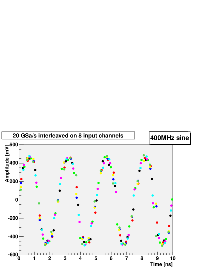
While there is some scatter due to the delays not being perfectly tuned, this indicates that there is still more performance to be gained by increasing the analog bandwidth yet further and implementing such interleaving. For low power and very high sampling rate applications, where signals may not be repetitive, this technique may be useful. This and other improvements are considered next.
5 Future Directions
Beyond increasing analog bandwidth, to fully exploit the enhanced sampling speed of deep submicron processes, there is a desire to increase sampling depth. This is being explored in a follow-on device designated the Buffered LABRADOR (BLAB) ASIC. While the sampling speed increases below 0.25m, loss of dynamic range due to reduced rail voltages and increased leakage current may preclude going to smaller feature sizes.
6 Applications
During December 2006 to January 2007, 36 LAB3 ASICs flew successfully at 120,000 feet for 35 days around the Antarctic continent. Some of the test results shown above are from this data set. During this same period, test deployments for an in-ice radio detector, using this device, were made at the south pole in conjunction with the IceCube array [16]. Recently, these ASICs were evaluated in a collidering beam environment for upgrade of the Belle Time-Of-Flight readout [17], and a variant for operation at a Super B-factory [18] is being developed for high timing precision, single photon recording [19]. For these future applications, a deeper sampling depth is highly desirable and such a device is currently being prototyped.
7 Summary
A Switched Capacitor Array (SCA) device has been developed in a 0.25m CMOS process with a 3dB analog bandwidth of almost a Giga-Hertz, capable of being sampled at many GSa/s, or well above Nyquist minimum. Sampling is performed at low power and the entire array of 9 channels by 260 samples can be digitized to 12-bits of resolution and read out within 50s. With calibration excellent time and sample voltage resolution have been obtained over a large range of temperature and sampling speeds.
8 Acknowledgements
This work was supported by the National Aeronautics and Space Administration (ROSS Program), the Department of Energy (HEP Division) University of Hawaii base program support as well as support from the Advanced Detector Research program.
References
- [1] P.W. Gorham et al. (ANITA Collaboration), Submitted to Phys. Rev. Lett., hep-ex/0611008, SLAC-PUB-12286.
- [2] G.S. Varner et al. (ANITA Collaboration), Detection of Ultra High Energy Neutrinos via Coherent Radio Emission, Proceedings of International Symposium on Detector Development for Particle, Astroparticle and Synchrotron Radiation Experiments (SNIC 2006) pp 0046, SLAC-PUB-11872.
- [3] S. Kleinfelder, IEEE Trans. Nucl. Sci.35 (1988) 151; IEEE Trans. Nucl. Sci.37 (1990) 1230.
- [4] K.L. Lee et al., IEEE Trans. Nucl. Sci.38: 344-347, 1991.
- [5] G.M. Haller and B.A. Wooley, IEEE J. Solid State Circuits 29 (1994) 500; IEEE Trans. Nucl. Sci. 41 (1994) 1203.
- [6] S. Kleinfelder, IEEE Trans. Nucl. Sci. 50 (2003) 955.
- [7] C. Brönnimann, R. Horisberger and R. Schnyder, Nucl. Instr. Meth. A420 (1999) 264.
- [8] S. Ritt, Nucl. Instr. Meth. A518 (2004) 470.
- [9] E. Delagnes et al., Nucl. Instr. Meth. A567 (2006) 21.
- [10] S. Panebianco et al., Nucl. Instr. Meth. A434 (1999) 424.
- [11] G.S. Varner et al., Monolithic Multi-channel GSa/s Transient Waveform Recorder for Measuring Radio Emissions from High Energy Particle Cascades, Proc. SPIE Int.Soc.Opt.Eng. 4858 (2003) 31.
- [12] G. Varner et al., Nucl. Instr. Meth. A541 (2005) 166; Nucl. Instr. Meth. A565 (2006) 126.
- [13] P. Allen and E. Sanchez-Sinencio, Switched Capacitor Circuits, Van Nostrand Reinhold, 1984.
- [14] R. Unbehauen and A. Cichocki, MOS Switched-Capacitor and Continuous-Time Integrated Circuits and Systems, Springer-Verlag, 1989.
- [15] R. Gregorian and G. Temes, Analog MOS Integrated Circuits for Signal Processing, John Wiley & Sons, Inc., 1986.
- [16] H. Landsman, A. Karle et al. (IceCube Collaboration) and G. Varner and L. Ruckman, to be published International Cosmic Ray Conference 2007 proceedings.
- [17] J. Rorie and G. Varner, Signal Timing and Readout (STaR) pipelined upgrade for the Belle TOF System, to appear Proceedings of the 2007 IEEE Nuclear Science Symposium.
- [18] S. Hashimoto (ed.) et al., KEK-Report-2004-4 (2004).
- [19] L. Ruckman and G. Varner, Photodetector Readout Monolithic with Precision Timing, to appear Proceedings of the 2007 IEEE Nuclear Science Symposium.