2005 International Linear Collider Workshop - Stanford,
U.S.A.
Monolithic CMOS Pixel R&D
for the ILC at LBNL
Abstract
An R&D program on monolithic CMOS pixel sensors for application at the ILC has been started at LBNL. This program profits of significant synergies with other R&D activities on CMOS pixel sensors. The project activities after the first semester of the R&D program are reviewed.
I INTRODUCTION
The anticipated ILC physics program requires pixel sensors with performances well beyond those obtained for the experiments at LHC in terms of single point resolution and material budget. At the same time the ILC experimental environment, with its lower event rate and radiation flux, admits Si sensors that are substantially thinner, more precise and more segmented than at the LHC and thus motivates new directions for R&D to achieve these performance ilc . LBNL has played a major role in Si detector development and it is currently engaged in a number of related projects, including the ATLAS pixel project, thick CCD development for SNAP, CMOS pixel R&D for the STAR upgrade and also CPCCDs and CMOS pixels for application at synchrotron light sources and electron microscopy. Monolithic CMOS pixel sensors offer several desirable features for application in collider experiments. The STAR experiment at RHIC has engaged in the first vertex detector based on CMOS pixels, under the guidance of the STAR group at LBNL. The ILC R&D program aims at addressing key R&D issues, building on the significant know how established at LBNL, and exploiting synergies and opportunities at the interface between these different fields of applications.
The R&D program on CMOS pixel sensors for the ILC started in Fall 2004 and it is addressing three main issues: the characterization of pixel sensors and the simulation of their response in the ILC physics and background environment, the test and characterization of thinned pixel sensors and the design and testing of new pixel test structures embedding on chip data reduction capabilities to specifications set by the ILC requirements. This paper reviews the project activities after the first semester of the R&D program.
II SENSOR CHARACTERIZATION
In order to perform tests of charge collection a setup based on an highly collimated light beam has been developed. The system uses a set of LED and laser diodes of different wavelengths, in the range 850 nm 1300 nm, pigtailed to a single-mode Corning HI1060 optical fiber with a 6 m core diameter and a numerical aperture of 0.14. The light is focused through an achromatic doublet lens, with 5 mm focal length, onto the detector surface. The choice of laser wavelength allows to probe the charge collection mechanism from a penetration depth of 15 m to the full wafer thickness. The system is mounted on a pneumatic isolation workstation to reduce the effect of vibrations. The light beam position on the detector plane and the focal distance is controlled by a computer-controlled stage with sub-m resolution.
The laser diode can be operated both in DC and in pulsed mode. Laser pulses are generated by modulating a DC current source with a fast pulse through a bias-tee (Picosecond Pulse Lab Model 5550B). The drive pulse is generated by a Picosecond Pulse Lab pulser (Model 2600) and allows pulse lengths in the range 0.5-100 ns which can be triggered from the FPGA controlling the chip readout, thus ensuring its synchronization with the detector readout cycle. In order to reduce the sensor noise, measurements can be conducted in a test chamber able to reach .
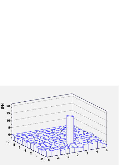
The set-up has been tested using several MIMOSA-5 chips mimosa . Light can be focused to a spot smaller than the pitch size of 17 m, such that the induced signal appears on a single pixel (see Figure 1). In these conditions, extensive scans can be performed to determine the cluster size and the charge collection properties as a function of the position of the light spot to the reference pixel.
In the test set-up the detector is mounted on a mezzanine card, specific to the chip design, connected to a readout board. This includes a Xilinx FPGA for controlling the readout sequence and 12-bit ADCs. Data is transferred from the board to the DAQ PC through a National Instruments I/O card. Data reduction can be performed online within a LabView program. This program controls also the stage position, the laser and the chip bias voltage and current. It computes pedestals and noise, in absence of signal, and performs correlated double sampling (CDS) and pedestal subtraction. The data is then transformed into the LCIO format, which is the standard as persistency model for ILC data, and written to disk for the subsequent offline analysis. A C++ program performs pedestal and noise initialization, if not already done on-line, updates their values through the run and produces tuples for further analysis and cluster visualization in ROOT. Chip pedestal, noise and dead or noisy pixels can also be stored in a condition database and retrieved for analysis. The use of a standard LCIO format, allows the same clustering and reconstruction software to be applied to both real lab test data and events simulated using GEANT 4.
III SENSOR BACK-THINNING
Sensor thickness is a major issue in the design of the ILC Vertex Tracker. The requirement to obtain a multiple scattering term as low as (m/GeV) in the track extrapolation accuracy, for a multi-layered detector, pushes on the sensor thickness. Further, the amount of material located in front of the calorimeter needs to be minimized to allow for optimal energy flow performance. CMOS pixel sensors, with their active epitaxial layer of only few m to m, can be back-thinned without losing, in principle, any significant fraction of the collected signal. However, there are several factors which need to be verified. Signal losses may arise both from disturbances to the charge collection mechanism introduced by the back-thinning process as well as by the loss of charge carriers created in the bulk. Several MIMOSA-5 chips have already been back-thinned to 50 m aptek , tested with a source and found to function. The thinning has been performed on diced chips with an yield of 94% and a thickness constant to better than 5 m. In order to carefully assess the effects of the back-thinning process on the charge collection mechanism, a new set of tests is presently being conducted. They aim at a full characterization of the same pixel sensors, both before and after back-thinning, for various thickness values. A set of six MIMOSA-5 chips are being used for these tests. The test procedures includes the characterization of the chip response to laser light of different wavelengths and to a collimated X-ray source. The procedure being adopted is as follows. Detectors are first mounted on a bare mezzanine card using WaferGrip dissolvable thin film adhesive and wire-bonded. Afterward the detector chip is masked and the mezzanine card is loaded with its components. After having been fully characterized in the test setup described above, the detector is removed and sent for back-thinning aptek . The thinned detector is then glued back on the mezzanine card and wire bonded. This procedure has already been successfully tested. The back-grinding process is able to accommodate for the small residue of bond wire left on the bonding pads and deliver the chips ground to the correct thickness and with parallel sides. We begin by characterizing the detector gain by calibrating to the 5.9 keV peak. Since the gain depends on the reference voltage supplied to each of the 4 sectors of the detector this also allows to optimize the voltage setting. The study of the charge collected for the 5.9 keV X-rays converting under a single pixel, will provide a first characterization of the charge collection properties of the sensors before and after thinning. The detector response to the collimated laser spot, will allow to compare the charge collection process for charge carriers produced at different depths, depending on the laser wavelength.
IV CHIP DESIGN
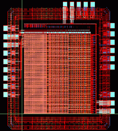
We are leveraging developments in other areas in order to support vertex detector R&D for the ILC. As a first step, we have made a small active pixel test chip in the AMS 0.35 m OPTO process. Processes specifically for CMOS imagers (so-called OPTO) are excellent candidates for particle detection applications, as they have thicker epitaxial regions, and thus better signal to noise performance, and much lower leakage current compared to conventional digital processes. The circuit consists of arrays of 3-transistor active pixels. An identical 3T layout is repeated at 10, 20 and 40 m pitch in order to study charge collection properties and optimize the pixel size (see Figure 2). Five analog outputs are provided, and the column multiplexers are arranged so that five adjacent pixels are output at the same time. Testing of the chip will be carried out in Fall 2005.
Although this first test circuit has only analog outputs, a device for the ILC should have on-chip digitization. We have begun to study ADC options. One possibility is to use a per-column Wilkinson architecture. Active pixel sensors in 0.25 m CMOS have already been developed at LBNL, for a different application, with 10-bit Wilkinson ADCs on a 19 m pitch. Although the Wilkinson architecture is attractive, as it is simple and has a low power dissipation, speed capabilities are marginal for the ILC application. Therefore we are presently considering a pipelined approach for a pixel architecture with analog CDS. An N-bit pipelined ADC can, in principle, be constructed from N cells consisting of a 1-bit ADC, a 1-bit DAC and a gain 2 amplifier. As the operation is pipelined, each stage can make use of the full digitizing time, i.e. a 4-bit pipelined ADC running at 50 MHz would provide a digital output every 20 ns, with a 60 ns latency and each cell would use the full 20 ns for the 1-bit operation. The 1-bit approach fails when offsets are taken into account, so 1.5-bit ADCs and DACs are used. As precision requirements are reduced, the pipelined approach improves in speed, power consumption and size, so that a 4-5 bit pipelined ADC on a 20 m pitch at 1 mW/channel should be feasible.
Acknowledgements.
This work was supported by the Director, Office of Science, of the U.S. Department of Energy under Contract No. DE-AC02-05CH11231. This research used resources of the National Energy Research Scientific Computing Center, which is supported by the Office of Science of the U.S. Department of Energy under Contract No. DE-AC03-76SF00098. This activity is carried out in collaboration with IReS, Strasbourg (France). We wish to thank Marc Winter for sharing with us precious know how and providing several chips developed by his group. We are also grateful to Howard Matis and Michelle Tuchscher for their help.References
- (1) M. Battaglia, Nucl. Instr. and Meth. A 530 (2004), 33.
- (2) Yu. Gornushkin et al., Nucl. Instr. and Meth. A 513 (2003), 291.
- (3) The back-thinning is a commercial process done at Aptek Industries, Inc., San Jose, CA (http://www.aptekindustries.com/).