Performance of the CMS Pixel Detector at an upgraded LHC
Abstract
The CMS experiment will include a pixel detector for pattern recognition and vertexing. It will consist of three barrel layers and two endcaps on each side, providing three space-points up to a pseudorapidity of 2.1. Taking into account the expected limitations of its performance in the LHC environment an 8-9 layer pixel detector for an upgraded LHC is discussed.
Key words: LHC, super LHC, CMS, tracking, pixel, silicon, radiation hardness
, , and ††thanks: Corresponding author; e-mail: Tilman.Rohe@cern.ch
1 Introduction
The tracker of the CMS experiment consistes on silicon detectors only. The region with a distance to the beam pipe between 22 and 115 cm is equipped with 10 layers of single sided silicon strip detectors covering an area of almost 200 m2 with about readout channels (strips)[1, 2]. The smaller radii will be equipped with a 1-m2-pixel detector containing about readout channels (pixels) providing three precision space points up to a pseudorapidity of 2.1 [1]. These unambiguous space points allow an effective pattern recognition in the multiple track environment close to the LHC interaction point. Further the precision of the measurement is used to identify displaced vertices for the tagging of b-jets and -leptons.
In its final configuration the pixel detector will consist of three barrel layers and two end disks at each side. The barrels will be 53 cm long and placed at radii of 4.4 cm, 7.3 cm, and 10.2 cm. They cover an area of about with roughly 800 modules. The end disks are located at a mean distance from the interaction point of 34.5 cm and 46.5 cm. The area of the 96 turbine blade shaped modules in the disks sums up to about .
To achieve the necessary spatial resolution, analogue interpolation between neighbouring channels will be performed. The 4-T-strong magnetic field in the CMS inner detector causes a Lorentz angle of up to (unirradiated detector at 100 V bias voltage) [3] and distributes the signal over several pixels. For this reason the pixel size of was chosen.
The two main challenges for the design of the pixel detector are the high track rate and the high level of radiation. The former concerns the architecture of the readout electronics. For the 4 cm layer it has to locally store the hit information of about tracks per second and cm2 at full LHC luminosity () for the latency of the 1st level trigger (s). The high radiation level mainly affects the charge collection properties of the sensor, which degrades steadily. In order to preserve a spatial resolution of better than m, which is required for efficient b-tagging, the pixel modules will be replaced after a fluence of .
A possible luminosity upgrade of LHC is currently being discussed. With a minor hardware upgrade a luminosity of cm-2s-1 might be reached. Later major investments will aim for a luminosity of cm-2s-1 [4]. Already the first stage of the accelerator upgrade will require a major upgrade of the tracker. The granularity of the strip detectors will become insufficient and these detectors will have to be replaced by pixel devices up to a radius of about 60 cm. As the area to be covered by such a system is in the order of 10 m2, the choice of the detector concept will be governed by financial considerations. Ideas for such cost effective pixel detectors are given in section 3 and 4.
The inner regions of the tracker will have to face an unprecedented track rate and radiation level as shown in Fig. 1.
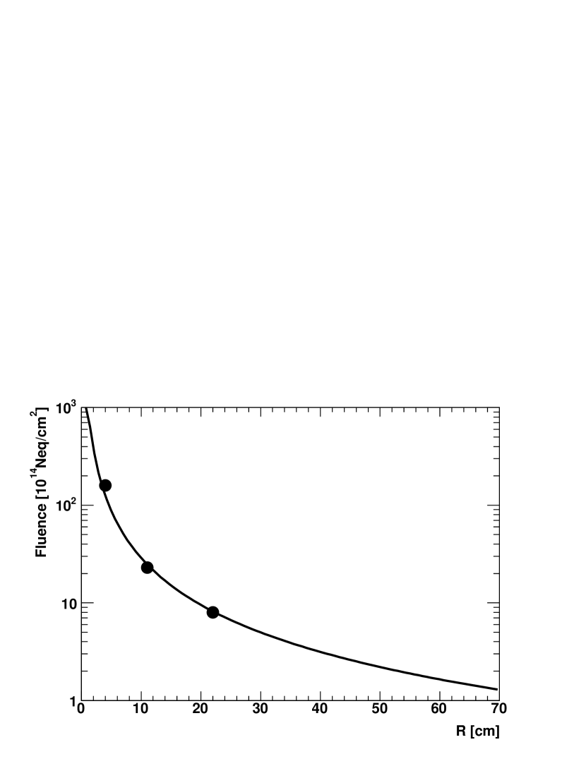
The detectors placed at a radius of 4 cm have to withstand the presently unreached particle fluence of or must be replaced frequently. The operation limit of a present type hybrid pixel system is discussed in section 2. This is used as a starting point for a proposal of an 8-9 layer pixel system for an upgraded CMS pixel tracker.
2 Limitations of a present-Type Pixel Detector at an upgraded LHC
The limiting factors for the operation of a hybrid pixel system at an upgraded LHC remain the same as for the design of the initial CMS pixel detector: the track rate for the readout electronics and the radiation induced degradation for the sensors.
2.1 Sensor
Since the late 1980’s the radiation induced degradation of silicon detectors has been systematically studied. The main effects are the increase of the leakage current, trapping and the space charge. While the space charge increase is reduced for silicon containing a high concentration of oxygen [5], no dependence on the starting material could be found for the other two parameters. Assuming that the increased leakage current can be controlled by cooling, the reduction of the signal by charge trapping presently sets the ultimate limit of the use of silicon detectors.
Trapping of the signal charge is caused by irradiation induced energy levels in the band gap. It can be described by the trapping time which is inversely proportional to particle fluence.
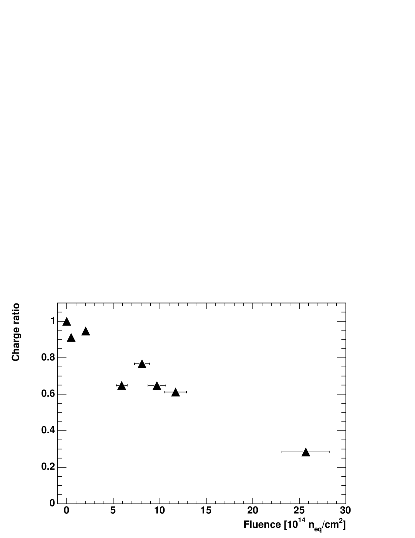
This is illustrated in Fig. 2 were the signal degradation in a m thick pixel detector with increasing particle fluence is shown. In this measurement the bias voltage was adjusted for each fluence to values between 100 V and 600 V [6]. A further increase will not increase the signal level considerably. Up to a fluence of a total signal above 12 000 electrons originating from the whole detector thickness [3] is achieved which is sufficient for an efficient particle detection at comparator thresholds of 2000-3000 electrons.
At higher fluences the signal steadily decreases further. It is not straightforward to decide which signal level will be sufficient for efficient tracking. If it is possible to operate with a signal of 6000 electrons, a fluence of will be reachable. Tests with pixel detectors irradiated to this level have been performed and show encouraging results [6]. This corresponds to the radiation level at a radius of 8 cm, leaving only the radiation hardness of the innermost (4 cm) layer unsolved. Strategies to reach the level of radiation hardness required there are the subject of the CERN-RD50 collaboration [7]. When a pixel detector is operated at such a high fluence, charge sharing will be much reduced due to the decreasing Lorentz angle and the diminished range of signal collection depth. This will eventually limit the spatial resolution to the binary resolution of pitch/. If the value of better than m has to be achieved also at fluences above , the pixel pitch has to be reduced which requires a redesign of the readout chip. In this case it has also to be reconsidered, whether the analogue signal processing performed by the present CMS pixel readout chip is still useful.
2.2 Readout Chip
The radiation hardness of ASICs fabricated in m technology seems to be sufficient up to ionisation doses111The tolerance against charged particles at this high level has still to be checked. A reduction of the charge carrier mobility might lead to speed limitations and the increase of the junction leakage current could discharge dynamic nodes and lead to an increased standby power. exceeding 250 kGy. The performance of the readout chip is therefore limited by the readout losses due to the high rate of tracks. As one would like to avoid a complete redesign of the present CMS pixel chip, the limits of its architecture will be discussed in section 2.2.2, after the main mechanisms for data loss has been explained in the next paragraph.
2.2.1 Architecture and Readout Losses of the CMS Pixel Readout Chip
The architecture of the readout chip was adjusted to the environment of the LHC and is described in detail in [8]. Here only the features necessary to understand the inefficiency mechanisms are discussed.
Each pixel contains a preamplifier, shaper and comparator. When the amplitude of the shaper exceeds the comparator threshold, the periphery of the chip, which is shared by two columns of pixels, is notified and the amplitude is stored in a sample-and-hold capacitor. The double column periphery then creates a time stamp and initiates a scan (“column drain”) which copies the amplitude of all hit pixels into the data buffers. After the trigger latency the buffers are either deleted or read out. In case of a trigger confirmation the double column is reset after the readout. During all these operations data can be lost by the mechanisms discussed below. The probability of their occurrence was studied in detail with Monte-Carlo simulations [9]. The numbers given in the following are the expected inefficiencies for the 4 cm layer at nominal (full) LHC luminosity.
- Pixel Busy:
-
If a pixel is hit twice before the charge is transferred to the data buffer the second hit is lost. Due to the fast draining mechanism and the low pixel occupancy such events are unlikely ().
- Double Column Busy:
-
During a column drain all empty pixels in the same double column are sensitive. If a new pixel is hit during the scan, a time stamp is created and the column drain is “stacked” until the previous one is completed. However, this stack is limited to two pending column drains and further hits will be lost until the first of the column drains is completed. The probability for a hit being lost by this mechanism is .
- Buffer Overflow:
-
The number of time stamp (12) and data (32) buffers was adjusted to the data rate for the 4 cm layer and the buffer overflow rate is low ( each).
- Reset Loss:
-
The dominant source of data loss is caused by the reset of the double column after each triggered readout. The reset destroys the history of this double column toghether with its data. If there are two events that pass the level-1-trigger in a short time interval () and both events have hits in the same double column, then the hits belonging to the 2nd trigger (in this double column) are lost. This inefficiency becomes serious () if the track rate (4-cm-layer) and the trigger rate (100 kHz) are high. If the trigger latency increases, this inefficiency will also increase.
All these inefficiencies add up to for the 4 cm layer and about for the larger radii.
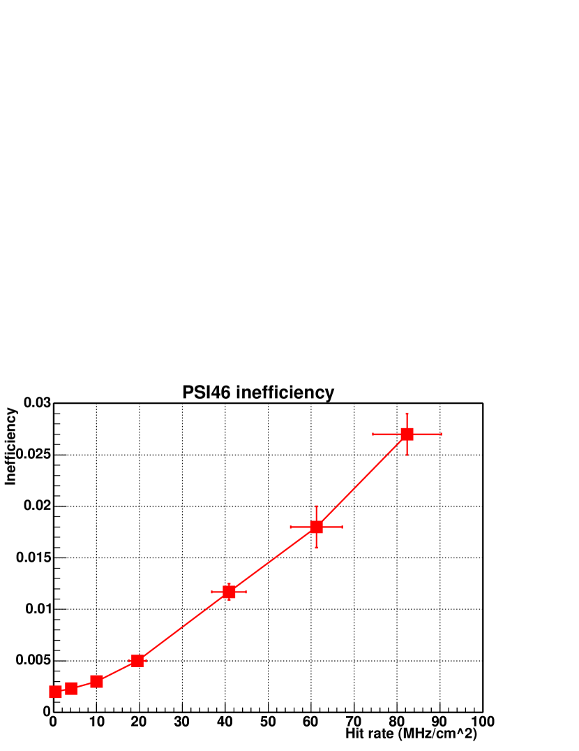
The inefficiency of the readout chip as a function of the track rate has been measured in a testbeam experiment as shown in Fig. 3 [8]. As the conditions there are slightly different from the final situation in CMS (impact angle is and particles are uncorrelated) it is difficult to relate this results to the LHC like conditions. However, the measured losses approximately agree with the simulations explained above.
2.2.2 Performance of the Present Readout Architecture at an upgraded LHC
With a further increase of the track rate when the luminosity is upgraded, the readout losses will also increase. As not all incefficiency mechanisms have the same rate dependence, a Monte-Carlo simulation was used to estimate the readout losses at a luminosity of cm-2s-1. To keep the time stamp buffer overflow losses below 1 % the number of buffers has to be increased from 12 to about 60. A similar scaling applies to the data buffers. The use of a very compact m technology would certainly help to limit the increase of the peripheral chip area.
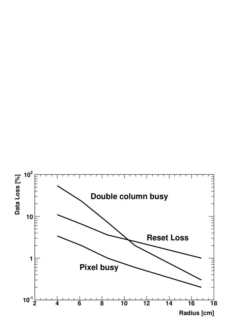
The dependency of the three remaining data loss mechanisms on the distance from the interaction point is shown in Fig. 4. With increasing particle rate (or decreasing radius) the probability of a double column to be hit more than three times during the time of a column drain increases dramatically. This limits the use of the present CMS-pixel readout at the tenfold LHC-luminosity to radii above 10 cm. For smaller radii a more elaborate redesign of the chip is necessary.
The reset loss does not increase as drastically with increasing particle rate as it mainly depends on the trigger latency and rate which are assumed to stay constant. The increase visible in Fig. 4 is due to the higher double column occupancy and the longer time necessary to read out the increased number of hits per triggered event.
The pixels are still small enough such that the probability to be hit twice within a short time (pixel busy) remains relatively low.
2.3 Cost Considerations
| Component | Costs [CHF] per | |
|---|---|---|
| module | cm2 | |
| 16 readout chips (m) | 400 | 40 |
| 1 Sensor (Si, n-in-n) | 700 | 65 |
| Bump bonding | 1200 | 110 |
| Fine-pitch hybrid (HDI) | 300 | 30 |
| Baseplate (Si3N4) | 50 | 5 |
| Cables and control chips | 250 | 25 |
| One Optical link | 250 | 25 |
| Sum | 3150 | 300 |
A rough cost estimate for a CMS pixel barrel module with an sensitive area of is given in Tab. 1. All the components added up lead to a price of roughly 300 CHF/cm2. This cost estimate ignores all off-module components like mechanics, cooling, cabling (not directly mounted on the detector modules), readout and control modules (in most cases VME), and power supplies. Those components contribute significantly to the total cost, but depend only weakly on the detector concept. If the present hybrid pixel technology is found to be the only possible one at fluences above , a configuration of three pixel layers at radii of 8, 11 and 14 cm is conceivable. They would add up to a total area of about 1.1 m2, assuming a 53 cm long barrel.
3 Pixel Detectors at intermediate Radii
At radii larger than 15 cm neither the track rate nor the radiation hardness represents a major limit for pixel detectors. As the area to be covered increases with the radius, cost issues become more important. The most effective items for a possible reduction are bump bonding and sensors (see Tab. 1).
The most cost driving requirement of the sensor’s n-in-n technology is the need of double sided processing. As the radiation hardness required at radii between 15 and 25 cm is still in the range of , the collection of electrons is more favourable. This naturally leads to n-in-p sensors, an option currently investigated by the RD50 collaboration [7]. It will require single sided processing only and might be available on 150 mm wafers. This offers the chance of getting three large modules (e.g. mm2) per wafer which might reduce the cost per area by more than a factor of three.
The disadvantage of the single sided process is that due to the absence of the guard rings on the back side, all sensor edges are at the potential of the applied bias voltage. As a consequence of the considerable radiation damage, high voltages (400-600 V) will be required to obtain a close to complete charge collection. Precautions to protect the readout electronics from destructive discharges will have to be taken, like e.g. the introduction of a thin Kapton film between readout chips and sensor edge.
Bumpbonding is in principle well established and widely used in industry. The cost driving requirement of particle physics is the small pitch below m. If this number is relaxed to a value above m, a wide range of cheap industrial packaging processes will become available (e.g. the IBM-C4 process [10]). The track density in this area will allow pixel areas of the order of m2. In addition the number of chip placements can be reduced by increasing the size of the readout chip to the largest practical dimensions (e.g. mm2).
The third most expensive component are the readout chips. The one-to-one coverage of the sensitive area with readout chips will be kept and savings can only be expected if the price of this kind of electronics further decreases with time.
The design of the detector modules has to be done under stringent cost constrains (e.g. choosing a more standard hybrid). If a level of roughly 100 CHF/cm2 is achieved, it will be possible to equip two layers, e.g. at 18 and 22 cm, with such detectors.
4 Pixel Detectors at Larger Radii
For the radial region between 25 and 60 cm an even more drastic cost reduction of pixel detectors is necessary which can only be reached if the full coverage of the active area with readout electronics is given up. This is possible because the suitable size of a sensing element is a few square millimeters while a readout channel can be integrated into an area of about mm2.
The shape of a sensing element (“mini strip” or “macro pixel”) could be m2 leading to about 10 000 channels per sensor. They could be read out by a small number of pixel chips with a much smaller cell size. The routing between the sensor cells and the inputs of the readout chips could be performed via a thick (about m) polyimide layer. An alternative would be the MCM-D technique [11] which in addition allows the integration of other components on a module. As the readout chips can be placed completely inside the active area of the sensor the sensor edges need not be kept on ground potential and a single sided sensor would be possible. Due to the moderate requirements in radiation hardness in this area () “traditional” and cheaply available DC-coupled p-in-n sensors can be used.
If it is possible to build such a detector for about 50 CHF/cm2, it is a good candidate for layers at radii of e.g. 30, 40 and 50 cm.
5 Conclusions
The main tasks of the CMS pixel detector are the measurement of displaced vertices and pattern recognition. The challenges in the hostile environment of LHC are the high level of radiation and the high rate of tracks. The requirements in particle detection efficiency and spatial resolution in CMS can be satisfied, however sometimes with little headroom.
In case of an LHC luminosity upgrade the increase of the track density will require the extension of pixel detectors to larger radii. Large areas, however, can only be equipped with pixel detectors whose cost is considerably reduced. A pixel system of 9 layers seems quite feasible:
- Innermost layer:
-
The requirements of the innermost pixel layer (roughly 4 cm) cannot be fullfilled with present technologies. Possible solutions are investigated by the RD50 collaboration. In addition the readout electronics for this environment has to be developed soon.
- Small radii:
-
The region starting from 8 cm can probably be equipped with present pixel modules with moderately modified readout chips. However, only binary spatial resolution can be reached.
- Intermediate radii:
-
For radii between 15 and 25 cm a less expensive pixel system with single sided sensors and industrial bumpbonding is proposed.
- Large radii:
-
Radii between 30 and 60 cm could be equipped with macropixels or ministrips.
If it is possbile to reach the targeted cost reduction such pixel systems will be very attractive for many other applications.
Acknowledgment
The authors would like to thank Kurt Gabathuler for useful discussions and the careful review of the manuscript.
References
- [1] The CMS Collaboration, CMS Tracker, Technical Design Report LHCC 98-6, CERN, Geneva, Switzerland (1998).
- [2] The CMS Collaboration, Addendum to the Tracker TDR, Technical Design Report LHCC 2000-016, CERN, Geneva, Switzerland (2000).
- [3] A. Dorokhov, et al., Test of silicon sensors for the CMS pixel detector, Nucl. Instrum. Methods A 530 (2004) 71–76.
- [4] EP-TH faculty meeting, CERN, 17.01.2001.
- [5] G. Lindström, et al., Radiation hard silicon detectors – developements by the RD48 (ROSE) collaboration, Nucl. Instrum. Methods A 466 (2001) 308–326.
- [6] T. Rohe, et al., Fluence dependence of charge collection of irradiated pixel sensors, Nucl. Instrum. Methods A 552 (2005) 232–238.
- [7] M. Bruzzi, et al., Radiation-hard semiconductor detectors for superLHC, Nucl. Instrum. Methods A 541 (2005) 189–201.
- [8] W. Erdmann, et al., The m front end for the CMS pixel detector, Nucl. Instrum. Methods A 549 (2005) 153–156.
- [9] D. Kotliński, Pixel detector data rates and inefficiencies, CMS Internal Note 2003/004, CERN, Geneva, Switzerland (2003).
- [10] L. F. Miller, Controlled collapse reflow chip joining, IBM J. of Res. Dev. 13 (1969) 239–250.
- [11] T. Flick, et al., Studies on MCM-D pixel-detector-modules, Nuclear Physics B - Proceedings Supplements 125 (2003) 85–89.