Laser nanotraps and nanotweezers for cold atoms: 3D gradient dipole force trap in the vicinity of Scanning Near-field Optical Microscope tip
Abstract
Using a two-dipole model of an optical near-field of Scanning Near-field Optical Microscope tip, i. e. taking into account contributions of magnetic and electric dipoles, we propose and analyze a new type of 3D optical nanotrap found for certain relations between electric and magnetic dipoles. Electric field attains a minimum value in vacuum in the vicinity of the tip and hence such a trap is quite suitable for manipulations with cold atoms.
pacs:
42.50.-p, 32.50.+dRecent enormous progress in the study of laser-cooled atoms and molecules put forward the problem of their using for quantum computing, frequency standard construction, and other technological applications (see e.g. [1-3]). To achieve this goal, as well as for the further progress of fundamental experiments in the field, new compact traps and new methods of “handling” the cold atoms, for example their transportation to/from a trap or between different traps, should be elaborated. An example of successful work in this direction is given e.g. by “atom-chip technology” experiments [4, 5], where guiding of cold atoms along the wires has been demonstrated. Further miniaturization of such devices is desirable. Ideally, one should have at his/her disposal true “single cold atom nanotweezers” which have very small sizes and only slightly perturb the trap. Evidently, the near-field optical configurations, based on subwavelength-size aperture in the apex of a sharp fiber tip or local field enhancement in the vicinity of sharp conducting tips (see e.g. [6, 7] for review on near-field optics) look rather promising. Hence it is not surprising that a number of near-field optical traps/tweezers have been proposed [7 - 15].
However, all of them have certain drawbacks and, we believe, this is the main reason why, to the best of our knowledge, none has been realized up to now. Putting aside the configurations where an extremum of the optical field is achieved on the surface of the tip [13] (configuration obviously inappropriate for atom trap), among these drawbacks we could mention that the traps proposed needed different hard-to-control non-optical interactions (centripetal potential, gravitational interaction, van der Waals force, etc.) to be closed, can be realized only in the non practical light reflection mode from the subwavelength aperture, and so on.
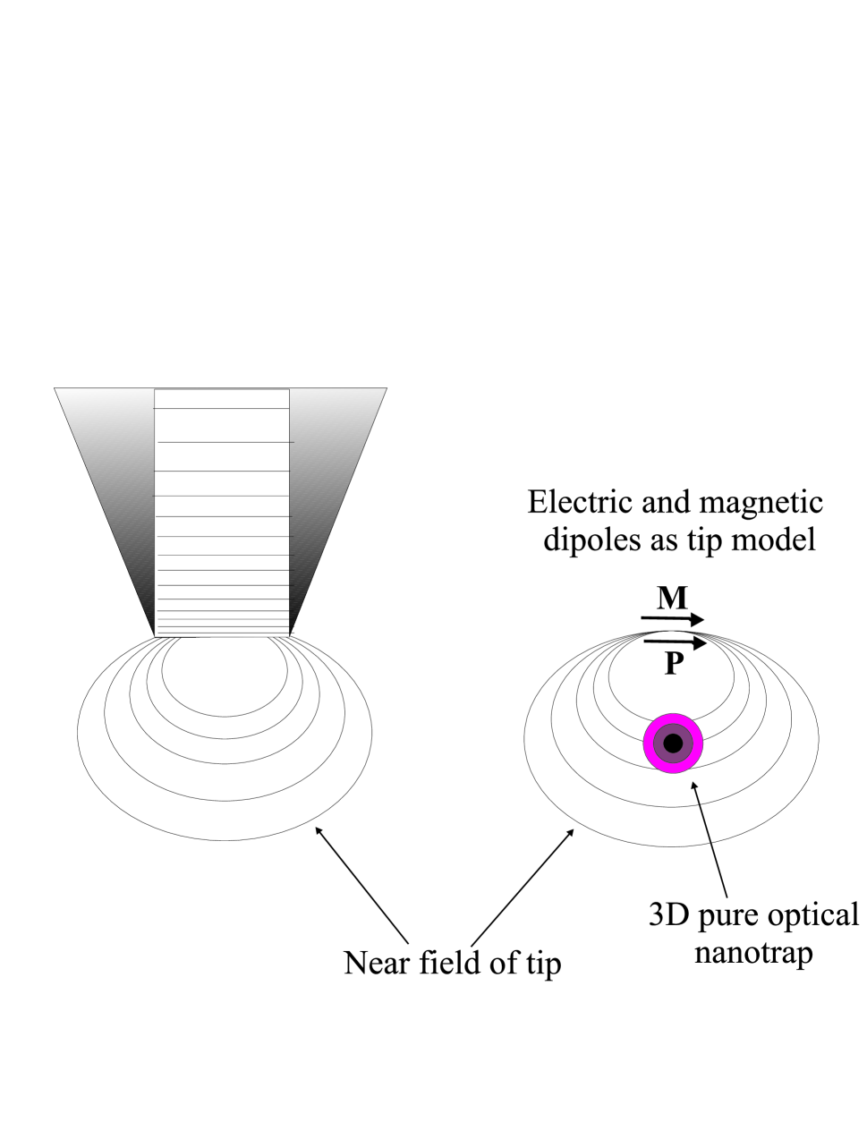
Here we propose and analyze the true “free standing”, or “support-free” purely optical 3D trap emerging in vacuum in the vicinity of an aperture of the Scanning Near-field Optical Microscope (SNOM) tip. The characteristic size of our trap is small in comparison with laser wavelength , so one indeed can speak about nanotrap. Because methods of Angstrom-precision motion of SNOM tip are well elaborated, the same construction is cold atom nanotweezers.
Our analysis is based on the two-dipole model of optical near field occurring in the vicinity of this tip, see Fig. 1. Such a model has been established recently, when it has been shown that in addition to the classic Bethe and Bouwkamp consideration, where in the case of normal incidence optical near field is modeled by one magnetic dipole M (see e.g. Refs. [16-18]), a field of an electric dipole P should be added to describe correctly optical near-field of a real fiber tip Drezet1 -Drezet2 . This effect is due mainly to the conical shape of the end area of such tip, and for a variety of tips and light polarizations different relations between the values and mutual orientations of M, P dipoles can be anticipated.
In near field of tip as in any laser fields, resonant atoms are subject to the optical dipole force with the potential Ashkin ,Letokhov :
| (1) |
Here is an atomic transition dipole moment, where is a natural line width, and is detuning between laser frequency and resonant frequency of an atom . Throughout the paper we consider the blue detuning , which results in atom trapping at the minimum of laser field intensity.It is well known that blue-detuned gradient force optical traps based on minimum of an electric field have essential advantages (they do not heat trapped atoms, etc.) in comparison with those based on maximum of an electric field using red-detuned light Letokhov .
To characterize the proposed 3D nanotrap let us consider electric field of light in the vicinity of a SNOM tip (i. e. in the near-field regions of both dipoles). Corresponding electric field of an electric dipole P has the form:
| (2) |
where R is the radius vector from the dipole position to an observation point. (SGCE units are used throughout the paper). Vector potential of a magnetic dipole M has the following form
| (3) |
and according to Faraday’s law electric field of this magnetic dipole in the near-field region has the form
| (4) |
where is wavevector in free space. When two dipoles are located at the same point {0,0,0}, intensity of total electric field behind an aperture can be presented in the form
| (5) |
Below we will speak about this value as about an “intensity” having in mind its obvious connection with the intensity of laser light “seeping” through the aperture of a SNOM tip: , where is speed of light .
It is naturally to look first for an axially symmetric trap. Such a trap occurs in particularly if
| (6) |
If these conditions hold true, expression for the intensity can be rewritten in the form
| (7) |
where and is the distance from the symmetry axis to an observation point.
Analysis shows that if we put the following additional condition on the dipole momenta
| (8) |
intensity (7) becomes equal to zero at the points
| (9) |
In its turn, it is possible to show that (8) will be satisfied in the case
| (10) |
It means that dipole momenta should be collinear to ensure the 3D trap.
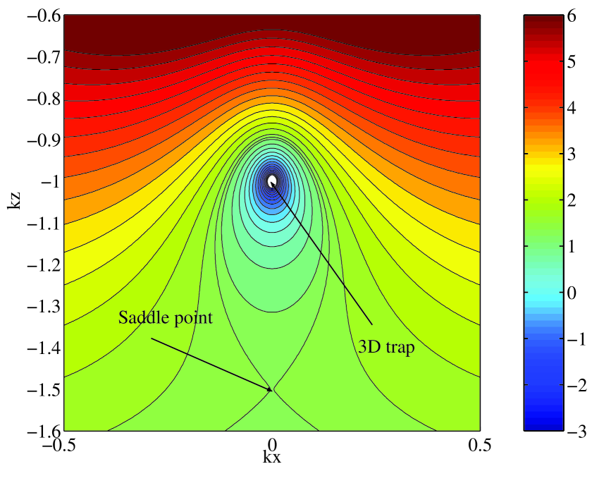
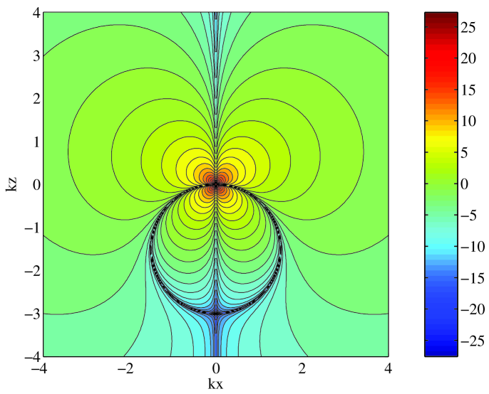
As intensity is a positive function of coordinates, zeros of intensity (9)correspond to true 3D minimum of an electric field. In Fig.2 the distribution of intensity in plane is shown for the case .
Intensity (7) has another point of extremum
| (11) |
which is a saddle point (see Fig. 2.). The value of intensity at this point is
| (12) |
This quantity can be used to estimate the potential well depth. For such an estimation one can use , where is an amplitude of the incoming light wave in aperture plane and is the radius of an aperture [16-19]. Substituting these values into (12), we get for the potential well depth
| (13) |
For modern tips and hence . For typical experimental conditions, an intensity of optical near field at the aperture of SNOM tip is about [6,7]. This means that e. g. for alkaline atoms, which are characterized by resonant dipole moments of the order of 10-17 SGSE and natural line widths (for example, for the 6S1/2–6P3/2 D2 transition of cesium atom at =852 nm, =8.0110-18 CGSE and Rafac ), traps with the depth of the order of a few milliKelvin, what is quite standard for optical dipole gradient force – based traps, can be realized when using , see (1). It is very important that under these conditions the trap will have about 10 energy levels of atomic motion with lowest level being about .
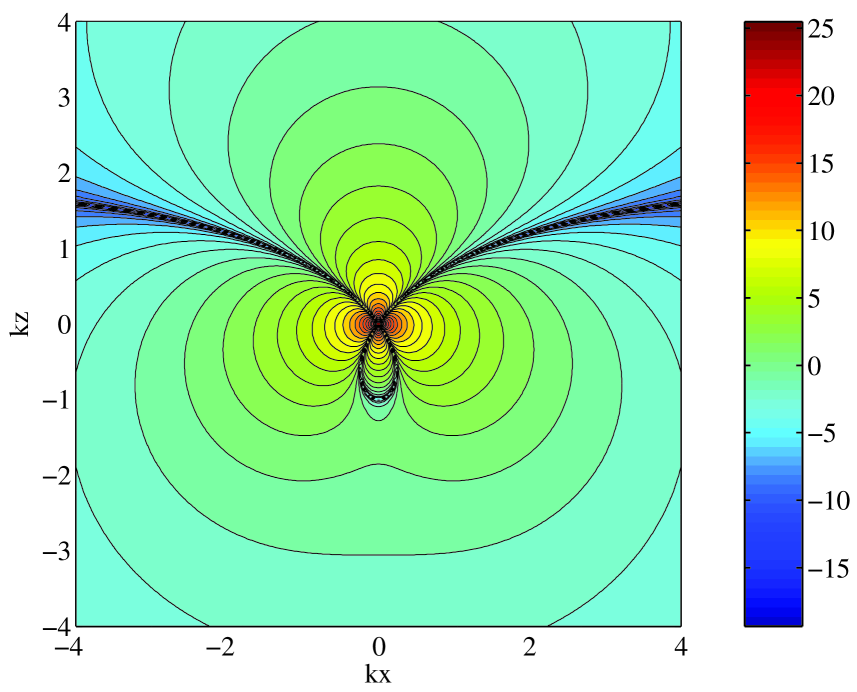
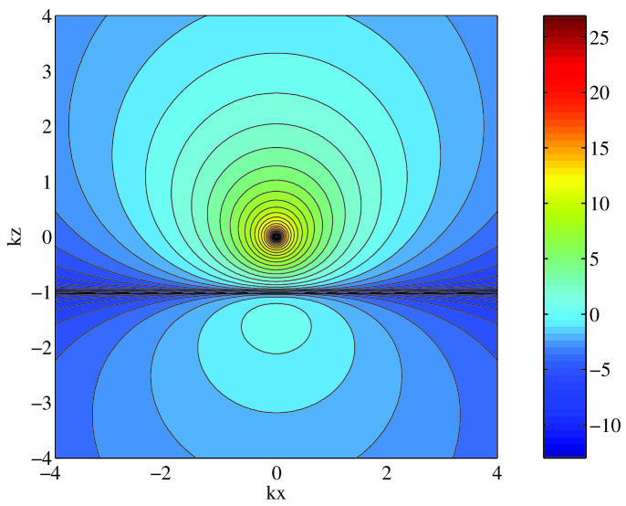
It is worthwhile to note, that existence of such a 3D trap is highly nontrivial, because the relevant field components have very complicated structure (see Figs. 3, 4, 5), and it seems very difficult to provide a minimum for their sum.
Mathematically, by varying P and M ratio and other parameters of the problem, our trap can be placed at any point on the symmetry axis. However, the two dipole approximation used is not valid very close to the aperture plane . Its validity starts from , where is the radius of an aperture. Hence we should consider only such parameters where the trap position occurs not too close to the aperture plane. Besides the condition allows us to neglect van der Waals attractive force which is always important in close vicinity of tip surface.
For our trap the minimum of intensity is stable against small perturbations. For example, if relation between the dipole values is
| (14) |
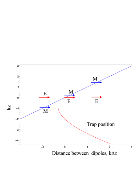
then true 3D minimum still exists provided or . Small variations of z-components of momenta ( and also result in small variations of trap position. Small mutual displacements (splitting) of dipoles in axial and/or radial directions also result in variation of the trap. In the case when magnetic dipole is moving away from the trap, that is in the case when electric dipole is placed between the trap and the magnetic one, the trap suffers only minor shifts. In the case when magnetic dipole is placed between an electric one and the trap, the intensity minimum disappears for large enough splitting, see Fig.6.
The retardation effects in the near field region generally are small. Nevertheless to estimate their influence let us consider the full electric field of electric and magnetic dipoles:
| (15) |
Analysis shows that for such a case 3d trap survives only when . Positions of the trapping region and the saddle point are given respectively by the formulae
| (16) |
and
| (17) |
Intensity at the bottom of the potential well is now nonzero
| (18) |
while the intensity at the saddle point is
| (19) |
These values determine the depth of our trap. Comparing results (16)-(19), where retardation effects are taken into account, with the quasistatic results (11) we see that in the case of magnetic dipole domination the position of the trap remains in the near field region and hence the retardation effects have only minor influence. On the other hand, in the case of substantially large amplitude of electric dipole, the retardation effects destroy our trap.
Hence we have shown that minimum of an electric field with the size smaller than the light wavelength and depth of a few milliKelvin did occur in vacuum in the vicinity of a SNOM tip. This minimum is stable against perturbations and can be tuned both in position and depth by changing relation between and and incident light electric field amplitude E0. This attests the trap proposed as a very promising basic element for future cold atom nanotraps and nanotweezers. Finally, we would like to note the following. Despite the two dipole model of optical near-field, whose using is inherent to obtain the reported results, nowadays seems is well established and supported by experiments [19-21], complete and rigorous analysis of all possible dipole configurations occurring for near field of a real tip is still lacking. In particular, the conditions to be imposed on experimental setup to obtain the trapping configuration of magnetic and electric dipoles also remain to be understood. Nevertheless, we believe that broad possibilities to vary SNOM tip shapes and coatings [6, 7] as well as to vary other parameters (e. g. incoming light polarization) give enough hope for practical realization of such a configuration. Indeed, it can quite happen that this is already done at least for one of plenty of the tips demonstrated up to date.
Acknowledgements.
The authors are grateful to Swiss National Science Foundation and Russian Foundation for Basic Research (V.V.K., grant # 04-02-16211) for financial support of this work.References
- (1) R. Folman, P. Kruger, J. Schmiedmayer, J. Denschlag, and C. Henkel, Adv. At. Mol. Opt. Phys., 48 (2002) 263.
- (2) M. Nielsen, I. Chuang, Quantum computation and quantum communication, Cambridge, Cambridge Univ. Press, 2000.
- (3) T. Calarco, H.-J. Briegel, D. Jakch, J. I. Cirac, and P. Zoller, J. Mod. Opt., 47 (2000) 2137.
- (4) P. Kruger, X. Luo, M. W. Klein, K. Brugger, A. Haase, S. Wildermuth, S. Groth, I. Bar-Joseph, R. Folman, J. Schmiedmayer, Phys. Rev. Lett., 91 (2003) 233201.
- (5) W. Hänsel, J. Reichel, P. Hommelhoff, and T. W. Hänsch, Phys. Rev. Lett., 86 (2001) 608.
- (6) R. C. Dunn, Chem. Rev., 99 (1999) 2891.
- (7) M. Ohtsu, Near-field nano/atom optics and technology. Tokyo, Springer, 1998.
- (8) M. Ohtsu, S. Jiang, T. Pangaribuan, K. Kozuma, in : D. W. Pohl, D. Courjon (Eds.), Near-field Optics, Kluwer, Dordrecht, 1993, p. 131.
- (9) H. Hori, in : D. W. Pohl, D. Courjon (Eds.), Near-field Optics, Kluwer, Dordrecht, 1993, p. 105.
- (10) V. V. Klimov, V. S. Letokhov, Opt. Commun., 121 (1995) 130.
- (11) V. V. Klimov, V. S. Letokhov, JETP Lett., 61 (1995) 13.
- (12) H. Ito, M. Ohtsu, Tech. Dig. 5th Int. Conf. Near-field Opt., Shirahama, Japan, 1998, p. 268.
- (13) L. Novotny, R. X. Bian, X. S. Xie, Phys. Rev. Lett. 79 (1997) 645.
- (14) S. K. Sekatskii, B. Riedo, G. Dietler, Opt. Commun. 195 (2001) 197.
- (15) V. I. Balykin, V. V. Klimov, V. S. Letokhov, JETP Letters, 78 (2003) 8; Optics and Photonic news, March 2005 ,p.44-48
- (16) H. A. Bethe, Phys. Rev., 66 (1944) 163.
- (17) C. J. Bouwkamp, Philips Res. Rep., 5 (1950)401.
- (18) V. V. Klimov, V. S. Letokhov, Opt. Commun., 106 (1994) 151.
- (19) A.Drezet, J. C. Woehl, S. Huant, Phys. Rev. E, 65 (2002) 046611.
- (20) C.Obermüller, K. Karrai, Appl. Phys. Lett., 67 (1995) 3408.
- (21) A.Drezet, M. J. Nasse, S. Huant, J. C. Woehl, Europhys. Lett., 66 (2004) 41.
- (22) J. P. Gordon, A. Ashkin, Phys. Rev. A, 21 (1980) 1606.
- (23) V. G. Minogin, V. S. Letokhov, Laser Light Pressure on Atoms, Gordon and Breach, New York, 1987.
- (24) R. J. Rafac, C. E. Tanner, A. E. Livingston, K. W. Kukla, H. G. Berry, C. A. Kurtz, Phys. Rev. A, 50 (1994) R1976.