Near-field spectroscopy of bimodal size distribution of InAs/AlGaAs quantum dots
Abstract
We report on high-resolution photoluminescence (PL) spectroscopy of spatial structure of InAs/AlGaAs quantum dots (QDs) by using a near-field scanning optical microscope (NSOM). The double-peaked distribution of PL spectra is clearly observed, which is associated with the bimodal size distribution of single QDs. In particular, the size difference of single QDs, represented by the doublet spectral distribution, can be directly observed by the NSOM images of PL.
pacs:
68.37.Uv, 78.55.Cr, 78.67.HcSelf-assembly growth process has raised interesting questions regarding the growth dynamics of quantum dots (QDs) and the resulting size and shape distributions. aplmo ; japliu ; woojap The size uniformity of InAs/GaAS QDs is typically broken beyond QD deposition of more than 2.0 monolayer, which is characterized by the bimodal or multimodal QD distribution. jvcQDsize ; aplQDsizebr In previous works, the spatial structures of the bimodal QD systems have been investigated by observing photoluminescence (PL) at various conditions of QD coverage growth. prbbimodal ; prbQDsize ; japQDsize ; jvcQDsize ; japQDsizek These results have been valuable for understanding optical properties of QD ensemble structures grown with various coverage thickness. However, it is difficult to acquire a high spatial as well as spectral resolution of single QDs in bimodal QD system if far-field optical spectroscopy is employed. Several experiments have been performed by using a near-field scanning optical microscope (NSOM) for nano-scale optical measurement of semiconductor QD structures. nearapl ; saikiprl ; yjyuapl ; mapl Such a unique capability may allow a detailed study of individual QDs that are grown under various structure conditions. In this Letter, we report on the observation of high-resolution near-field laser spectroscopy of bimodal QD size distributions in the high-density InAs/AlGaAs QD structures.
High density (5.5 1010 cm-2) InAs QDs, embedded in 50-nm AlGaAs cladding layers with a 5-nm GaAs capping layer, were grown by molecular beam epitaxy. The InAs/AlGaAs QD structure was grown on a 100-nm-thick GaAs buffer layer deposited on a GaAs (100) substrate. woojap This structure confines strongly charge carriers within single QDs due to the large energy difference between InAs QDs and AlGaAs barriers. However, the size uniformity of QDs is not so good due to the strain induced by lattice mismatch between InAs QDs and AlGaAs barriers. Thus the size distribution and deposition thickness of InAs single QDs is not uniform and depends on the specific location of nano-scale region on the sample, even though the average coverage of InAs is about 2.3 monolayer.
For optical pumping of QDs, a Ti:sapphire laser, operated at the photon energy of 1.67 eV, was used. The excitation laser light was coupled to a single-mode optical fiber and guided to a chemically etched sharp fiber tip on which a 100-nm gold-coated aperture was fabricated. jasco Such a nano-scale light source, generated by an apertured fiber probe, made it possible to excite single InAs QDs in small area with nano-scale position selectivity. The resulting PL signal was collected by the same fiber so that any loss of spatial resolution due to diffusion could be minimized. eahapl ; yjyuapl ; matapl Both the sample and the apertured fiber probe were enclosed in a He-flow-type cryostat and kept at 10 K. The PL signal was dispersed by a 0.3 m single monochromator with a spectral resolution of 0.3 meV and detected by a liquid-nitrogen-cooled charge coupled device camera to accomplish the high signal-to-noise ratio.
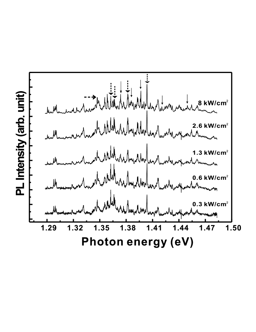
Figure 1 shows the time-integrated, high-resolution PL spectra collected for 10 s at each excitation power density from 0.3 to 8 kW/cm2. We have observed many sharp PL peaks of single QDs, with an average linewidth of about 0.7 meV. It is found that the PL intensity, resulting from the ground state (dotted arrows), is saturated as the excitation power density is increased. The PL from the excited state (solid arrows), on the other hand, emerges and its intensity increases with excitation power.
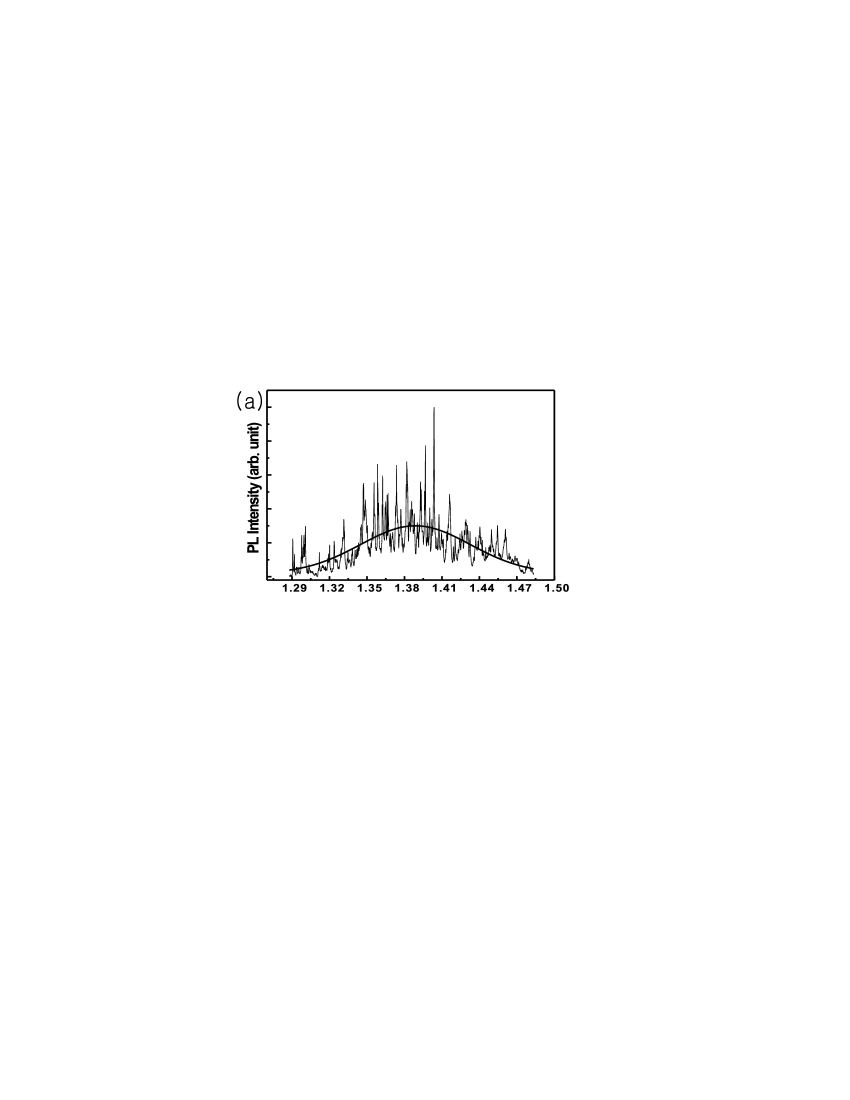
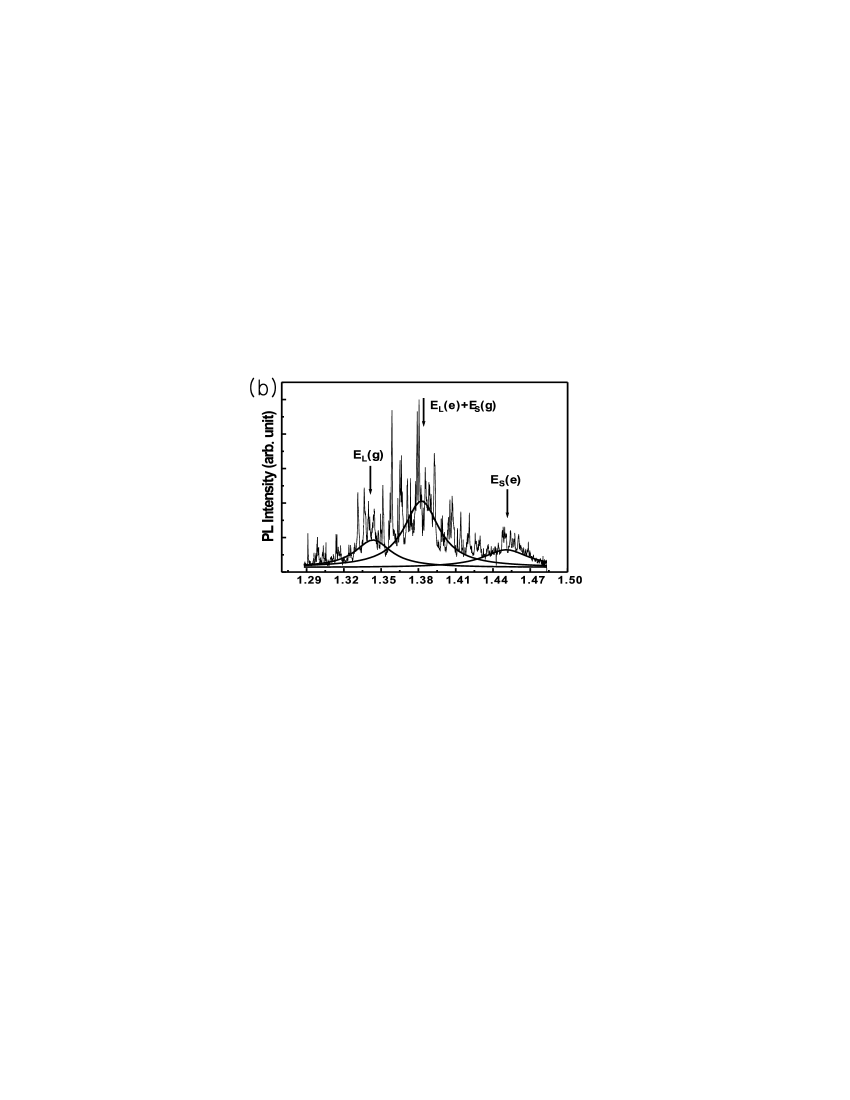
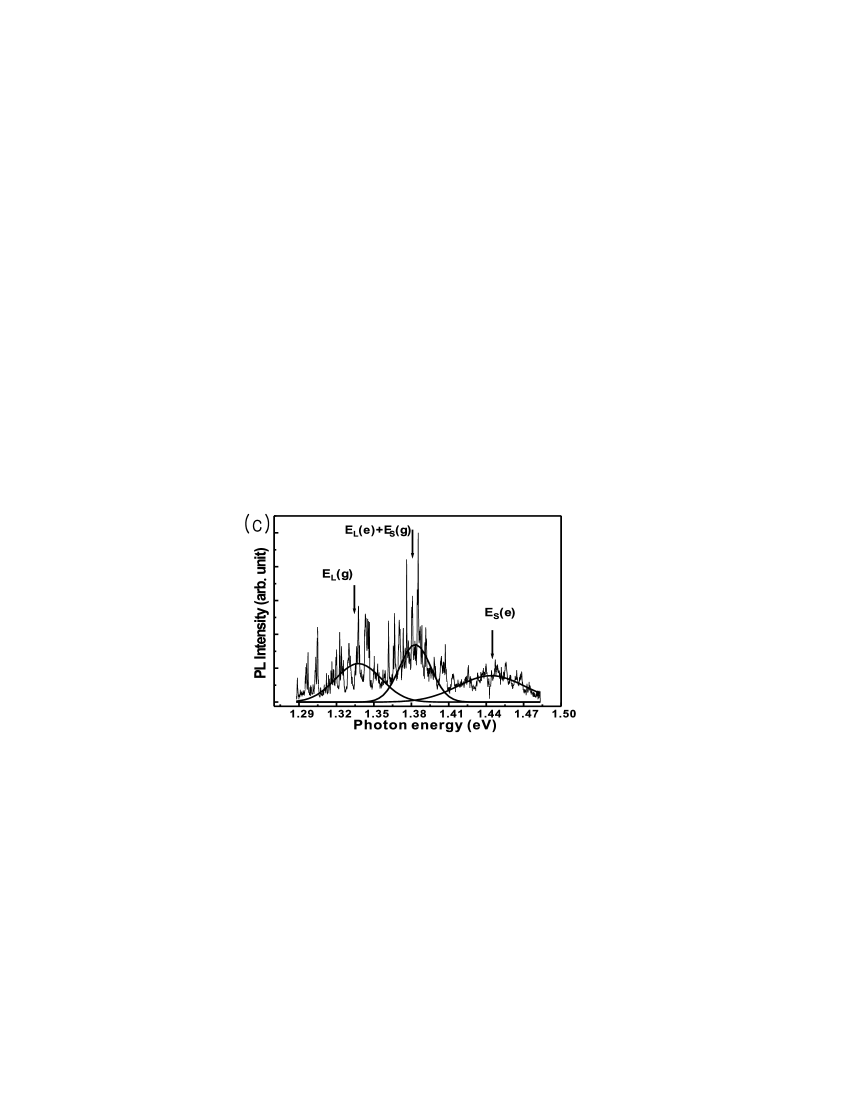
Figure 2 shows the time-integrated PL spectra collected for 10 s, obtained at different positions on the same sample with 8 kW/cm2 excitation power density. In Fig. 2(a), the PL peaks may be fitted by one Gaussian distribution, which is the same as that obtained at the excitation power density of 8 kW/cm2 in Fig. 1. However, the PL spectrum in Fig. 2(b), obtained at a different position, could be decomposed into two Gaussian distributions (centered at 1.34 eV and 1.38 eV, respectively) and a shoulder (centered at 1.45 eV). The similar PL peaks in Fig. 2(c) can be relatively clearly divided into two dominated Gaussian distributions (centered at 1.33 and 1.38 eV, respectively) and a shoulder (centered at 1.45 eV). This feature of Gaussian distributions shown in Figs. 2(b) and (c) are the characteristic fingerprints of the bimodal size distributions of single QDs, obtained in far-field PL experiments on the samples having various QD thickness. aplQDsizebr ; aplQDsizeha ; prbQDsize ; prbbimodal ; japQDsize ; jvcQDsize ; japQDsizek Note that the reported energy interval between doublet-like features of far-field PL spectra due to the bimodal-sized QDs was about several tens meV, japQDsize ; aplQDsizebr ; prbQDsize as similarly observed in our experiment.
Each PL spectrum, which can be fitted into three groups by Gaussian functions as in Figs. 2(b) and (c), can be attributed to two contributions of QD size distribution. The first group is the lowest energy distribution (centered at 1.33 eV in Fig. 2(b) and 1.34 eV in Fig. 2(c)), which is associated with the ground states of large-sized QDs (EL(g)). And the second one, represented by the middle energy group (centered at 1.38 eV in Fig. 2(b) and (c)), is contributed by the excited states of large-sized QDs (EL(e)) as well as the ground states of small-sized QDs (ES(g)). The last group is the shoulder group, centered at 1.45 eV in Fig. 2(b) and (c), comes from the excited states of small-sized QDs (ES(e)), as also reported by other works. prbbimodal ; jvcQDsize
We may observe that the thickness of InAs QDs at the sample position in Fig. 2(b) and (c) is larger than that in Fig. 2(a), because it was obtained at the lower-energy PL peaks (EL(g)) in the doublet-like PL peak-distribution. The number of large-sized QDs in Fig. 2(c) is also considered to be larger than that in Fig. 2(b), because the Gaussian peak at EL(g) in Fig. 2(c) is lower by 10 meV and broader by 22 meV than that in Fig. 2(b). Here the center of energy state and linewidth of EL(g) Gaussian peaks are 1.34 eV and 33 meV [1.33 eV and 55 meV] in Fig. 2(b) [2(c)], respectively. Thus, we infer that the InAs QDs coverage on position in Fig. 2(c) is larger than in Fig. 2(b). This is the first time observation of varying the near-field PL spectra of bimodal size-distributed QDs on different InAs deposited positions of sample with such a high spectral resolving power.
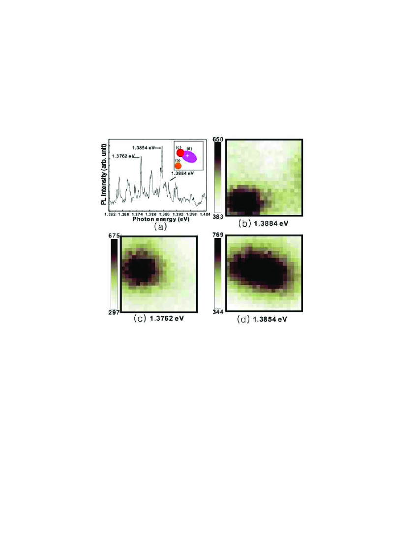
The PL spectrum from 1.362 eV to 1.404 eV in Fig. 2(c) is magnified and shown in Fig. 3(a). This spectrum was collected with a probe located at the center of scanning PL image area which was marked by a cross as illustrated in the inset of Fig. 3(a). Note that there are EL(e) peaks and ES(g) peaks in this PL spectrum range (from 1.35 eV to 1.41 eV) in Fig. 2(c). We also obtain PL images of selected three PL peaks(1.3762 eV, 1.3854 eV, and 1.3884 eV) at the same area (500 nm500 nm) in Fig. 3(b), (c), and (d).
The data acquisition(DAQ) process is as follows:
(1)The 100 nm apertured probe is located on a selected sample position and PL spectrum is taken in the entire spectral range with a nitrogen-cooled CCD camera during 10 s.
(2)This DAQ process is repeated sequentially in all other pixels of the scanning area.
(3)Then, each PL image at a given energy level from the 400 data files is processed to obtain the corresponding energy and spatial spectrum of the InAs single QDs. eahapl
The FWHM of horizontal cross section axis on the PL images in Fig. 3(b), (c), and (d) are about 200 nm, 260 nm, and 400 nm, respectively. The large-sized single QD with anisotropic PL image in Fig. 3(d) is due to our growth condition that the average InAs deposition thickness is about 2.3 ML. Note that if the thickness of a deposited InAs layer is larger than 2.0 ML, large QDs with a diameter and height greater than that of the average single QDs size (in our case, 20 nm lateral dimension and 0.7-nm height) are created as in the previous observations. japliu ; jvcQDsize ; aplQDsizebr We have found that the size of single QD of 1.3854 eV is about twice larger than that of 1.3884 eV and 1.3762 eV PL peaks in Fig. 3. Therefore, it seems clear that each selective peaks were divided by EL(e) peaks(centered at 1.3854 eV) and ES(g) peaks(centered at 1.3884 eV, 1.3762 eV) with PL spectrum in Fig. 2(c) and PL images in Fig. 3. It is very difficult to discriminate the size difference of single QDs, which are grown in such a high density (5.5 1010 cm-2) and embedded in between barrier and cap layers. Nevertheless, we have distinguished single QDs with different size having selective PL energy states from the measured PL images obtained by using an NSOM.
In conclusion, we have observed the variation of high-resolution PL spectra associated with the size distribution depending on different locations of QDs structure. We also have characterized the size-difference of single QDs having PL peaks in doublet-like distribution by using the PL images obtained by an NSOM.
This work was supported by the Korean Ministry of Science and Technology through Creative Research Initiatives Program.
References
- (1) J. M. Moison, F. Houzay, F. Barthe, L. Leprince, E. Andr, and O. Vatel, Appl. Phys. Lett. 64, 196 (1994).
- (2) H. Y. Liu, B. Xu, Y. H. Chen, D. Ding, and Z. G. Wang, J. Appl. Phys. 88, 5433 (2000).
- (3) Y. S. Kim, U. H. Lee, D. Lee, S. J. Rhee, Y. A. Leem, H. S. Ko, D. H. Kim, and J. C. Woo, J. Appl. Phys. 87, 241 (2000).
- (4) S. J. Lee, S. K. Noh, J. W. Choe, and E. K. Kim, J. Crystal Growth 267, 405 (2004).
- (5) L. Brusaferri, S. Sanguinetti, E. Grilli, M. Guzzi, A. Bignazzi, F. Bogani, L. Carraresi, M. Colocci, A. Bosacchi, P. Frigeri, and S. Franchi, Appl. Phys. Lett. 69, 3354 (1996).
- (6) Y. C. Zhang, C. J. Huang, F. Q. Liu, B. Xu, J. Wu, Y. H. Chen, D. Ding, W. H. Jiang, X. L. Ye, and Z. G. Wang, J. Appl. Phys. 90, 1973 (2001).
- (7) H. Kissel, U. Müller, C. Walther, W. T. Masselink, Y. I. Mazur, G. G. Tarasov, and M. P. Lisitsa, Phys. Rev. B 62, 7213 (2000).
- (8) K. H. Schmidt, G. Medeiros-Ribeiro, U. Kunze, G. Abstreiter, M. Hagn, and P. M. Petroff, J. Appl. Phys. 84, 4268 (1998).
- (9) S. Anders, C. S. Kim, B. Klein, M. W. Keller, R. P. Mirin, and A. G. Norman, Phys. Rev. B 66, 125309 (2002).
- (10) H. Lee, R. Lowe-Webb, T. J. Johnson, W. Yang, and P. C. Sercel, Appl. Phys. Lett. 73, 3556 (1998).
- (11) K. Matsuda, T. Saiki, S. Nomura, M. Mihara, Y. Aoyagi, S. Nair, and T. Takagahara, Phys. Rev. Lett. 91, 177401 (2003).
- (12) A. Chavez-Pirson, J. Temmyo, H. Kamada, H. Gotoh, and H. Ando, Appl. Phys. Lett. 72, 3494 (1998).
- (13) Y.-J. Yu, W. Jhe, and Y. Arakawa, Appl. Phys. Lett. 83, 3024 (2003).
- (14) M. Hadjipanayi, A. C. Maciel, J. F. Ryan, D. Wasserman, and S. A. Lyon, Appl. Phys. Lett. 85, 2535 (2004).
- (15) M. Ohtsu, Near-Field Nano/Atom Optics and Technology (Springer-Verlag, 1998).
- (16) T. Saiki, and K. Matsuda, Appl. Phys. Lett. 74, 2773 (1999).
- (17) S.-K. Eah, W. Jhe, and Y. Arakawa, Appl. Phys. Lett. 80, 2779 (2002).
- (18) Y. Temko, T. Suzuki, P. Kratzer, and K. Jacobi, Phys. Rev. B 68, 165310 (2003).