Modeling of a Resonant Tunneling Diode Optical Modulator
Abstract
The integration of a double barrier resonant tunneling diode within a unipolar optical waveguide provides electrical gain over a wide bandwidth. Due to the non-linearities introduced by the double barrier resonant tunneling diode an unipolar InGaAlAs/InP optical waveguide can be employed both as optical modulator and optical detector. The modeling results of a device operating as optical modulator agree with preliminary experimental data, foreseeing for an optimized device modulation depths up to 23 dB with chirp parameter between -1 and 0 in the wavelength range analyzed (1520 nm - 1600 nm).
I Introduction
Due to their high-speed response and radio frequency (rf) gain, several groups have proposed the application of resonant tunnelling diodes (RTDs) in the optical and infrared domains Mizuta .
A novel optoelectronic device based on the integration of a RTD with an optical waveguide (OW), the RTD-OW, as been proposed for electro-optical and opto-electrical conversion McMeekin . The waveguide configuration is used to ensure large interaction volume between the RTD regions and the guided light. The full demonstration and development of this new device concept in the ternary AlGaAs/GaAs and quaternary InGaAlAs/InP material systems can be of great importance for optical communication, specially in high-speed fibre radio links. The AlGaAs/GaAs material system is interesting for short hall communications in the wavelength range around 900 nm, and the InGaAlAs/InP material system is useful in the wavelength range where optical fibres have the lowest loss and chromatic dispersion (1300 nm to 1600 nm).
Our group has successfully integrated AlGaAs and InGaAlAs RTDs within unipolar AlGaAs/GaAs and InGaAlAs/InP optical waveguides, respectively, and demonstrated optical modulation of guided light around 900 nm and 1550 nm Figueiredo1 Figueiredo2 . In this paper we report modeling results of the device operating as an electro-optical converter at 1550 nm, confirms preliminary experimental data Figueiredo2 Figueiredo3 .
II Principle of operation as a modulator
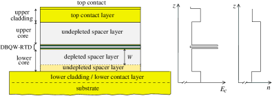
Essentially, the RTD-OW is a unipolar device consisting of a double barrier quantum well (DBQW) resonant tunneling diode (RTD) embedded within a ridge channel optical waveguide. The DBQW-RTD structure consists of two AlAs barriers surrounding a InGaAs quantum well. The optical waveguide comprehends two moderately n-doped InGaAlAs layers lattice matched to InP, sandwiched between highly n-doped InP cladding regions, Fig. 1.
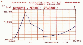
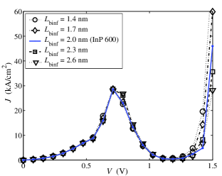
The presence of the DBQW-RTD within the waveguide core introduces high nonlinearities in the current-voltage (I-V) characteristic of the unipolar waveguide: the device I-V curve shows large negative differential resistance (NDR), Fig. 2. The physics that gives rise to this type of I-V is explained in Figueiredo2 .
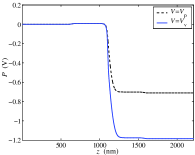
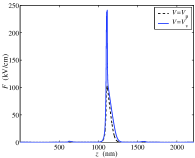
As a consequence of the presence of the RTD within the unipolar waveguide core a non-uniform potential distribution is induced across the waveguide cross-section, Fig. 3. The magnitude of the associated electric field distribution depends strongly on the bias voltage. When the device operating point switches from the peak to the valley regions of the I-V curve there is an enhancement of the electric field across the waveguide depletion region. This produces substantial changes in the absorption coefficient of the waveguide at wavelengths near the core material band-edge via the Franz-Keldysh effect (for more details see Figueiredo2 ). The operation of the RTD-OW as an optical modulator takes advantage of this absorption change induced by the RTD peak-to-valley switching.

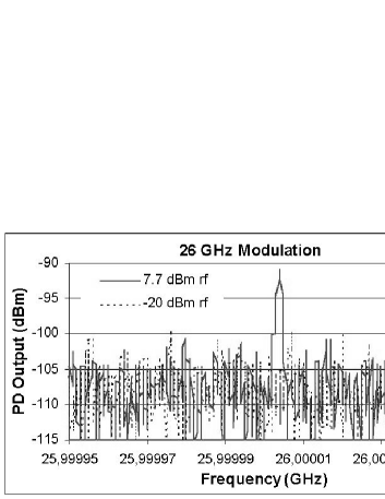
Preliminary experimental results indicate that a non-optimized device designed to act as a modulator is capable of high-speed modulation (up to 26 GHz) with extinction ratio higher than 10 dB over a wide range of wavelengths at driving power as low as 7.7 dBm, Fig. 4 Figueiredo3 .
III Device modeling phases
The device modeling comprehends two phases. In the first, the electrical characteristics of the device such as the I-V curve and the potential distribution across the waveguide cross-section are determined. In the second part, the waveguide optical properties induced changes such as the extinction coefficient and the refractive index variations at different bias voltage and as function of the guided light wavelength are calculated.
The RTD-OW electrical modelling employs the WinGreen simulation package WinGreen that determines the device I-V characteristic and the potential profiles across the waveguide cross-section as function of the applied bias. The I-V curve permits to extract the NDR region characteristics: the peak and the valley voltages, Fig. 5.
(a)
(b)
The electric field distribution across the waveguide for a given bias voltage , Fig. 6b), is obtained through the gradient of the potential distribution, Fig. 6a).
(a) (b)
The waveguide absorption coefficient at a given voltage is then determined as a function of the electric field distribution , in V/cm, and of the light energy , in eV, using the Franz-Keldysh relation Chuang ,
| (1) |
where Ai is the Airy function, , , , is the core band-gap energy expressed in eV, and is the refractive index; and are the electron-hole reduced effective mass and electron rest mass, respectively; is a scaling parameter to adjust Eq. 1 to independent experimental data Chuang . The sum is over the light and heavy holes.
The absorption change due to the RTD peak to valley switching is then given by:
| (2) |
where represents the magnitude of the electric field at the peak (p) and at the valley (v), respectively.
The refractive index change as function of the bias is determined from the absorption change through the Kramers-Kronig relation Chuang
| (3) |
The modulation depth is estimated through
| (4) |
where represents the overlap integral between the electric field and the optical field distributions. The chirp parameter is calculated using the relation
| (5) |
where is the extinction coefficient, given by .
IV Modeling results
The objective of this work is to understand the role of the structural and material parameters on the device performance in order to determine the optimized device structure for each application. The study reported here aims the determination of the RTD-OW structure that gives the highest modulation depth with the minimum propagation loss. To achieve this purpose it is necessary to maximize the electric field change when the device operation point switches from the peak to the valley region and the overlap between the electric field distribution and the guided mode.
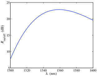
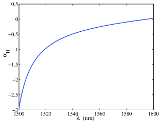
According the modeling results, the optimized modulator structure corresponds to a RTD-OW configuration consisting of two 2 nm thick AlAs barriers surrounding a 6 nm thick InGaAlAs quantum well, symmetrically embedded within a 300 mm unipolar InGaAlAs waveguide core with doping concentration of cm-3 and 600 nm thick InP cladding layers highly doped ( cm-3). A 200 m long RTD-OW shows extinction ratio up to 23 dB around 1560 nm with chirp parameter of -0.25, Fig. 7. The results also show the propagation loss are considerable higher than the “best” values reported in the literature. The way to decrease the propagation loss are under current investigation.
(a)
(b)
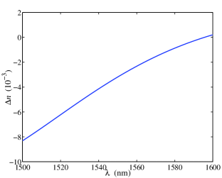
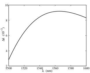
The refractive index change and the extinction coefficient variation are shown in Fig. 8, and appears to indicate the RTD-OW has high potential to operate as an electro-refraction modulator through an interferometer configuration.
(a)
(b)
V Conclusion and future work
The modeling results corroborate preliminary modulation depth experimental data Figueiredo2 Figueiredo3 . The fabrication of devices based on the present optimized structures is being considered.
The current devices also show detection capabilities. Its is foreseen the device can operate as a light detector incorporating an intrinsic integrated amplifier for the photocurrent generated by the incident light. The presented model is currently being extended to include the effect of light absorption.
Acknowledgment
This work is supported by the Fundação para a Ciência e a Tecnologia (Portugal) under Grant No. POSI/41760/CPS/2001.
References
- (1) I. Gravé, S. C. Kan, G. Griffel, S. W. Wu, A. Sa’ar, and A. Yariv, “Monolithic integration of a resonant tunneling diode and a quantum well semiconductor laser,” Appl. Phys. Lett., Vol. 58, pp. 110-112, 1991; K. Sano, K. Murata, T. Akeyoshi, N. Shimizu, T. Otsuji, M. Yamamoto, T. Ishibashi and E. Sano,“Ultra-fast optoelectronic circuit using resonant tunnelling diodes and uni-travelling-carrier photodiode,” Electron. Lett., Vol. 34, pp. 215-217, 1998.
- (2) S.G. McMeekin, M.R. Taylor, B. Vogele, C.R. Stanley, C.N. Ironside, “Franz-Keldysh effect in a optical waveguide containing a resonant tunnelling diode,” Appl. Phys. Lett., Vol. 65, pp. 1076-1078, 1994.
- (3) J. M. L. Figueiredo, C. R. Stanley, A. R. Boyd, C. N. Ironside, S. G. McMeekin, and A. M. P. Leite, Optical modulation in a resonant tunneling relaxation oscillator, Appl. Phys. Lett., Vol. 74, pp. 1197-1199, 1999.
- (4) J. M. L. Figueiredo, C. N. Ironside, and C. R. Stanley, “Electric field switching in a resonant tunnelling diode electroabsorption modulator,” IEEE J. Quant. Electron., Vol. 37, pp. 1547-1552, 2001.
- (5) J. M. L. Figueiredo, C. N. Ironside, and C. R. Stanley, “Ultralow voltage resonant tunnelling diode electroabsorption modulator,” J. Modern Optics, Vol. 49, pp. 939-945, 2002.
- (6) The WinGreen simulation package, http://www.fz-juelich.de/isg/mbe/software.html.
- (7) S.L. Chuang, Physics of Optoelectronic Devices, Wiley & Sons 1995.