Simulation study of electron drift and gas multiplication in Micro Pixel Chamber
Abstract
The physical processes of charge collection and gas multiplication of a Micro Pixel Chamber (-PIC) were studied in detail using a three-dimensional simulation. The collection efficiencies of primary electrons and gas multiplication factors were calculated for several electrode structures. Based on those studies, we analyzed the optimization of the electrode structure of the -PIC, in order to obtain a high gas gain of more than and a simultaneous suppression of discharges. Consequently, we found that these characteristics strongly depend on the substrate thickness and the anode diameter of the -PIC. In addition, a gas gain of would be expected for a -PIC having a thick substrate of .
keywords:
Gaseous detector; Micro-Pattern detector; Imaging; 3D simulation;, , , , , , , , , ,
1 Introduction
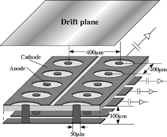
The Micro Pixel Chamber (-PIC) is a recently developed gaseous two-dimensional imaging detector [1]. The schematic structure is shown in Fig. 1. The -PIC is a double-sided Printed Circuit Board (PCB) with a thick polyimide substrate. We developed a -PIC with a detection area. On the front and rear sides of the substrate, 256 cathode and 256 anode strips are formed orthogonally with a pitch of , respectively. A cathode strip has circular openings of diameters with a pitch of . Anode pillars of 50 diameters are formed on anode strips through the substrate at the center of each cathode openings. We have made several -PICs with various electrode structures and studied their performances [2]. Consequently, a gas gain of and long-term stability with a gas gain of have been realized [3]. A position resolution of was also obtained [4].
Although the electrode structure of the -PIC reminds that of a Microdot chamber (MDOT) [5], its production method is quite different, and thus the -PIC has an advantage of a thick substrate. In a MDOT detector, which has a very thin () insulator layer, the electric field near to the surface of the substrate seems to be distorted by the buried readout buses [6]. On the contrary, this effect is weakened by the thick substrate in the -PIC. In this paper, we studied in detail the dependence of the electric field on the substrate thickness by a three-dimensional simulation. We reveal the operation principle and features of the -PIC, and discuss the optimization of the electrode structure.
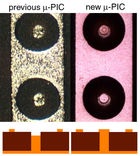
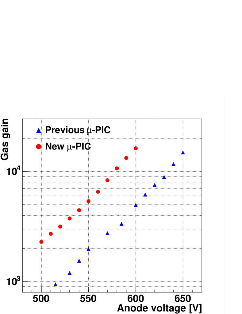
In our previous simulation work [8], we found that the gas gain was degraded because the top of the anode pillars are below the substrate; , the collection efficiency of primary electrons was about 30%. With this previous structure, two thirds of the drift electrons ended on the substrate, only the rest contributing the observable gas gain. In addition, these electrons attached on the surface possibly caused discharges. In order to solve these problems, we have developed a -PIC with a new manufacturing technology [7]. The anode electrodes of this new type -PIC are uniformly formed to above the substrate surface. Microscopic photographs and schematic cross sections of the previous and this new -PICs are shown in Fig. 2. The measured gas gain was three times higher than that of the previous -PIC, as shown in Fig. 3(a), which was consistent with the simulation results [8]. Detailed performance studies of this new -PIC is reported elsewhere [4]. This result shows that the three-dimensional simulation is a reliable method to study the geometrical structures of the -PIC. Therefore, we study the operation principles quantitatively and investigated the optimum structure of the -PIC with a three-dimensional simulation.
2 Simulation method
2.1 Codes
Simulation studies were carried out using Maxwell 3-D field simulator (Maxwell) [9] and Garfield [10]. The electromagnetic field in a three-dimensional structure was calculated using a finite element method (FEM) by Maxwell. Maps of the electric field, voltage, and dielectric constant were generated by the Maxwell for the unit cell of the -PIC, which is represented as a mesh consisting of fine tetrahedrons. A unit cell is 400400 in size and consists of a polyimide substrate with a relative dielectric constant of 3.5 and a pair of anode and cathode electrodes.
These maps were then fed to Garfield, and the dynamics of the drift electrons were simulated. Primary electrons were uniformly generated in the unit area 400 above the substrate, and the drift paths of electrons were calculated by the Monte Carlo method. The absolute multiplication factor was calculated as an exponentiated integral of the first Townsend coefficient along the drift path,
| (1) |
where is the first Townsend coefficient. The Townsend coefficient of the gas mixture was calculated using the Magboltz [11] program. Usually, some of the electrons do not reach the anodes, and hence the observed, or ”effective” multiplication factor is smaller than . We define , an electron collection efficiency by
| (2) |
In the simulation, we estimated by , where is the number of primary electrons collected by the anode, and is the total number of primary electrons that reached the detector surface. Because the observed gas gain, or the detector response, is determined by , we focus on in the following discussion.
2.2 Parameters
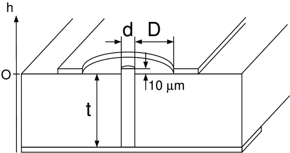
The geometrical parameters of the -PIC used for the simulation are listed below, where is the height from the surface of the substrate.
-
1.
Height of the anode electrode (fixed; at ),
-
2.
Width of the rear side anode strip (fixed; at ),
-
3.
Width of the cathode strip (fixed; ),
-
4.
Diameter of the cathode openings (fixed; ),
-
5.
Substrate thickness (variable; ),
-
6.
Diameter of the anode electrode (variable; ).
We examined the dependences on and , with all other parameters fixed. These geometrical parameters of the -PIC are described in Fig. 4. The anode-cathode voltage was 600V and the drift electric field was . The gas mixture was Ar/ (80/20).
3 Simulation results
3.1 dependence on the substrate thickness
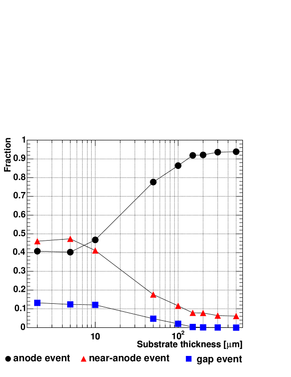
Some pixel type detectors were made by the IC technology and hence had a very thin insulator between metal layers (several ). Therefore, the electric field in the drift region near the surface of the substrate is affected by the readout strips buried in the substrate. Some of the drift electrons would be directed toward the readout buses, rather than the anode electrodes. This effect would be observed as a degradation of the gas gain, or small values. Furthermore, the accumulated charge on the substrate might cause discharges. There are two approaches to avoid this problem. The first is to make a narrow-pitch detectors [12]. Actually, a narrow pitch () MDOT detector was reported to have overcome this problem. Because discharges could be problematic with the small anode-cathode distance for a large area detector having huge number of pixels, we adopted the other approach; a thick substrate. This approach was only realized with the PCB technology.
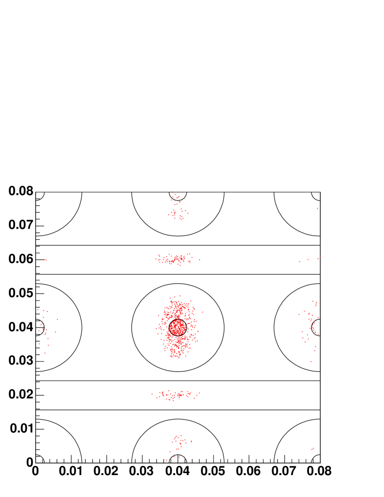
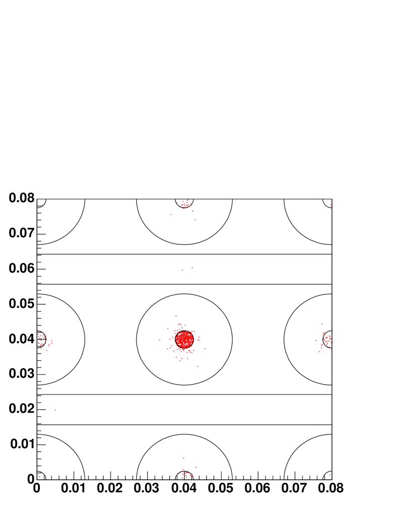
Figs. 5 and 6 show the electron drift lines and the distribution of terminal points of the drift electrons, where the results of the thin () and thick () substrates are shown in (a)s and (b)s, respectively. For , some of the drift lines end at the substrate (Fig. 5 (a)) and the resultant electrons are terminated on the substrate (Fig. 6 (a)). It was obvious that the buried anode readout buses distorted the drift electric field for , because the electron end points are distributed above the anode strips which are placed orthogonally to the cathode strips. On the other hand, most electrons are collected to the anode electrodes for . Fig. 7 shows dependence on . In the case of a thin () substrate, was found to be less than 0.5, while that with a thick () substrate exceeds 0.8. These results indicate that the -PIC with thick substrate already has a structure close to the optimal one in the view point of dependence on the substrate thickness.
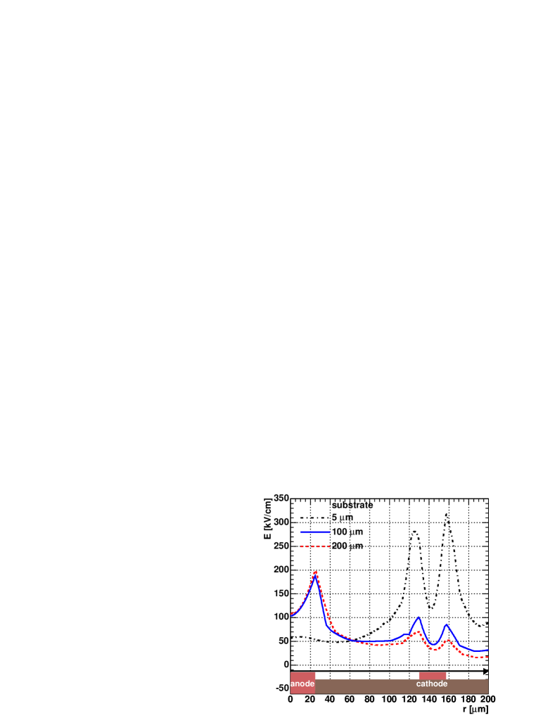
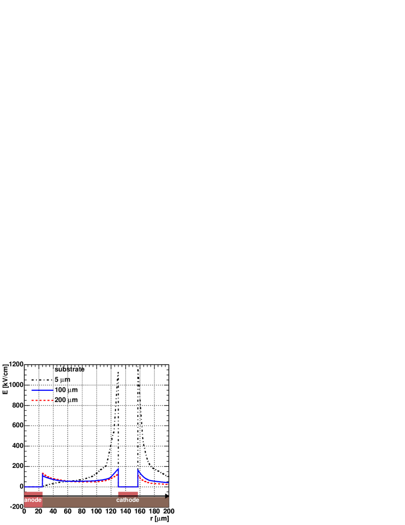
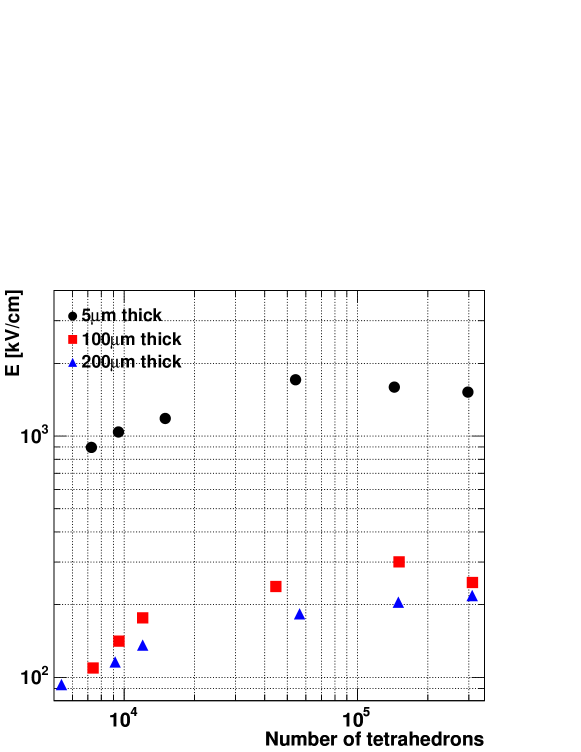
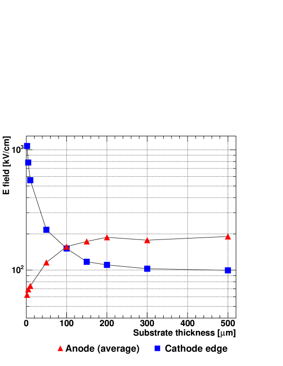
Another parameter which determines is . Because strongly depends on the electric field around the anode electrodes, also depends on . Fig. 8 (a) shows the electric fields as a function of the distance from the anode center at ( above the top of an anode). With a thin () substrate, the electric field averaged over the top area of the anode electrodes (hereafter ) reaches only 60kV/cm, while that with a thick () substrate exceeds 150kV/cm. For a thin substrate, the electron drift is affected by the rear side anode strip. Then large fraction of the drift electrons are not focused on the anode pixels. On the other hand, the electrode structure is similar to a wire chamber for a thick substrate. Most electrons are directed toward the anode pixels and collected on the anode. Thus a large is attainable for a thicker substate. The electric fields near the surface of the substrate () are also shown in Fig. 8 (b) as a function of , where the axis is located above the substrate. The electric field averaged along the circumference of the cathode ring (hereafter ) is found to be 10 times stronger for a thin () substrate than that for a thick () substrate. When we discuss the electric field around sharp points such as the cathode edge, the accuracy of the simulation has to be carefully considered. The detector structure and drift space consist of fine tetrahedrons in the FEM calculation. Then the number of tetrahedrons may represents the accuracy of the calculation. In this simulation, a unit cell includes 12000-16000 tetrahedrons. The mesh size is several which is smaller enough than the anode diameter. Since this does not seem to be very large for precise calculation, the validity of this accuracy was checked as follows. The electric fields at the cathode edge for several substrate thickness were calculated as functions of the number of tetrahedrons in the unit cell (Fig. 9). While the mesh size is relatively large (), the electric field at the cathode edge gradually increases as the number of tetrahedrons. For the larger number of tetrahedrons (), the resultant electric fields reach their plateau and can be regarded as constant within the error of 15% in RMS. Thus we used the = 12000-16000, which are reasonable numbers to save the CPU time.
The Townsend coefficient for a thin substrate becomes larger near the cathode edge, which is likely to cause discharges due to the emission of electrons from the cathode electrode. This is because the distance between the cathode edge and the anode readout bus () is much shorter than the distance between the anode pillar and the cathode edge (). On the other hand, if is larger than , the effect of the readout bus is efficiently shielded by the substrate, and the was weaker than the . and for various values are shown in Fig. 10. It is intuitively expected that should be at least weaker than , and the mechanism of discharges will be discussed in later section. Because is comparable to with , thickness of the substrate of the present -PIC is thought to satisfy the minimum point, though it is not still sufficient. Thicker substrate () would help to realize larger with the -PIC.
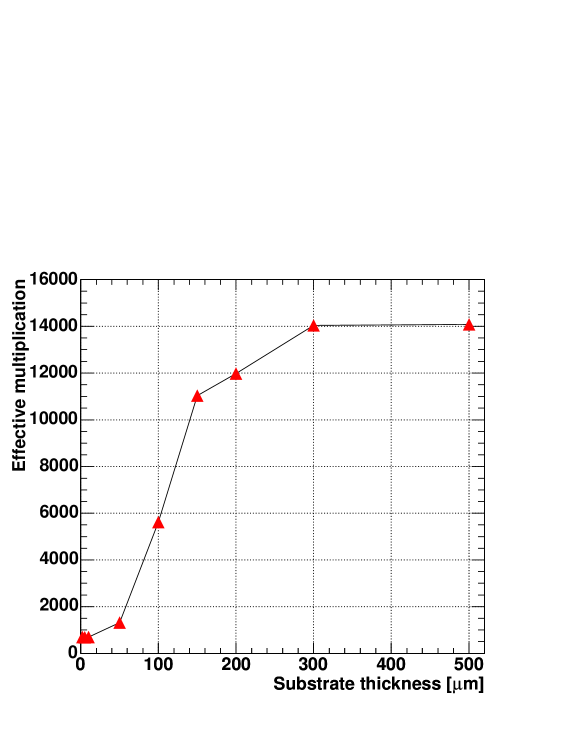
As the consequence of these two studies, thicker substrate is thought to bring larger . Fig. 11 shows as a function of . With a substrate thicker than , is expected to be twice larger than the current -PIC.
3.2 dependence on the anode diameter
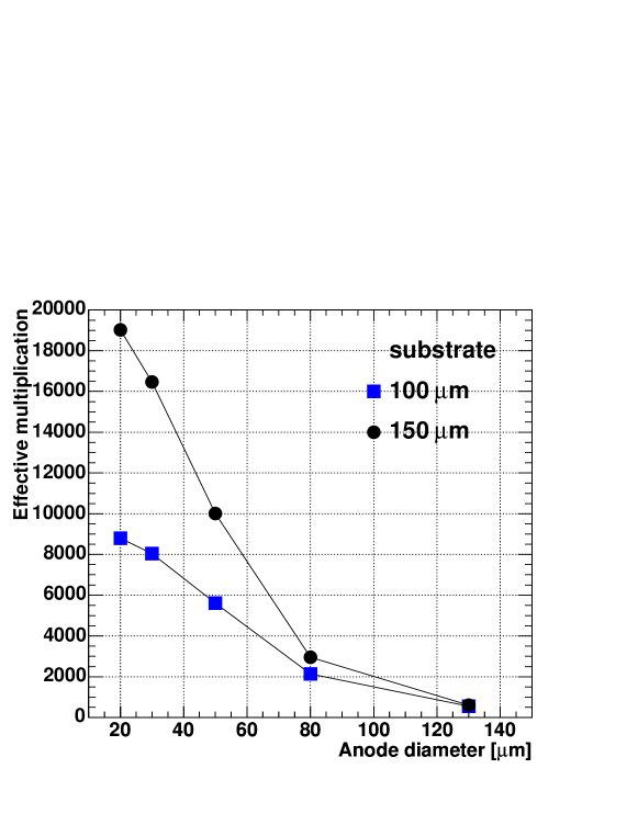
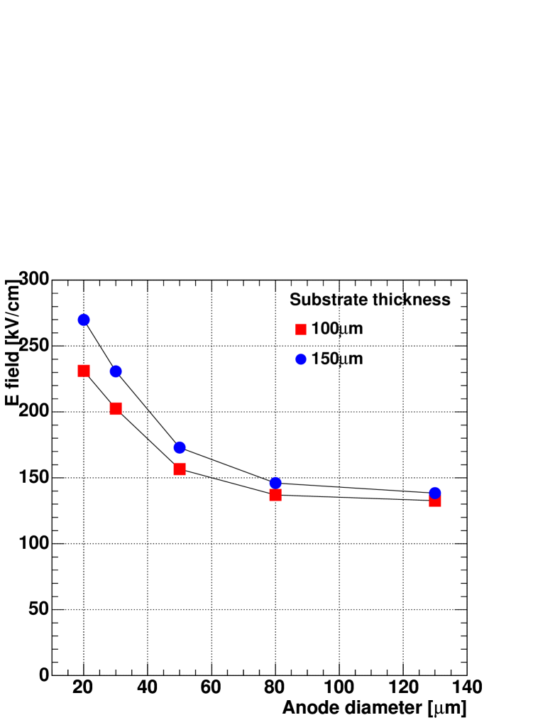
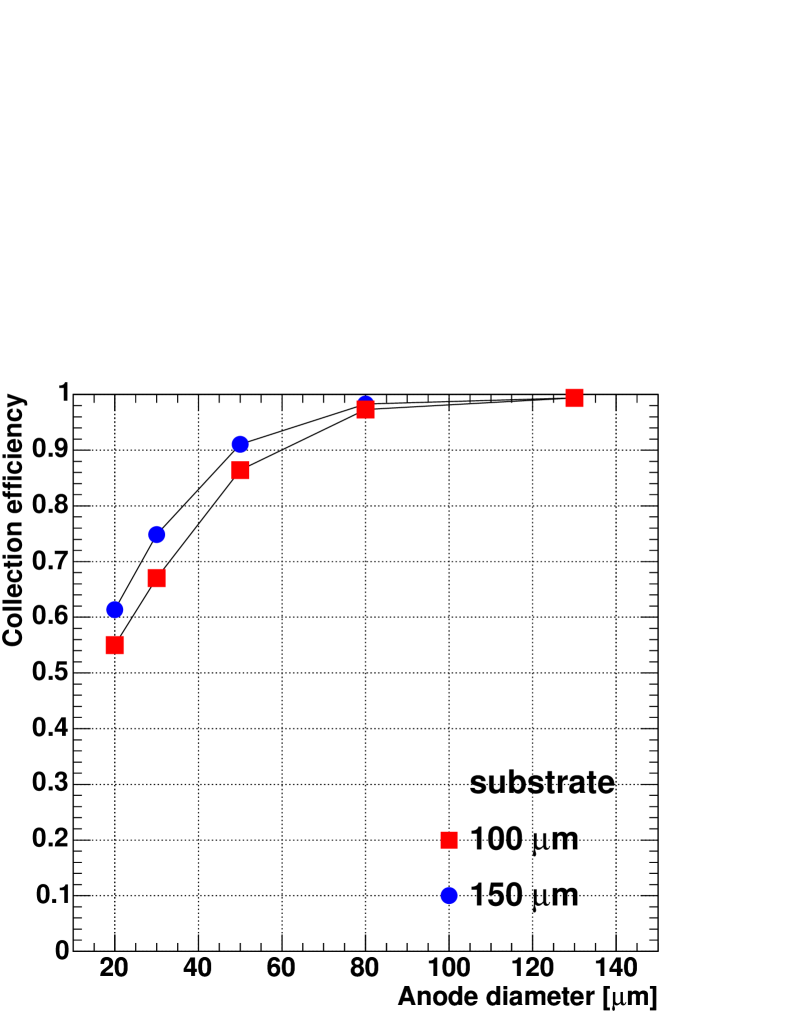
The dependences of the and on the anode diameter () were also studied. Although the current PCB technology can not manufacture an anode electrode with a diameter of smaller than for a thick substrate, it is worth investigating the optimum diameter. In this simulation, the anode diameter was varied from to and the electron drift and multiplication were calculated. Fig. 12 (a) shows as a function of . Obviously, decreases with increasing . On the other hand, large is expected for the large , as shown in Fig. 12 (b). Fig. 13 shows the effective multiplication factor as a function of . As is well known, this result shows that a smaller 20-30 has a larger gain; however, it also indicates that a sufficient multiplication is expected for an .
4 Detector optimization
In the previous section, we showed quantitatively that a thick substrate and a small diameter the of anode electrode would help to improve the performance of the -PIC. Because a smaller anode electrode is technically unreachable in the current -PIC fabrication method, we discuss the maximum of the -PIC with a thick substrate considering the maximum anode voltage for stable operation for a anode.
As indicated in earlier works about MSGCs [13, 14, 15, 16], one of the dominant mechanism of discharges in micropattern gas detectors is a consequence of the ejection of electrons from the cathode edge by spontaneous field emission. At a normal operation condition of MSGCs, the electric field near the cathode edge exceeds 100kV/cm, which is high enough for gas avalanche [15]. Therefore, electrons released from the cathode electrodes undergo the gas multiplication near both the cathode and anode electrodes, while the primary electrons have gas multiplication only near the anode electrode. We can assume that the electric field near the cathode governs the discharge process and “stable operation” can be judged by the cathode field. It is natural to think this discharge mechanism can be applied to -PIC and we can determine the maximum anode voltage by . As a result, the maximum is determined by .
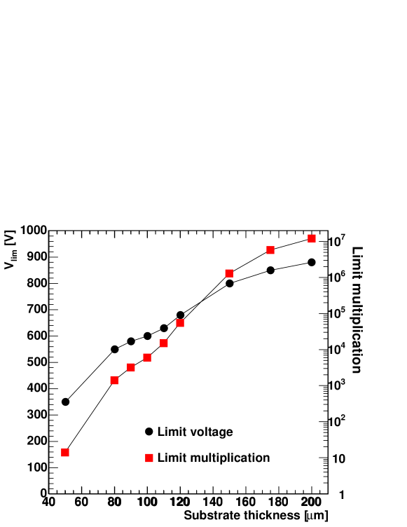
From the experimental results [3], we knew that the maximum allowable anode voltage was about 630V for (80/20) gas mixture, which corresponds to the maximum of 200kV/cm. We use 200kV/cm as the limit of . As mentioned in the previous sections, becomes weaker for a thicker substrate with the same anode voltage. In other words, the corresponding allowable voltage becomes higher for a larger . In Fig. 14, and corresponding are shown as functions of the substrate thickness. For a thicker substrate of , maximum anode voltage exceeds 800V, which the maximum gas multiplication for that voltage is higher than , as shown in Fig. 14. Taking into account the other factors, such as the non-uniformity of the shape of electrode, the gas gain might achieve for a thick substrate.
5 Summary
A three-dimensional simulation of the electron drift and gas multiplication in a -PIC was performed for optimizing the electrode structure using Maxwell 3-D field simulator and Garfield software. We found that the substrate thickness is a key factor for achieving both a high gas gain and stable operation. The electron collection efficiency and the gas multiplication factor became higher for a thicker substrate. In order to obtain sufficient gas gain for detecting minimum ionization particles, the substrate thickness of more than is required. Furthermore, a thick substrate also has an advantage for discharge suppression. The electric field near the cathode edge is weaker for a thicker substrate. The dependence of gas multiplication on the anode diameter was also simulated.
We estimated a limit voltage as a function of the substrate thickness based on experimental data, and found that would reach 800V when thickness is . In addition, a quite high gas gain of would be possible. We aim to achieve a thickness of in the next improvement of the -PIC.
Acknowledgments
This work is supported by a Grant-in-Aid for the 21st Century COE “Center for Diversity and Universality in Physics”, and a Grant-in-Aid in Scientific Research of the Japan Ministry of Education, Culture, Science, Sports and Technology, and “Ground Research Announcement for Space Utilization” promoted by Japan Space Forum. Also this work is partially supported by JAERI and KEK. T. N., R. O., and M. U. acknowledge the receipt of JSPS Research Fellowship.
References
- [1] A. Ochi et al., Nucl. Instr. and Meth. A 471 (2001) 264.
- [2] T. Nagayoshi et al., Nucl. Instr. and Meth. A 513 (2003) 277.
- [3] K. Miuchi et al., IEEE Trans. Nucl. Sci. 50 (2003) 825.
- [4] A. Takeda et al., to appear in IEEE Trans. Nucl. Sci.
- [5] S. F. Biagi et al., Nucl. Instr. and Meth. A 361 (1995) 72.
- [6] S. F. Biagi et al., Nucl. Instr. and Meth. A 392 (1997) 131.
- [7] T. Nagayoshi et al., Nucl. Instr. and Meth. A 525 (2004) 20.
- [8] M. Bouianov et al., “Performance optimisation of the Micro Pixel Chamber”, to appear in Nucl. Instr. and Meth. A.
- [9] Maxwell 3D Field Simulator, Ansoft Corporation, http://www.ansoft.com
- [10] R. Veenhof, Nucl. Instr. and Meth. A 419 (1998) 726.
- [11] S. F. Biagi, Magboltz, program to compute gas transport parameters, Version 2.2, CERN
- [12] S. H. Han et al., IEEE Trans. Nucl. Sci. 47 (2000) 1416.
- [13] T. Nagae et al., Nucl. Instr. Meth. A 323 (1992) 236.
- [14] Yu. N. Pestov et al., Nucl. Instr. Meth. A 338 (1994) 368.
- [15] T. Beckers et al., Nucl. Instr. Meth. A 346 (1994) 95.
- [16] A. Oed, Nucl. Instr. Meth. A 471 (2001) 109.
(a)
(b)

(a)

(b)
(a)
(b)
(a)
(b)
(a)
(b)