The BTeV RICH Front End Electronics
Abstract
We report on the design and testing of novel mixed analog and digital front end ASICs custom made for the single photon detectors considered for the BTeV RICH system. The key features are reviewed, as well as results achieved using electronics bench tests and beam studies.
keywords:
BTeV \sepFront End Electronics \sepPhotodetectors \PACS85.40.-e \sep85.60 Gz \sep85.60 Bt \sep07.07dfon behalf of the BTeV RICH Group
1 Introduction
Charged particle identification is a crucial component of any modern experiment studying charm and beauty decays. Ring Imaging Cherenkov (RICH) detectors offer a very attractive approach. The BTeV RICH detector has the important functions of separating , and also discriminating electrons and muons from pions.
The BTeV RICH detector is designed to separate in a momentum range of 3 to 70 GeV/ [1]. It is essential to CP violation studies, providing separation of specific final states, such as from , and also providing information on the flavor by identifying charged kaons. The RICH detector also complements the electromagnetic calorimeter and the muon detector in lepton identification and thus it increases the reconstruction efficiency in interesting modes like significantly. We use a novel gas radiator ( 111 is produced by 3M, USA, http://www.3m.com/ to generate Cherenkov light in the optical frequency range. The light is focused by mirrors onto two photon detector arrays. The two photon detector options that we considered were hybrid photo-diodes (HPDs), fabricated at DEP, the Netherlands 222Delft Electronic Products B.V. (DEP), http://www.dep.nl/ , and multi-anode photomultiplier tubes (MaPMTs), fabricated by Hamamatsu333Hamamatsu Photonics, Japan; http://usa.hamamatsu.com/, Japan. To separate kaons from protons below the threshold of gaseous radiator, a liquid radiator () is used and the light, proximity focused onto the sides of the vessel, is detected by 3” PMT arrays.
The design of these devices poses interesting challenges. Different tradeoffs between dynamic range and low intrinsic noise play a role in achieving optimal performance. Timing requirements are equally important, as we need to store the time-stamped event information in local buffers prior to the next collision, assumed to occur within 132 ns. Finally, although the RICH detector has generally very low occupancy, some areas experience high rates and we required these devices to be able to sustain the maximum rate, expected to be on the order of 3 MHz.
Two different custom made ASICs were designed and produced for us by IDEAS, Norway 444Ideas ASA, Ideas ASA, N-1330 Fornebu, Norway; http://www.ideas.no. The most extensive tests were performed on the VA_MaPMT circuit, packaged in the hybrid devices used in the BTeV RICH beam test studies described in another contribution to this conference [2].
2 Conceptual design of the VA_MaPMT ASICs
The detector segmentation chosen for our system makes it natural to use a binary output, as the signal is expected to be contained within a single pixel cell and the occupancy is very low so that it is very unlikely that a pixel is hit by more than 1 photon within any given event. This choice minimizes the number of bits of the hit information to be transferred. Finally, as the data needs to be collected in real time, the front end electronics includes self-triggering capabilities.
The specifications of the analog processor are different for the two photon detectors. The hybrid photon detectors (HPDs) pose the most stringent requirements on the intrinsic and common mode noise of the readout system. The expected charge signal distribution has a narrow width centered at about 5,000 ; thus the equivalent noise charge (ENC) of the electronics processor should not exceed 500 . Moreover, as the front end electronics incorporates a built-in discriminator, common mode noise must be negligible. This is a significant challenge for a device with distributed readout electronics and a 20 KV high voltage system. On the other hand, the MaPMT tubes feature an average gain in excess of 106. Even though the single photon response in this case is rather broad, the noise requirements can be relaxed, but high dynamic range becomes a critical feature.
These devices feature 64 parallel inputs and 64 parallel outputs. The parallel output architecture allows a prompt extraction of the channel hit information and the peripheral electronics can attach a time stamp to each event. The slow control is implemented as a serial bitstream that programs the mode of operation of the ASIC and allows the fine tuning of the individual channel thresholds described below.
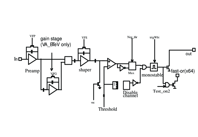
Fig. 1 shows the conceptual diagram of each readout channel. The analog section comprises a semi-Gaussian preamplifier and shaper circuit, followed by a high pass filter that reduces the discriminator sensitivity to long range drifts of the DC working point of the device. In addition, a voltage-controlled pole-zero cancellation circuit is introduced to optimize the rate capabilities.
The input of the digital section is a discriminator that must operate effectively at very low thresholds and it needs to tolerate very high rates, of the order of several MHz, to cope with the high occupancy expected in some areas. The discriminator threshold is set through an external 8 bit DAC. In addition, a 4 bit programmable DAC is built in every channel to fine tune the threshold of each individual channel to compensate for different DC offsets. The discriminator output drives a monostable circuit that produces an output current pulse whose width is about 100 ns. Individual digital outputs can be disabled through a channel mask set during the initialization sequence.
There are three modes of operation for this ASIC: (1) an initialization sequence, when a bit pattern sequence is shifted in the ASIC to program the desired operating conditions; (2) a calibration mode, when channels selected in the initialization sequence respond to an input current pulse sent to the calibration input; (3) finally, in normal mode, all the working channels are activated and respond to charge signals collected at their inputs. In addition, a fast-OR of all the channel hits can be activated for monitoring or synchronization purposes.
3 The front end ASICs
We started our R& D work with the ASICs best matched to the HPD application (VA_BTeV). In order to operate the discriminator with threshold levels of the order of about 30 mV, the RC-CR shaper is complemented by an optional gain stage, which provides an additional 3-fold amplification. When proper shielding and grounding for this device was achieved, the expected ENC of 500 at about 10 pF input capacitance was achieved and we were able to see efficient response to our blue LED single photon source.
Our next project involved the development of an ASIC to be used in conjunction with the R8900-M16 MaPMT tubes. In this version (VA_MaPMT), we reduced the gain of the analog front end, but we focused the design primarily in maintaining the capability of operating at very low thresholds. The linear range of the analog front end extended to 220 fC, assumed to be adequate for this application. An interesting feature added to this design was an analog channel that can be used to monitor the analog front end response either to a calibration pulse or can be connected to a given MaPMT pixel. This control channel proved extremely valuable in understanding the performance of this system with different ASIC biasing conditions and MaPMT high voltages. The performance of these ASICs will be the focus of this paper, as they have been more extensively tested in a variety of conditions.
The devices described in this paper are implemented in the 0.8 m N-well CMOS AMS process. A new iteration has been implemented in the 0.35 m CMOS process and features an extended dynamic range for MaPMT applications.
4 The front end hybrids
The HPD application involved also a packaging challenge. The 163 pixel HPDs produced for us by DEP [dep] had the pixel output brought outside the HPD vacuum by a pin array. This arrangement did not leave much space for electronics components, thus we used a rigid-flex-rigid technology, shown in Fig. 2. The octagonal rigid section contains the VA_BTeV ASICs and their biasing circuits, while the digital back end, coordinating the data transfer from front end ASICs to the data acquisition system, is hosted on the bigger rectangular section. The two rigid elements were connected electrically by a flex circuit embedded in the two rigid planes, that allowed the positioning of the digital section at a right angle with respect to the photon array plane.
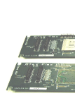
Fig. 3 shows the hybrid hosting the VA_MaPMT ASICs. It is a conventional 6-layer rigid printed circuit board. The analog inputs are routed via flat multiconductor cables to the base board hosting the MaPMT photon detectors and providing the high voltage biasing network for their 12 stages.
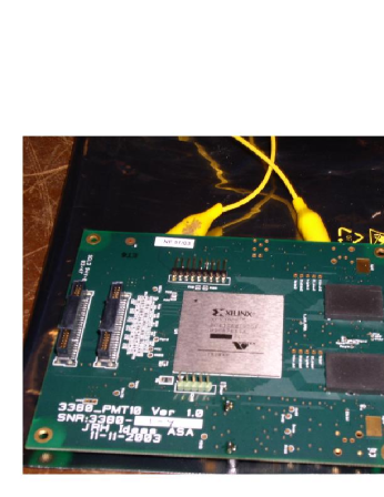
Both hybrids incorporate level shifter circuits that translate the current output from the front end ASICs into voltage level matching the input requirements of the XILINX Virtex 300 FPGA, used to drive the initialization sequence and to latch and transfer the data from the front end to the back end circuit with the protocols needed by the data acquisition system. The firmware can be downloaded in the first step of the initialization sequence and thus we could adapt this hybrid to different data taking modes, and different triggering configurations.
5 Performance
The initial set of measurements involved input charge scans at different threshold voltages. The shape of the transition between zero and maximal efficiency was used to estimate the intrinsic noise of the ASIC under test. From these measurements we inferred that a typical noise for the VA_BTeV mounted on the hybrid described above is about 500 , whereas the typical noise for the VA_MaPMT mounted on their custom made hybrids is about 2,000 .
The next tests involved the hybrids attached to their corresponding photon detector. The assembly was located in a test box where light from a blue LED was collimated onto a pixel of the photon detector. The LED was driven by a narrow pulse generator that biased the LED at tuneable very low light level. Both detector-electronics pairs demonstrated very good single photon sensitivity.
A set of ten MaPMT hybrids were used in a gas radiator RICH prototype that was taken to the test beam facility at Fermilab. Data were taken in two different periods, separated by a few months.
The results of the first set of data are discussed in a separate contribution to this conference [2]. We were able to operate at very low threshold throughout the duration of the data taking without additional noise hits. In particular, we were able to run with thresholds of 5 mV, corresponding to a minimum charge signal of 27,000 e-. With this threshold, the ratio between the input charge producing the onset of saturation and the minimum input signal to trigger the discriminator response is 52.
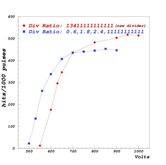
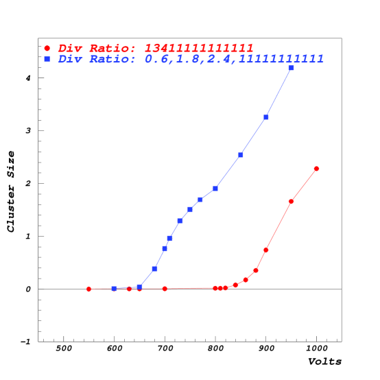
During the first run we observed unexpected cross talk between neighboring channels when the high voltages exceeded the onset of the plateau by about 50 to 100 V. Studies on the test channel with analog output connected to a MaPMT tube showed that the major cause of the cross talk was related to the analog channel going into saturation more and more frequently as the high voltage was increased above plateau. In order to reduce the gain without any collection efficiency loss at the first dynode, a different biasing condition for the MaPMT was suggested by Hamamatsu [3]. This new voltage divider ratio allows for the minimum voltage between the anode and the first dynode that is needed to achieve full collection efficiency at a lower value of the tube gain. The tradeoff between gain and crosstalk in the two configurations is shown in Fig. 4. The cross talk is characterized by the average number of hits recorded among the 6 closest neighbors to the channel attached to the MaPMT pixel: a value of 0 means that there is no cross talk, a value of 6 means that the neighboring channels are registering a hit whenever the MaPMT pixel is hit. The new biasing scheme represents an improvement, but the spread in gain between different tubes suggests that a more robust option is an increase in the linear dynamic range of the front end electronics. This option has been implemented in a new iteration of this ASIC, presently being characterized.
6 Conclusions
We successfully developed and characterized custom made ASICs to process the signal from HPD and MaPMT photon detectors for the BTeV RICH gas detector. Although the BTeV experiment was terminated by an executive budgetary decision, we envisage a variety of applications for these devices in high energy physics, astrophysics and medical applications.
7 Acknowledgements
I would like to acknowledge the conference organizers for an outstanding scientific program in an inspiring and charming setting. Many thanks are due to my colleagues of the BTeV RICH group: S. Blusk, C. Boulahouache, J. Butt, O. Dorjkhaidav, N. Menaa, R. Mountain, H. Muramatsu, R. Nandakumar, L. Redjimi, K. Randrianarivony, T. Skwarnicki, S. Stone, R. Sia, J. Wang, and H. Zhang. I would like to thank S. Mikkelsen and B. Sundal, and the other IDEAS engineers, whose electronics skills made this development possible. I would also like to thank my BTeV collaborators, for challenging discussions in the very productive years of this research and development. Finally, my warmest thanks are due to our spokespersons, J. Butler and S. Stone, whose dedication to the success of BTeV was a true inspiration. This work was supported by the US National Science Foundation.
References
- [1] The BTeV Collaboration, The BTeV Technical Design Report, Dec. 2004.
- [2] T. Skwarnicki, Contribution to these proceedings, 2005.
- [3] Y. Yoshizawa, private communication, Jun. 2004.