A 96-Channel FPGA-based Time-to-Digital Converter
Abstract
We describe an FPGA-based, 96-channel, time-to-digital converter (TDC) intended for use with the Central Outer Tracker (COT) COT in the CDF Experiment CDF_TDR at the Fermilab Tevatron. The COT system is digitized and read out by 315 TDC cards, each serving 96 wires of the chamber. The TDC is physically configured as a 9U VME card. The functionality is almost entirely programmed in firmware in two Altera Stratix FPGA’s. The special capabilities of this device are the availability of 840 MHz LVDS inputs, multiple phase-locked clock modules, and abundant memory. The TDC system operates with an input resolution of 1.2 ns, a minimum input pulse width of 4.8 ns and a minimum separation of 4.8 ns between pulses. Each input can accept up to 7 hits per collision. The time-to-digital conversion is done by first sampling each of the 96 inputs in 1.2-ns bins and filling a circular memory; the memory addresses of logical transitions (edges) in the input data are then translated into the time of arrival and width of the COT pulses. Memory pipelines with a depth of 5.5 s allow deadtime-less operation in the first-level trigger; the data are multiple-buffered to diminish deadtime in the second-level trigger. The complete process of edge-detection and filling of buffers for readout takes 12 s. The TDC VME interface allows a 64-bit Chain Block Transfer of multiple boards in a crate with transfer-rates up to 47 Mbytes/sec. The TDC also contains a separately-programmed data path that produces prompt trigger data every Tevatron crossing. The trigger bits are clocked onto the P3 VME backplane connector with a 22-ns clock for transmission to the trigger. The full TDC design and multi-card test results are described. The physical simplicity ensures low-maintenance; the functionality being in firmware allows reprogramming for other applications.
I Introduction
The Collider Detector at Fermilab (CDF), is a large (5000-ton) detector of particles produced in proton-antiproton collisions at 1.96 TeV at the Fermilab Tevatron CDF_TDR . The detector consists of a solenoidal magnetic spectrometer surrounded by systems of segmented calorimeters and muon chambers. Inside the solenoid, precision tracking systems measure the trajectories of particles; the particle momenta are measured from the curvature in the magnetic field and the energy deposited in the calorimeters. The tracking systems consist of a silicon-strip system with 750,000 channels around the beam-pipe, followed by the Central Outer Tracker (COT), a large cylindrical drift chamber with 30,240 sense wires arranged in 96 layers divided into 8 “superlayers” of 12 wires each COT . Four of the layers have the wires parallel to the beam axis; the remaining four are tilted by degrees to provide small-angle stereo for 3D reconstruction of tracks. The maximum drift time of the COT is 200 ns; the maximum drift length is 0.88 cm.
During the present Run II, which started in 2001, the peak luminosity of the Tevatron has grown to over cm-2sec-1, a factor of more than five higher than in Run I. The Tevatron operates with a bunch spacing of 396 ns, with the result that the occupancy (hits/channel) in the COT increases with luminosity as the average number of proton-antiproton collisions per bunch crossing is now substantially greater than one. The increased occupancy will decrease the rate at which CDF can record events to permanent media. In addition, although CDF is presently operating at its design readout bandwidth, there are still more events of physics interest than can presently be logged, particularly due to the success of the Silicon Vertex Trigger (SVT), which has given CDF an expanded capability to trigger on events from b-quarks. A broad range of efforts are underway to upgrade the readout bandwidth to allow operation at luminosities up to cm-2sec-1, including the development of a new time-to-digital converter (TDC) for the COT.
In this note we describe the design of a new TDC for the COT based entirely on field-programmable gate arrays (FPGA’s). Thirty working prototypes have been built and tested. A comprehensive suite of test routines, including some that exploit the capabilities of large FPGA’s to implement sources of test data, has been implemented and documented. We present results on performance and readout bandwidth.
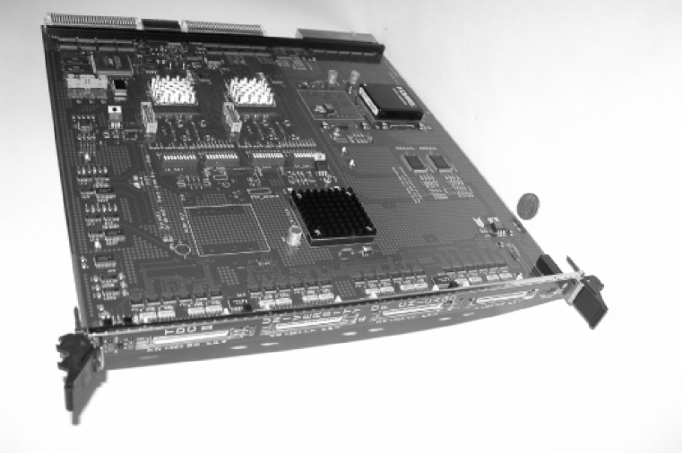
The use of large FPGA’s allows a board layout with very few chips, as all of the data-processing functions of the TDC are contained in the two FPGA’s, each of which handles 48 channels. A third, smaller, FPGA serves as the VME interface. The other chips on the board are delay lines, buffers on the input and output signals to the connectors, and DC-to-DC converters to supply voltages not available in the existing VME ANSIVIPA ; CDFVME crates. The exceptionally low chip count, few internal connections, all digital-nature, and extensive diagnostic capabilities make the boards easy to test and maintain. Figure 1 shows one of the 30 preproduction boards.
II TDC Specifications
A summary of the TDC physical and operational characteristics is given in Table LABEL:table:specs. The schematics of the board are available at Schematics . Details of how the TDC operates are given in the text below.
| Characteristic | Values | Comment |
|---|---|---|
| TDC Digitization Performance | ||
| Channels | 96 | 48/FPGA |
| Time Bin Size | 1.2 ns | |
| Hits/Channel | 7 hits | Configurable via VME |
| Min Time Between Hits | 4.8 ns | |
| Full Scale Range | 304.8 ns | 254 1.2 ns |
| Min Width/hit | 4.8 ns | |
| Max Width/Hit | 304.8 ns | |
| Non-Linearity | counts | count typ. nonlinearity |
| L1 Pipe-Line Size | 512 words/6.144 s | 480-bit words |
| Test Data RAM size | 512 words/6.144 s | 480-bit words |
| L2 Buffer Length | 64 words/768 ns | 480-bit words; Configurable |
| Processing Time | 12s after L2A | Includes readout packing |
| Min interval between L2A’s | 12 s | L2A is Level-2 Accept |
| Prompt (Trigger) Outputs | ||
| XFT Trigger bits/wire | 6 | From 11 time windows |
| XFT Time-window | 6 ns | Min 1.2 ns; Max 12 ns |
| # of XFT Time-windows | 11/wire | Mapped into 6 trigger bits |
| Trigger Latency | 80 ns after BC | First word out |
| Trigger Output freq. | 32 bits/ 22 ns | See Fig. 12 |
| Trigger Output | 43 pins | TTL, on VME P3 |
| Readout Characteristics | ||
| VME Interface | VME64 | Implemented in FPGA |
| VME Readout Modes | A32/D32, A32/D64 | D64 in CBLT mode only |
| CBLT64 Transfer Rate | 47 MBytes/s | Burst speed |
| Test Modes | Data Generator | Internal 8192 word memory |
| Physical Characteristics | ||
| Physical Format | 9U VME | ANSI VIPA ANSIVIPA |
| Power Requirements (V/A) | +5V/15A; -5V/2A | |
| Input Connectors | 68-pin | Mini-D Ribbon |
| Input Levels | LVDS | CDF uses quasi-LVDS QuasiLVDS |
| Front Panel LEDs | 1 Triple LED/FPGA | Configurable in firmware |
| Trigger Output Connector | VME P3 | |
III Principle of Operation
Secondary particles from antiproton-proton () collisions traverse the Tevatron beam pipe, the silicon-strip vertex detector, and then the COT drift chamber volume. The charged particles ionize the gas in the drift chamber volume; the tracks are measured from the time of arrival of the ionization on the sense wires of the COT COT . These electrical pulses, colloquially known as ‘hits’, are amplified and shaped by the Amplifier Shaper Discriminator (ASDQ) cards COT directly on the end-plates of the COT, and transmitted to ‘Repeater cards’ that drive the cables to the VME crates on the outside of the magnet yoke that contain the TDC boards. The TDC is used to digitize the time of arrival and, as a measure of pulse height, the width of the pulses from the Repeater cards.
The Time-to-Digital conversion is implemented with two Altera Stratix FPGA’s, each handling 48 sense wires. This device has an LVDS differential I/O interface that consists of one dedicated serializer/deserializer circuit Stratix for each of the 48 differential I/O pairs. Serial data are received along with a low-frequency clock. An internal phase-locked loop (PLL) multiplies the incoming clock by a factor of 1 to 10. Each input signal is sampled at the resulting high-frequency clock rate, converting it to a (1-bit) serial stream, which is then shifted serially through a shift register. The shift register is read out as a parallel word at the low frequency clock rate, thus converting the serial data stream into a parallel data stream that contains the input data sampled at the higher clock rate. In this application the low-frequency clock is internally generated with a 12 ns period and the multiplier factor is set to 10, for a resulting 1.2 ns sampling rate of the incoming LVDS signal and a 10-bit wide parallel data stream.
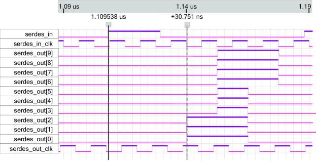
Figure 2 illustrates the serial-to-parallel conversion, as seen in the Altera Quartus II Quartus simulation window. The input pulse is converted into a 10-bit parallel data stream, (labeled as serdes_out[9..0] in the figure) clocked at a 12 ns period. The leading edge of a ‘hit’ in the tracking chamber is then determined in the Edge Detector Block by counting the number of “0” bits before the first “1” bit of a string of at least four “1” bits in 2 consecutive words at a time. The width of a hit is calculated by counting the number of successive bits (either 0 or 1) until the start of a string of at least four consecutive “0” bits occurs.
IV TDC Board - Block diagram
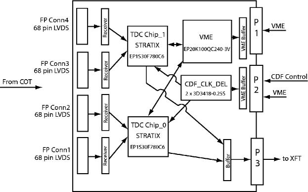
The physical layout and the data flow on the board are presented in Figure 3. We step through each element in turn below.
-
•
The Front Panel (on the left in Figure 3) receives 96 differential inputs, arranged in four 24- channel connectors, which receive pulses from the amplifier/shaper circuits of the COT. The signals are first applied to a receiver block that converts them from a CDF-specific quasi-LVDS signal QuasiLVDS into standard LVDS and passes 48 of them directly to each of the two FPGA TDC chips, which have identical designs.
-
•
Each of the two TDC FPGA’s (TDC Chip’s) does the time-to-digital conversion for 48 wires to generate the Hit- Count and Hit-Data results. These are stored in internal VME Readout buffers implemented on the chip. The TDC Chips also generate prompt data for the Level-1 track trigger processor (XFT).
-
•
The VME interface block is implemented with an Altera Apex FPGA Altera_Apex . The block coordinates VME access to the TDC Chips for regular and Chain Block Transfers (CBLT) ANSIVIPA in both 32-bit and 64-bit modes. The VME chip itself is connected to only the 16 least significant bits of the VME data bus (the TDC Chips connect to all 32 data lines).
-
•
Control signals from the CDF data acquisition and trigger systems are brought onto the TDC board using user-defined pins of the VME P2 backplane connector. The control signals are bussed on the backplane of the CDF-standard 9U VME/VIPA crate ANSIVIPA ; CDFVME from a CDF Tracer Card Tracer to each of the TDC boards. The specific control signals used by the TDC are as follows:
-
–
The CDF system clock - this is the master reference signal for the CDF data-acquisition system. The clock has a 132-ns period and is synchronous with the accelerator RF structure. On the TDC board the differential PECL signal from the backplane is first converted to TTL, then phase-locked, buffered and applied to the TDC chips. The clock signal is also applied to the TDC chips after passing through a pair of programmable delay lines (0.25ns granularity, 64ns range).
-
–
The Bunch Crossing signal (BC), indicating that a clock corresponds to a crossing of proton and antiproton bunches.
-
–
The Bunch 0 signal (B0) marks the first proton bunch which comes once per cycle around the Tevatron ring.
-
–
The Level l and 2 trigger Accept/Reject signals, as well as the Level 2 Buffer address bits.
-
–
The CDF_TDC_CALIB pulse from the VME backplane. This is converted from PECL to ECL and can be applied to a pair of pins on each of the four front panel connectors. The pulse is thus sent to the amplifier-discriminator-shaper card (ASDQ) of the COT[1] and is used for testing and calibration.
-
–
-
•
The VME P3 backplane connector is used to transmit trigger flags generated by the TDC to the eXtremely Fast Tracker (XFT) processor to identify tracks in the COT for the Level-1 trigger.
-
•
Each FPGA is connected to a 20-pin header so that it is easy to use a logic analyzer for testing and diagnosis. Signals can be routed to the header by programming the FPGA firmware.
V The TDC FPGA Chip
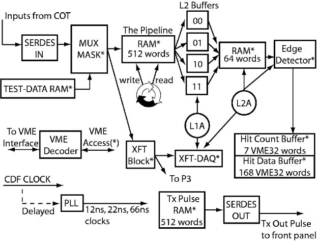
The block diagram of a TDC Chip is presented in Figure 4. There are two major data paths inside the TDC Chip, one to record the COT hits for VME readout, and one for the generation of the prompt trigger bits (‘Trigger Primitives’) for the XFT trigger track processor. The Chip is also provided with a Test Data generator, an LVDS pulse generator and a PLL clock generator.
The major functional blocks inside the TDC Chip are described individually below. These are implemented as firmware and are optimized for the CDF application; other applications can be accommodated by firmware changes.
V.1 The Input Block
Each TDC Chip has four banks of 12 high-speed LVDS inputs. From each bank a 120-bit wide data bus passes data to the MUX/MASK block (see Fig. 4), which can be set under VME control to block out any unwanted channel (for example, a COT wire that is continuously set true due to a some failure). The MUX/MASK block also allows internal testing of the TDC Chip by allowing the inputs to be switched to a test pattern generated inside the Chip with the Test Data Generator block (described in Section V.5). The fast digitization and conversion to a 10-bit wide data stream for each channel then follows.
V.2 The Pipeline and The Level 2 Buffer System
The CDF Level-1 trigger is deadtime-less, with all front-end data held in a pipeline for 5.544 s while the Level-1 trigger decision is being made CDFtrigger . On the TDC card the delay is implemented with a clocked pipeline. On receipt of a BC signal, an input memory address counter is set to zero; the counter then increments on every 12 ns clock. The phase of this input pulse can be adjusted at each board to compensate for signal propagation and input signal length differences adjust_phase . The memory is 512 words deep, each word containing 480 bits (48 channels 10 bits/channel). The memory has two ports; the first port is always writing and the second port is always reading. The adjustable address of the second port, an offset from the first port, is set to establish the desired delay period for the pipeline. The maximum delay is 6.1s.
To reduce deadtime in the CDF Level-2 (L2) trigger system, on a Level-1 Accept signal (L1A) the data from a given beam crossing are transferred to one of four Level-2 buffers, awaiting a L2 trigger decision CDFtrigger . The four L2 buffers are independently controlled by an accompanying L2 buffer-selection signal. These signals are in phase with the CDF clock pulse. The L2 buffers are two-port memories; each has a respective write address counter for the input write port and all share a single address counter for their (output) read port. This allows the writing of a second Level-1 buffer while a first is still collecting data. The write clock is synchronous with the logic in the pipeline, 12 ns per tick. The data are written 10-bits-wide per channel, so that 48 channels are written at each tick in a 480-bit wide word. To achieve a maximum of 384 ns for the time range, the maximum length is 32 words, set via VME at initialization (the maximum drift time in the CDF COT is 200 ns).
A Level-2 Accept signal, together with an address pointer, selects one of the four Level-2 buffers to be transferred to the Edge Detector Block. The read port of the selected memory is driven through the full range of stored data addresses to present all the stored data. As not all buffers contain data from beam crossings that pass the Level-2 trigger (and therefore these would not receive a Level-2 Accept signal), the logic allows any Level-2 buffer to be overwritten whether or not it has been read. No data memory buffer is ever erased.
V.3 The Edge Detector Block
The purpose of the Edge Detector Block is to find hits on the wires. Hits are defined as pulses of at least 4.8ns in width. Since the pulses can be of indefinite length, the techniques of pattern matching or look-up tables cannot be used. The technique used in the Edge Detector Block is to look for leading and trailing edges of a pulse. A leading edge is defined as a transition from low (0) to high (1) and a trailing edge is defined as a transition from high (1) to low (0). It is assumed that all wires start out in a low (0) state and the first transition to find is a leading edge.
The Edge Detector Block is made up of two modules. The first, called the ED, finds and stores the edges on each of the 48 wires. The second, called the ED48, controls the timing of the data transfer into the Edge Detector Block, collects and packs the output hit data, and signals when the Block is finished. Each wire has its own dedicated ED module, making 48 on each TDC Chip; there is only one ED48 module on each Chip.
The data from the Level-2 Buffer are fed into the Edge Detector Block in 10- bit words. A single ED looks for hits in two consecutive 10-bit words at a time. The beginning of a hit is defined as a zero followed by at least four ones, or in the case of the first word, four ones in a row ED_startup . The end of a hit is defined as a one followed by four zeroes. There are three possible transitions in each word and each transition needs a memory cycle.
V.3.1 A Worked Example
Table 2 shows the relationship between the position of bits in the words sent to the ED and their respective time value as an example in a word that has three possible transitions.
| Bit Position | [9] | [8] | [7] | [6] | [5] | [4] | [3] | [2] | [1] | [0] |
|---|---|---|---|---|---|---|---|---|---|---|
| Sample data | 0 | 1 | 1 | 1 | 1 | 0 | 0 | 0 | 0 | 1 |
| Time value | 0 | 1 | 2 | 3 | 4 | 5 | 6 | 7 | 8 | 9 |
In this case, there is a leading edge (transition #1) starting at time value 1 and ending at time value 4 (transition #2). There is also possibly another leading edge (transition #3), starting at time value 9, depending on what is in the next word. In this case, the ED, which looks at 2 words at a time, would find a hit if the next word started with three ones.
Once a hit has been found, the data describing the hit are stored and the hit total is incremented. Each ED has a RAM for storing the hit data. Each hit is characterized by the number of the time bin of the leading edge and the width, expressed as the number of time bins in the hit. Thus if the data in the example of Table 2 were the first word in the data stream, the leading edge stored would be 1 and the width would be 4. If instead the example data were the third word, the leading edge time would be 21 (10 bits each for the first and second words plus time value 1 in the third word) and the width would still be 4.
V.3.2 Maximum Number of Hits and Words
The maximum number of words looked at per beam crossing for each wire is variable, with a maximum of 33 words (396/12). The maximum is set by the time between Tevatron beam crossings, 396 ns, and the data clocking period of 12 ns for each word (1.2 ns per bit times 10 bits per word). The number of words to be searched by the ED is set in a register via VME at initialization.
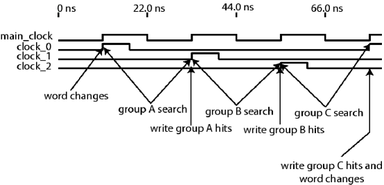
Since the possibility exists that a single word could have three transitions, the ED looks at each word three times, as shown in Figure 5. On a clock_0 signal, a new data word moves into a register in the ED called next_word. The word that was previously in register next_word is moved into a register called first_word. The ED tries to match the pattern ”01111” with first_word[9..5], first_word[8..4], first_word[7..3] or first_word[6..2]. These four register segments are known as group A. If the pattern matches, a flag signals that the next group should look for a trailing edge pattern ”10000”, otherwise the search for a leading edge continues. On a clock_1 signal, the pattern matching is repeated, but the register segments searched are the ones starting with bits 5-2. These segments are known as group B. On a clock_2 signal, the register segments searched are the ones starting at bits 1 and 0 and are known as group C. The possibility of a hit wrapping around the end of the data word is accounted for by using the some bits in the next_word buffer in groups B and C. On the next clock_0 signal, the new data word moves into next_word, the current next_word moves into first_word and the entire process is repeated until the last data word is moved out of first_word.
The maximum number of hits stored is 7. Each ED has two small RAMs that hold the leading edges and widths. These RAMs are called le_ram (‘le’ for ‘leading edge’) and width_ram; each can hold eight 8-bit words. Eight-bits limits the value of leading edges and widths to values 255 and less explain254 .
V.3.3 Clocks and the Edge Detector
There are four clocks used in the ED, as described in Table 3. Figure 5 graphically shows the clocks and the tasks performed during the different states.
| Clock Name | Clock Period | Phase | Duty Cycle |
|---|---|---|---|
| Main Clock | 22 ns | 0 ns | 50% |
| Clock_0 | 66 ns | 17.6 ns | 10% |
| Clock_1 | 66 ns | 39.6 ns | 10% |
| Clock_2 | 66 ns | 61.6 ns | 10% |
V.3.4 The Edge Detector 48 (ED48) Module
The second part of the Edge Detector block is the ED48 module. The ED48 takes the data from the small (8-bit8-word) RAM in each Edge Detector and packs the bytes into two larger RAMs. The number of hits found on each wire is held in the Hit Count RAM, configured in the FPGA as 32 bits7 words. The hit data are stored in the Hit Data RAM, configured as 32 bits168 words (see Table 4).
| Word | Bits 31.. 24 | Bits 23..16 | Bits 31.. 24, | Bits 23..16 |
|---|---|---|---|---|
| Leading edge | Width | Leading edge | Width | |
| Word 0 | Hit #1, Wire 1 | Hit #2, Wire 1 | ||
| Word 1 | Hit #1, Wire 2 | Hit #1, Wire 3 | ||
| … | … | … | ||
| Word N | Hit #k, Wire j | Hit #(1), Wire (j+1) | ||
| Word N+1 | Hit #2, Wire (j+1) | Hit #(3), Wire (j+1) | ||
| … | …. | |||
The Hit Count RAM stores the number of hits on each wire as 4 bits, so that each 32-bit word contains the hit count for 8 wires (See Table 5). The first six words store the information for the 48 wires per Chip. The last word is a header word that contains the bunch crossing counter, L2 buffer number, Chip serial number and module ID (See Table 6).
| Word | Bits | Bits | Bits | Bits | Bits | Bits | Bits | Bits |
| 31-28 | 27-24 | 23-20 | 19-16 | 15-12 | 11-8 | 7-4 | 3-0 | |
| 0 | Wire 7 | 6 | 5 | 4 | 3 | 2 | Wire 1 | Wire 0 |
| … | … | … | … | … | … | … | … | … |
| 5 | Wire 47 | 46 | 45 | 44 | 43 | 42 | Wire 41 | Wire 40 |
| 6 | Header Word | |||||||
| Bits | Description |
|---|---|
| Bunch Crossing Counter | |
| of hits in Hit Data block | |
| L2 Buffer Number | |
| Unused, always 0 | |
| Chip Serial Number: 0 for Chip 0 and 1 for Chip 1 | |
| TDC Type:() | |
| Module ID -set with a VME write CDF6998 |
A Level 2 Accept signal initiates the reading of data from the Level 2 Buffer by the ED48 ED_read . The ED48 module sends a signal to each ED to clear its buffers, and then sends a signal to the Level 2 Buffer module to start sending data. The signal TDC_DONE, which is available in a VME register, is set to false indicating that hit-processing is in progress. At this point, the ED48 does nothing until the 48 ED’s are finished working. The ED48 module then sums the word counts from each ED. This sum is the number of 16-bit words to be written in the Hit Data RAM. Since the data are taken out of the RAM on a 32-bit bus, the 16-bit word count is then divided by two to get the number of 32-bit words to be read.
To move the data quickly from the ED modules to the Hit Data RAM, the ED48 module is organized into four sections, each holding 12 Edge Detectors. Four 12-input multiplexers are used to stream the data from the small ED RAMs to the Hit Data RAM in the ED48. This allows data to be written on each clock cycle and requires only one extra clock cycle when changing EDs.
There are twelve 12-input and three 4-input multiplexers used to control the flow of data from the ED modules to the RAMs in the ED48. One 4-input and four of the 12-input multiplexers are used each for the leading edge data, the widths, and the word counts.
A combination of counters and multiplexers control the flow of data from the 8-word/8-bit RAMs in each ED to the Hit Data RAM in the ED48. The number of words read from each small RAM is constant and equal to the number of hits specified, and is independent of the number of hits found on a wire. If the number of hits to search for (set by VME) is specified as six, then six words will be read from the little RAM in each ED. At this point, the ED48 module uses the word count from each ED to determine when the write-enable signal on the Hit Data RAM should be turned on and off.
The write-enable signal is controlled by the output of a compare megafunction Stratix that compares the address sent to the 8-word/8-bit RAMs in the ED modules with the hit word count for the wire.
Once the ED48 is finished getting the data from each of the 48 ED modules, it sends a signal to clear all of the ED counters and flip-flops, and sets the signal TDC_DONE. This signals that the data are ready to be read out of the memories of the ED48 module via VME.
The ED48 module controls the word counts that are written to the Hit Data RAM with three signals, called save_wc, write_wc, and clear_wc. When the ED modules are finished, the hit count for each wire is written to the Hit Data RAM. The word counts are registered onto the bus to the Hit Count RAM one clock cycle after the EDs are done, and on the next clock cycle, are written to the RAM. When the ED48 module is finished, this bus is also cleared.
V.4 The XFT Block
The TDC XFT block generates ‘Trigger Primitives’ used by the eXtremely Fast Tracker (XFT) Nils_Krumnack , which identifies tracks in the Central Outer Tracker (COT). The tracks are used in the Level 1 Trigger, as well as in Level 2, and consequently the complete pattern recognition and momentum reconstruction have to be available within 5.5 s after the beam crossing. The sense-wire planes of each superlayer in the COT are tilted in the plane so that a high momentum track will traverse each superlayer COT , and consequently will travel between a pair of sense wires in each plane, resulting in some hits that are ‘prompt’. The present Run IIa XFT splits the 396-ns interval between beam crossings into three time bins, a prompt, a not sure, and a delayed time bin. These three bins are logically combined to give 2 trigger bits per wire every 396 ns. The new TDC/XFT design described here uses 11 time windows to produce 6 output trigger bits per COT wire every 396 ns. The 6 bits, referred to below as ‘Trigger Primitives’, are derived from the hit occupancies in the 11 time windows with Boolean logic. The larger number of time windows allows better momentum resolution and fake track rejection.
The Trigger Primitives, consisting of the 6 bits per wire times 48 wires, are output each 396 ns from the XFT block on each of the 2 FPGA’s. Every 22 ns the TDC Chip sends out 16 bits to the P3 backplane (48 bits for 66 ns, and so 48*6288 bits for 396 ns). In order to speed up the transmission of data to the XFT, the bit for each of the (up to 6) time bins is transmitted in turn after the calculation for its corresponding three time-windows (see below) is completed. The time windows can be reprogrammed to optimize performance by changing data in VME registers without firmware changes.
The TDC XFT block receives two types of signals:
-
•
CDF control pulses (Bunch 0 (B0), Bunch Crossing (BC));
-
•
The primary (digital) data-stream from the COT.
The XFT block sends out timing alignment signals and the Trigger Primitives (trigger bits) to the P3 connector on the VME backplane for transmission to the XFT. The TDC XFT block is controlled by two VME registers and an internal RAM CDF6998 . The values of the registers determine the input and output delays, and the RAM contents define the time-window intervals.
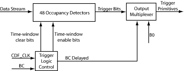
The TDC XFT block includes three main blocks (Figure 6):
-
•
Trigger Logic Control. This receives the B0 and BC pulses, and controls the other parts of the TDC XFT;
-
•
48 Occupancy Detectors. These receive the digitized COT data stream (480 bits/12 ns), perform hit recognition, and send out 6*48 Trigger Primitive bits for every bunch crossing to the Output Multiplexer;
-
•
Output Multiplexer. This receives the trigger bits from the 48 Occupancy Detectors and sends the Trigger Primitives in parallel to the P3 backplane in 16-bit words every 22 ns.
V.4.1 The XFT Occupancy Detector
Every 12 ns clock each Occupancy Detector (OD) receives a 10-bit data-stream word. Each OD looks for a “1111” pattern (a hit) in two consecutive words in the data stream (20-bits), which corresponds to a 24 ns time interval. The search for hits is performed separately by two Hit Scanners inside each OD; one for hits starting in the first 5 bits (6 ns), and the second for hits in the next 5 bits of the 20-bit data segment. Figure 7 shows the block diagram of the Hit Scanners in the Occupancy Detector. If a hit starts in the first 6 ns the signal labeled “major_e” is set high. Similarly, if a hit starts in the last 6 ns the signal labeled “major_l” is set high. The 10-bit bus labeled “store[9..0]” is an input data stream for a single wire; the signal labeled “Clock” is the 12 ns clock.
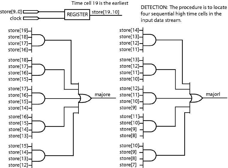
Each Occupancy Detector contains 11 independent registers (‘time-window registers’) that store hit information. Each register corresponds to a time-window. In the current firmware design each time-window is controlled by two bits (‘time-window control bits’), used to implement separate hit scanning for the first and the last 6 ns of each 12-ns clock interval. If the first bit is high, the register is sensitive to hits started in the first 6 ns of every 12 ns (first 5 bits of 10-bit data word). Similarly, if the second bit is high, the register is sensitive to hits which start in the last 6 ns of every 12 ns (last 5 bits of 10-bit data word). As there are 33 12-ns intervals in 396 ns (the Tevatron crossing period), the time-windows for each of the 11 registers can be defined by a 2x33 bitmap.
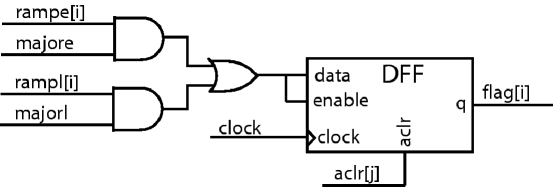
This principle of operation allows defining time-window ranges in units of 6 ns for the CDF XFT. However, hit scanning can be done separately for every bit of the 10-bit data word (this would require configuring the firmware for 10 time -window control bits per channel). In this case the time-window unit would be 1.2 ns 11windows . The 6 ns resolution is thought to be sufficient for the existing XFT system. A block diagram of a time-window register is shown in Figure 8.
Once a register gets set to a high state, it stays high until cleared. The Trigger Logic Control Block sends signals once per event to clear the registers for those time windows whose Trigger Primitives have been calculated and transmitted to the XFT.
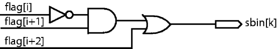
The output Trigger Primitives are computed using the data in the time-window registers with the logic shown in Figure 9. The Trigger Primitive bits consequently depend in a (programmable) Boolean fashion on hits in the 11 time-windows. The first Trigger Primitive bit created per channel every 396 ns corresponds exactly to the result found in the first time-window register. Subsequent bits are Boolean combinations of results found in the later 11 windows.
V.4.2 Trigger Logic Control
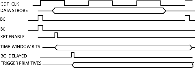
The TDC XFT block analyzes COT data synchronously as they are received. The CDF control pulses Bunch Crossing (BC) and Bunch Zero (B0) are synchronous with the data-stream. Every 12 ns each Hit Finder looks for hits in the input 20 bits in 6 time-windows 11windows . Every 12 ns the Trigger Logic Control block sets 22 bits, two per time-window, to define which 11 time-windows are current for this clock cycle. All Occupancy Detectors get the same 22 time-window bits. These time-window bits are stored in a 22-bit wide RAM, which is accessible via VME. The RAM’s Address Counter is incremented every 12-ns clock and hence the time-window bits refresh every 12 ns. The Address Counter starts to count when it receives an XFT-Enable pulse. The XFT-Enable pulse is delayed by the same amount as the COT data stream relative to the BC and B0 pulses. A sample signal pattern is shown in Figure 10.
The block-diagram of the Trigger Logic Control is shown in Figure 11.
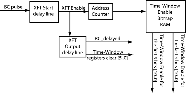
The “XFT-output delay” block sends out a “BC_delayed” pulse which enables the transmission of the Trigger Primitive bits. The “B0_delayed” signal is simultaneous with “BC_delayed”. The delay of the BC pulse depends on the time-windows and can be adjusted to send out trigger bits as soon as each trigger bit is calculated. The delay intervals are controllable by VME-accessible registers. When the transmission of a group of Trigger Primitive bits (48 bits) is finished, the Trigger Logic Control Block clears the corresponding time-window registers by sending out six time-window clear bits (this is asynchronous).
V.4.3 Output Multiplexer
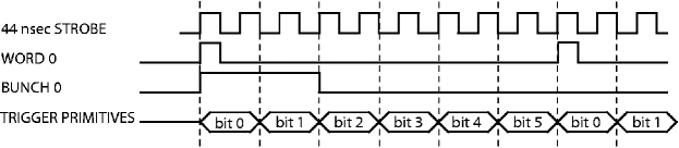
In each TDC Chip the Output Multiplexer (OM) receives the Trigger Primitive bits from the Occupancy Detectors, and Delayed BC and Delayed B0 from the Trigger Logic Control Block. Each OM sends out a 16-bit Trigger Primitive word every 22 ns on the P3 connector to the XFT. The signals are buffered to the P3 connector as TTL levels. The OM also sends synchronously a Word_0 marker (see Table 7), the B0 marker if appropriate (i.e. the crossing is that of the Tevatron bunch 0), and an alignment signal (Data Strobe). The OM does not perform any logical operations on the trigger bits, but sends them in the order required by the XFT Nils_Krumnack .
The existing cables to the XFT have too low a band-width to transmit the 22-ns Main Clock as a data strobe, and so Trigger Primitive bits are sent on the leading and trailing edges of a slower clock which is also transmitted on the cables. The Data Strobe (DS) is a 44 ns clock formed from doubling the period of the Main Clock (see Table 3.) Thirty-two bits, 16 from each TDC Chip, are sent every 22 ns, as shown in Table 7, with 18 such cycles in the beam-crossing period of 396 ns. Figure 12 shows the XFT output timing.
| Clock | Pins 1-17 | Pin 18 | Pin 19 | Pin 23 | Pins 25-33 | Pins 37-43 |
|---|---|---|---|---|---|---|
| Cycle | Wires, Bit | Word0 | B0 | Data_Strobe | Wires, Bit | Wires, Bit |
| 0 | 00-15, bit 0 | High | B0 | High | 48-56, bit 0 | 57-63, bit 0 |
| 1 | 16-31, bit 0 | Low | B0 | Low | 64-72, bit 0 | 73-79, bit 0 |
| 2 | 32-47, bit 0 | Low | B0 | High | 80-88, bit 0 | 89-95, bit 0 |
| 3 | 00-15, bit 1 | Low | B0 | Low | 48-56, bit 1 | 57-63, bit 1 |
| 4 | 16-31, bit 1 | Low | B0 | High | 64-72, bit 1 | 73-79, bit 1 |
| 5 | 32-47, bit 1 | Low | B0 | Low | 80-88, bit 1 | 89-95, bit 1 |
| 6 | 00-15, bit 2 | High | B0 | High | 48-56, bit 2 | 57-63, bit 2 |
| 7 | 16-31, bit 2 | Low | B0 | Low | 64-72, bit 2 | 73-79, bit 2 |
| 8 | 32-47, bit 2 | Low | B0 | High | 80-88, bit 2 | 89-95, bit 2 |
| 9 | 00-15, bit 3 | Low | B0 | Low | 48-56, bit 3 | 57-63, bit 3 |
| 10 | 16-31, bit 3 | Low | B0 | High | 64-72, bit 3 | 73-79, bit 3 |
| 11 | 32-47, bit 3 | Low | B0 | Low | 80-88, bit 3 | 89-95, bit 3 |
| 12 | 00-15, bit 4 | High | B0 | High | 48-56, bit 4 | 57-63, bit 4 |
| 13 | 16-31, bit 4 | Low | B0 | Low | 64-72, bit 4 | 73-79, bit 4 |
| 14 | 32-47, bit 4 | Low | B0 | High | 80-88, bit 4 | 89-95, bit 4 |
| 15 | 00-15, bit 5 | Low | B0 | Low | 48-56, bit 5 | 57-63, bit 5 |
| 16 | 16-31, bit 5 | Low | B0 | High | 64-72, bit 5 | 73-79, bit 5 |
| 17 | 32-47, bit 5 | Low | B0 | Low | 80-88, bit 5 | 89-95, bit 5 |
V.4.4 TDC XFT-DAQ Block
The TDC XFT-DAQ block, used for testing and diagnostic purposes only, connects to a dedicated DAQ system similar to the hit-data stream. It has the same structure, consisting of a ‘Pipeline’, L2 buffers, and VME-readout buffers, and follows the same L1A/L2A sequence as that of the main hit-data stream. The length of the XFT-L2 buffers is also VME controlled. For testing, the XFT block is fitted with another simple VME Readout RAM that contains the current XFT Trigger Primitives. This RAM can be frozen and read out via VME for diagnostic tests, in particular for debugging the TDC-XFT connection.
V.5 The Test Data Generator
The Test Data Pattern Generator inside the TDC Chip allows testing of the functionality of the TDC by running test data through the entire sequence. The Pattern Generator is implemented as a VME accessible dual-port, 512-bit wide RAM, which can store 8192 32-bit words. The first 480 bits of the 512 are used to drive the 48 channels with 10-bit words of test data. In Test- Data Mode, the reading of the RAM is synchronized with the CDF_B0 back- plane signal. The Pattern Generator is used in the tests described below in Section VIII.
V.6 The ASDQ Pulse Generator
The COT electronics chain of ASDQ-Repeater-TDC boards can currently be calibrated by having each TDC send a differential-ECL calibration pulse ‘upstream’ on a pair of dedicated lines in the multi-conductor signal cable to its associated ASDQ cards. Each ASDQ uses this input to generate a calibration pulse at its input, which then propagates back through the data lines of the same signal cable COT . This loop allows a time calibration of the signal path, including the actual cable length. Multiple chains can be calibrated simultaneously by providing the bussed backplane signal CDF_TDC_CALIB to each TDC (see Section IV). The new TDC design provides for the same functionality, but also provides for local generation on the TDC of the pulses to the ASDQ cards. The choice of the two calibration modes is made by VME register selection.
In the local generation mode, the SERDES OUT block (see Figure 4) generates a serial LVDS pulse pattern, available as an ECL signal on the front panel. The timing and number of pulses are controlled via VME by writing the contents of the Tx Pulse Memory, which is implemented as a 10-bit wide, 512-word RAM.
V.7 The Clock Generator Block
The Clock Generator block, implemented in each TDC FPGA with PLL’s, generates the 12-ns and 22-ns clocks used inside the Chip. All the clocks are synchronous with the delayed CDF clock. The prompt CDF clock is also received and is used to latch the CDF-specific back-plane control signals (described in Section IV).
The four 12-ns clocks are generated onto output pins of the FPGA as LVDS signals and routed back into the Chip onto the FPGA’s dedicated high-speed clock input pins, one for each high-speed I/O bank (see Section V.1).
VI The VME interface block
The VME Interface is also implemented with an Altera FPGA Altera_Apex . The design permits Chained Block Transfer (CBLT) read commands in both 32 and 64-bit modes for data transfer. CBLT uses geographical addresses different from the ones normally used in the crate, recognized only by the participating modules. In CDF there are typically 18 TDC cards per VME crate.
There are two possible CBLT read commands:
-
1.
Read Block Transfer from virtual slot 30: Hit Count words are read from every TDC module in the crate. Each TDC produces 14 words/board in 32-bit mode and 8 words/board in 64-bit mode.
-
2.
Read Block Transfer from virtual slot 31: Hit Data words are read from every TDC module in the crate. Each TDC produces up to 336 words/board in 32-bit mode and up to 168 words/board in 64-bit mode.
In this firmware implementation, the CBLT mode is enabled by default. Up to 18 TDC cards sit in a VME crate on the CDF detector; the TDC module closest to the Crate CPU is automatically considered first in the chain. The setting of a module as last in the chain, or the possible removal of a module from the readout, is done by writing to a register in the module’s VME Chip to disable CBLT mode CDF6998 .
VII Power Block
The TDC board receives +5V/15A and -5V/2A on the P0, P1, and P2 backplane connectors. The board generates +1.5V/15A and +3.3V/10A with DC/DC converters, and +2.5V/3A using a linear regulator. A -3.3V voltage is also generated and passed through the front panel connectors to the amplifier-discriminator-shaper card (ASDQ) COT . Spare locations on the TDC board are provided for two additional DC/DC converters.
VIII Testing and Results
The basic idea of the tests is simple: we compare the output of the TDC boards with a reference set, which is computed automatically by the test routines from the input data stored in the RAM in the TDC Chips.
The functionality of the TDC board was checked with a suite of test routines that exercise the Edge Detector (ED48 test), the TDC XFT block (XFT test) and the Chain Block Transfer in both 32-bit and 64-bit modes (CBLT32/64 tests). The following tools are required to test the TDC boards:
All test routines are implemented as C-code, which is executed on the PowerPC (MVME2301 or MVME5500) crate controller after compilation. Other crate controllers can also be used without any significant differences.
The results of these tests are described below in more detail. The burst-mode readout speed achieved in CBLT64 mode is 47 MB/sec. The Edge Detector (ED48) processing time is always less than 12 s (for 7 hits/wire).
VIII.1 The ED48 Test
The ED48 test checks the ED48 logic, internal data paths (RAMS and buffers) and timing of the L1A, L2A, B0, and BC pulses. A block-schema of the test is shown in Figure 13.
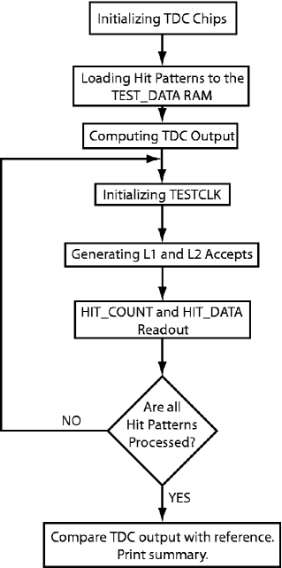
In the beginning of the ED48 test the values in the VME registers are adjusted for the current L1_accept delay (relative to B0), and the TDC is switched to use the Test Data RAM content as an input data-stream. A sample hit pattern is then downloaded to the RAM, which is big enough to hold 15 events. The test program uses the RAM contents to compute the reference output so that it should correspond bit-by-bit to the hardware TDC output. The Testclk Board in the VME crate is initialized to send CDF control pulses to the backplane. One test consists of a set of 15 repetitions (one for every event in the Test Data RAM). At each repetition the L1 Accept and L2 Accept trigger control signals are generated by the Testclk with an incremental delay of 396 ns relative to B0, so that the next event in the Test Data RAM is processed by the ED48. At the end of each repetition (i.e. when the Tdc_Done bit is set- see Section V.3.4), the Hit Data and Hit Count RAMS are read out and the contents stored in a buffer in the Crate Master RAM. After 15 repetitions, when all data from the Test Data RAM have been processed by the ED48 module, the TDC output is compared bit-by-bit with the reference TDC output. The test is passed only if the TDC output is in bit-by-bit agreement with the reference data. During TDC testing the test was repeated thousands times using different hit patterns in the Test Data RAM with no errors.
VIII.2 The TDC XFT Block Test
The TDC XFT block test is very similar to the ED48 Test. The difference is that the output of the TDC XFT block, the XFT Daq RAM, is read out after every L2 Accept instead of the Hit Data and Hit Count RAMs, and the contents compared bit-by-bit with expectations. The test is passed only if the outputs are in a full bit-by-bit agreement. The ED48 and the TDC XFT tests were executed simultaneously using a single routine.
VIII.3 Testing Chain Block Transfer: the CBLT32/64 Test
The CBLT 32/64 tests read out multiple boards in a crate sequentially. Tests were performed with up to 18 TDC boards in a VME crate. The tests are designed to check the VME chain-block transfer capabilities of the board, and also crate-wide characteristics such the crate backplane capability, stability, and multi-board performance.
In the CBLT tests the initial contents of the Level 2 buffer RAMs are used to predict the output of the ED48 modules as read from the Hit Count and the Hit Data RAMs. In the full-crate test 18 TDC boards are used. For each of the 36 TDC Chips in the test (2/board), the L2 buffer lengths are set so that all possible patterns are sampled. The order of accessing the four L2 buffers is also selected differently for each TDC board, so that all combinations of L2 buffer and buffer length are sampled.
Before starting the test cycles the Testclk board is initialized to generate the CDF Clock (132 ns period), required for the PLLs on the TDCs.
Each test cycle first reads the contents of the Hit Count RAMs, and then, using these word counts, the Hit Data RAMs. Both the hit counts and the hit data are compared bit-by-bit with the predicted reference output. The test is then repeated for another combination of L2 buffer sequence assignments and L2 buffer lengths. If an error is detected, a dump of all TDC memories is printed out. The CBLT32 and CBLT64 tests were repeated times each without a single failure.
IX Conclusions and Summary
A new 96-channel TDC has been designed for the CDF Experiment at Fermilab using the multichannel bit-sampling capabilities of the AlteraStratix FPGA family. The board, built in a 9U VME format, contains few other components other than the 2 TDC FPGA’s, a VME controller implemented in a 3rd FPGA, DC-to-DC-converters, and input/output buffers. The functionality is exceptionally flexible, being controlled by firmware, so that it can be reprogrammed for different applications. The TDC has extensive test capabilities, implemented directly in the FPGA’s. Thirty boards have been built and tested. The reliability of the board is high as the chip count is very low. A full crate of the CDF-II TDC has been operated and read out in 64-bit block-transfer mode at a speed of 47 Mbytes/sec.
X Acknowledgments
We thank Bill Badgett, Frank Chlebana, Pat Lukens, Aseet Mukherjee, and Kevin Pitts for help, support, and advice. Nils Krumnack and Ed Rogers deserve special thanks for providing critical input on the XFT specifications and the design of the XFT sections of the TDC. We thank Rich Northrop for the picture of the board.
This work was supported in part by the National Science Foundation under grant number 5-43270, and the U.S. Department of Energy.
References
- (1) CDF Collaboration (T. Affolder et al.); Nucl.Instrum.Meth.A526:249-299,2004.
- (2) The CDF-II detector is described in the CDF Technical Design Report (TDR), FERMILAB-Pub-96/390-E. The TDC described here is intended as a further upgrade beyond that described in the TDR.
- (3) ANSI/VIPA 23-1998, March 22, 1998. These crates support geographical addressing. Chain Block Transfer is described in Appendix E.
- (4) T. Shaw and G. Sullivan, “A Standard Front-End Trigger VME Bus-Based Readout Crate for the CDF Upgrade”, CDF/DOC/TRIGGER/CDFR/2388, May 12, 1998. The CDF readout crate is a 21-slot 9U VME crate based on the VIPA standard, with added bussed signals on rows A and C of the P2 connector. All 64 of the user-defined pins on these rows are bussed between slots 2 and 21 using the same termination scheme as the standard VME bussed lines. Additional power pins are provided on the P0 connector. The J3 backplane, which is physically separate from J1/J2, is customized for I/O specific to each CDF subsystem.
-
(5)
The schematics and test results are available
online at:
http:// edg.uchicago.edu/bogdan/tdc/index.html. The firmware is in CVS at http://www-cdfonline.fnal.gov/cgi-bin/cvsweb.cgi/NuTDC. The schematics and code are available on request. - (6) Any deviation from a linear correspondence with unit slope is due to the quantized nature of the sampling in time bins; the phase-locked loops are much more precise than 1 bin over the full-scale range.
- (7) B. Bevensee et al., IEEE Trans.Nucl.Sci.43:1725-1731,1996, and K. Pitts, private communication.
- (8) Altera Corporation, “Stratix Device Handbook”, v3.0, Apr. 2004. The serializer/deserializer block is labeled SERDES in this Handbook, and in the figures and text here.
- (9) Altera Corporation, “Quartus II Handbook”, v2.1, August 2004.
- (10) Altera Apex AP20K100.
- (11) T. Shaw, Specification for Trigger And Clock + Event Readout Module (TRACER) Terri Shaw; CDF Note: CDF/DOC/ONLINE/PUBLIC/4686; 8/1/98.
- (12) M. Campbell, H. Frisch, M. Shochet, G. Sullivan, D. Toback, J. Wahl, and P. Wilson; Conceptual Design of a Deadtimeless Trigger for the CDF Upgrade; CDF Note: CDF/DOC/TRIGGER/CDFR/2038, April 1993.
- (13) The relative delay between the clock and BC is set in 250 ps steps, determined by values written to a VME register, described in Ref. CDF6998 .
- (14) At initialization the Edge Detector is programmed to assume that four zeros preceded the start of the data stream, so that if the first four bits examined are “True” a hit is registered at the start of the stream.
- (15) The largest leading edge value is actually 254, and not 255, due to the quantization in the pattern recognition algorithm. A leading edge with value 255 would have the pattern ”01111” in the 25th word, starting at bit 5. This register segment is in group B. If this leading edge were written, the possibility also exists that a leading edge starting at bits 4-2 could also be written. These leading edges would have values 256, 257 and 258 respectively. Since those values could not fit into eight-bits, it was decided to make the value of the largest leading edge 254.
- (16) If the ED48 Module is already reading from the Level 2 Buffer, the Level 2 Accept is ignored. The 12 s readout time of the FPGA-based design described here is much shorter than the 500 s of the DSP-based design of the older TDC’s currently used by CDF. The L2 Accept rate is limited to less than 300 Hz, so the deadtime incurred at 12 s is not a problem.
- (17) Run IIb TDC Upgrade: New TDC Implementation in the XFT Ed Rogers, Nils Krumnack CDF Note CDF/DOC/TRIGGER/PUBLIC/7193. This note was crucial to the XFT implementation.
- (18) Mircea Bogdan and Harold Sanders, “Run IIB TDC-II Address Space”, CDF Note 6998, June 2004.
- (19) Note that each time-window bit corresponds to a separate Hit Scanner, which would also have to be implemented in the firmware. This should not be hard, if ever needed. The Occupancy Detector has 11 time-window registers, one for every time-window.
- (20) Both Motorola MVME23001 and MVME5500 processors were used.
- (21) T. Shaw, W. Stuermer, internal note “TESTCLK V7, CDF Crate Clock and Trigger Driver”, Fermilab, ETT/CDF Upgrade Group, July, 1998.
- (22) © 2003 WindRiver Systems, Inc. MCL-DS-VXW-0309.
-
(23)
Jim Pangburn, “FISION V2.12 User’s Guide”,
http://www-cdfonline.fnal.gov/vme/FISION.html. We used VxWorks V5.3c and FISION V2.12 running on a RedHat V6.2 Linux operating system.