Fabrication of micro-mirrors with pyramidal shape using anisotropic
etching of silicon
Abstract
Gold micro-mirrors have been formed in silicon in an inverted pyramidal shape. The pyramidal structures are created in the surface of a silicon wafer by anisotropic etching in potassium hydroxide. High quality micro-mirrors are then formed by sputtering gold onto the smooth silicon (111) faces of the pyramids. These mirrors show great promise as high quality optical devices suitable for integration into MOEMS systems.
The miniaturization of optical components leads to higher packaging density and increased speed of devices that manipulate light. This is part of the vast field of Microsystems technology, designated by Micro-Opto-Electro-Mechanical Systems (MOEMS), in which electronic, mechanical, and optical devices are integrated on the micron scale. Mirrors are fundamental components of most optical systems. A repeatable technique for the fabrication of high-quality micro-mirrrors is therefore an essential step in the advancement of this field. For example, if the surface quality of the mirrors were high enough, one could contemplate using them to make miniature optical resonators, which would have significant applications ranging from narrow-band filters in optical communications Djordjev et al. (2002) to the enhancement or suppression of spontaneous emission in cavity QED devices Kimble (1998). At present there is no simple MOEMS technique to make small mirrors. Small optical cavities have been made using silica and quartz microspheres (see for example ref. [3]), and Coyle et al.Coyle et al. (2003) have reported spherical metallic mirrors fabricated using templated self-assembly, but neither method is ideally suited for integration with MOEMS technology.
We have fabricated 2-dimensional arrays of micro-mirrors in silicon using a method that is simple, economical, and compatible with MOEMS. We start with a -oriented silicon wafer, coated with a thin layer of oxide. Optical lithography is then used to make square openings in the oxide, through which the silicon can be etched. We use the anisotropic etchant potassium hydroxide (KOH) at a concentration of by volume and a temperature of C. This attacks the plane more rapidly than the plane, resulting in a pyramidal pit Brendel (1997) bounded by the four surfaces , , and . Typical resulting pyramids are shown in Fig. 1. The - faces of the pyramids are expected to be extremely smooth because of the layer-by-layer etching mechanism involvedMoktadir and Camon (1997); Sato et al. (1999). Atomic force microscope measurements confirm this, giving an rms surface roughness value of less than nm for the uncoated pyramid faces. This makes them ideal as substrates for high-quality optical mirrors. After stripping the oxide mask away, a layer of gold of 100 nanometers thickness is applied to the silicon. Gold was chosen as it is a good reflector for infrared light, but mirrors for other wavelengths can be made by using other metals or multi-layer dielectric coatings. After sputtering, the surface roughness increases to nm (rms). With this amount of roughness one can calculate that the scattering loss of the specularly reflected intensity should be less than in the near-infrared range Beckmann and Spizzichino (1963). By perfecting the coating procedure it should be possible to decrease these losses to less than in this region of the spectrum.
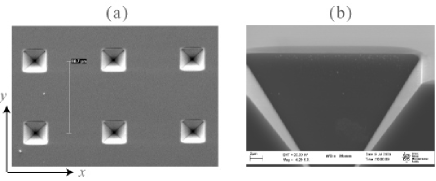 |
Fig. 1 (a) shows a small section of the array viewed under a scanning electron microscope after completion of the gold coating. In this particular sample, the pyramids have a square base whose sides are of m long. These are arranged in a square lattice with a pitch of m. Both the etching and the sputtering processes are standard techniques and can be accurately controlled, guaranteeing that the fabrication results are reproducible. Furthermore, large numbers of mirrors can be packed at high density in a single batch. In the rest of this paper we measure directly how the pyramids respond to light and we show that they offer a promising new approach to fabricating micro-mirrors for MOEMS.
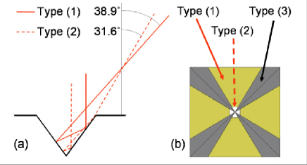
Our first test of the mirrors is to illuminate them with a collimated mm-diameter laser beam (wavelength nm) propagating along the axis, i.e. normal to the silicon surface and along the symmetry axis of the pyramids. The sides of the pyramids define and axes, as shown in Fig. 1. Fig. 2 (a) shows the reflected pattern of light observed on a screen cm away from the mirrors. On this we have drawn circles indicating the position of spots as expected from a perfect pyramid. The three prominent spots at the corners of the square are due to doubly reflected rays, which we classify as type (1). These reflect from opposite faces of the pyramid, as illustrated by the solid line in Fig. 3 (a). There should be a fourth spot at the bottom of the photographs, but this is blocked by a mount holding the beamsplitter through which the array is illuminated.
If the angle between opposite mirrors is , the type (1) beams make an angle of with the axis. From the angles measured, we find that , in agreement with the expected angle between opposing faces of .
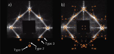
When the incident ray is close to the apex of the pyramid (within m for a pyramid of m base length), it is reflected twice by the first mirror, as illustrated by the dashed line in Fig. 3 (a). These rays, which we call type (2), should produce secondary spots just inside the type (1) spots. However, the power in the type (2) reflected beams is expected to be 100 times smaller because of the small area from which they originate, as shown in Fig. 3 (b). Consequently it is not possible to identify the type (2) beams clearly against the diffracted wings of the type (1) beams. Furthermore, there is a background of light along the - and -axes caused by reflection from rounded edges on the entrance aperture of the pyramid, which can be seen in Fig. 1 (b).
If a ray is incident near one of the corners of the pyramid, the first reflection sends it off towards the opposite mirror, but is is intercepted and deflected by the adjacent mirror before the opposite mirror sends it out of the pyramid as a type (3) ray. These rays make an angle of with the axis and form double spots at azimuthal angles of , etc. as shown in Fig. 2 (a). These spots are less distinct than those of type (1) because the corners of the pyramid are rounded, a feature that does not affect the type (1) rays. Fig. 2 (b) shows the same photographed reflection pattern, but here the superimposed circles indicate the expected position and magnitude of spots reflected from a pyramid with rounded corners. The roundness is included in the ray-tracing model by four additional surfaces at each corner. These are shaped to form approximate cone sections with radii of m at the base and m at the apex of the pyramid. The resulting reflection pattern closely matches the photographed intensity distribution.
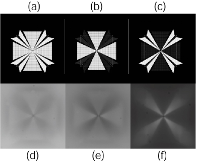
The three types of rays described above also present different characteristics when observed under illumination using polarised light. Type (1) reflections leave the linear polarisation of the light unchanged, whereas the type (3) reflections produce a rotation of or . This is investigated in our second test of the mirrors, in which we examine them under an optical microscope, illuminating them with white light once again along the axis. Fig. 4 (a) shows the image calculated by raytracing for unpolarised light with the microscope focussed in the plane of the apex of a perfect pyramid. In this figure most of the area is bright. In fig. 4 (b) we show the expected image for linearly polarised light, viewed through a parallel analyser, which suppresses the type (3) contribution. This leads to a reduction in the intensity of reflections from the corner region. In Fig. 4 (c), the analyser is crossed with the polariser and only type (3) rays contribute, making the corner region bright. The Intensity patterns observed in the laboratory are shown in figures 4 (d), 4 (e), and 4 (f). They correspond closely to the calculated distributions, indicating that the pyramid reflects light as expected.
Knowing the types of reflected beams and their polarisations one has the possibility of designing the optics to control the field distribution within the pyramid. For example, appropriately angled mirrors can be used to make closed resonant cavities containing only type (1) rays of uniform polarisation. These can be either standing-wave or ring cavities. Rays of type (3) give quite different field distributions with a strong vertical standing wave close to the axis of the pyramid, and horizontal standing waves near the faces of the pyramid. Yet more elaborate field distributions can be achieved by mixing the two. Potential applications for the pyramids are in the areas of atom optics, photonics and telecommunications. For example, by filling the pits with ferroelectric material or liquid crystals and applying an electric field, it should be possible to use the pyramids as fast optical switches.
In summary, we have designed, fabricated and characterized a new type of micro-mirror, produced by anisotropic etching through square apertures on a silicon single crystal. Optical flatness is achieved naturally through the layer-by-layer etching mechanism involved. As an elementary component for optics, the micro-mirror has a variety of possible applications in MOEMS devices, including miniature optical switches and microcavities. Detailed experiments and further theoretical analysis are currently under way to develop these applications.
References
- Djordjev et al. (2002) K. Djordjev, S. J. Choi, and P. D. Dapkus, IEEE Phot. Technol. Lett. 14, 828 (2002).
- Kimble (1998) H. J. Kimble, Physica Scripta T76, 127 (1998).
- LefevreSeguin and Haroche (1997) V. LefevreSeguin and S. Haroche, Mat, Sci. Eng. B 48, 53 (1997).
- Coyle et al. (2003) S. Coyle, G. V. Prakash, J. J. Baumberg, M. Abdelsalem, and P. N. Bartlett, Appl. Phys. Lett. 83, 767 (2003).
- Brendel (1997) R. Brendel, in Proc. 14th European Photovoltaic Solar Energy Conference, edited by H. A. Ossenbrink, P. Helm, and H. Ehmann (Stephens, Bedford, 1997), p. 1354.
- Moktadir and Camon (1997) Z. Moktadir and H. Camon, Modell. Simul. Mater. Sci. Eng. 5, 481 (1997).
- Sato et al. (1999) K. Sato, M. Shikida, T. Yamashiro, M. Tsunekawa, and S. Ito, Sens. and Actuat. A 73, 122 (1999).
- Beckmann and Spizzichino (1963) P. Beckmann and A. Spizzichino, The Scattering of Electromagnetic Waves from Rough Surfaces (Pergamon Press, 1963).