Performance of Hamamatsu 64-anode photomultipliers for use with wavelength–shifting optical fibres
Abstract
Hamamatsu R5900-00-M64 and R7600-00-M64 photomultiplier tubes will be used with wavelength–shifting optical fibres to read out scintillator strips in the MINOS near detector. We report on measurements of the gain, efficiency, linearity, crosstalk, and dark noise of 232 of these PMTs, of which 219 met MINOS requirements.
keywords:
MINOS , Scintillator , Multi-anode photomultiplier tube , wavelength shifting fibre , Hamamatsu , R5900-00-M64 , R7600-00-M64PACS:
42.81.-i Fiber optics , 07.60.Dq Photometers, radiometers, and colorimeters , 29.40.Mc Scintillation Detectors , 14.60.Pq Neutrino mass and mixing1 Introduction
MINOS, a long baseline neutrino-oscillation experiment, uses two large segmented tracking calorimeters to make precise measurements of the atmospheric neutrino oscillation parameters [1, 2]. MINOS uses extruded scintillator strips to form the calorimeter. Wavelength-shifting (WLS) fibres are glued into a longitudinal groove along each strip, so that some of the blue scintillation light is absorbed in the fibre and isotropically re-emitted as green light. A fraction of green light is trapped in the fibre and transmitted along it. At the end of the strip, clear polystyrene fibres carry the light to multi-anode PMTs. Planes of 1 cm thick scintillator strips are sandwiched between 2.54 cm thick planes of steel to form the detectors.
In the MINOS Far Detector, R5900-00-M16 PMTs [3, 4, 5] are used with 8 fibres optically coupled to each pixel in order to reduce the cost of the readout electronics. At the Near Detector, MINOS uses R5900-00-M64 and R7600-00-M64 PMTs111 The R5900-00-M64 and R7600-00-M64 models differ only slightly in that the latter lacks an external mounting flange. Hamamatsu has replaced the R5900 model with the R7600 [6]. (collectively referred to in this work as “M64s”) with one fibre per pixel to avoid reconstruction ambiguities in the higher-rate detector.
Several other experiments have needs similar to MINOS and the same basic technology for reading out scintillator. In particular, OPERA [7] will use M64 PMTs in a tracker similar to MINOS detectors. The proposed MINERA experiment [8] has also chosen M64s as their baseline technology. The K2K SciBar detector uses similar multi-anode PMTs [9]. Scintillating fibre detectors have very similar requirements for PMTs, and M64s have been proposed or adopted by HERA-B [10], CALET [11], GLAST [12], PET detectors [13], and neutron detectors [14]. M64s are also been studied for suitability in RICH detectors by LHCb [15].
In this work we present the analysis of 232 M64 PMTs (13 of which were R7600, the rest of which were R5900) from several production batches, delivered between May 2001 and August 2003. The PMTs included in this sample were those that passed extensive testing and review; out of 232 PMTs tested, 13 PMTs were rejected for use in MINOS by criteria discussed below. The 13 rejected PMTs were not included in the plots and other results presented here.
The basic description of the M64 and the test equipment is described in section 2. For use in MINOS, the PMTs were required to have well-resolved single-photoelectron peak for each pixel, as described in section 3, to ensure high sensitivity. Because of the limited dynamic range of MINOS electronics, a specified uniformity was required between pixels on a single PMT. Uniformity constraints on both gain and efficiency are defined in section 4. Linearity, described in section 5, was measured and was required to reduce the systematic effects when doing calorimetry on high-density showers. The multi-channel nature of the device raised concerns about crosstalk, which is discussed in section 6. Finally, low dark noise, discussed in section 7, is a required feature for MINOS as it reduces load on the data acquisition system.
2 Description of the M64 and test equipment
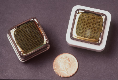
The M64 PMT consists of a single bi-alkali photocathode behind which are focusing electrodes which guide photoelectrons into one of 64 pixels arranged on an 8 by 8 grid. Each pixel is multiplied by a two “metal dynode channels”; each dynode plate has two slits per pixel which act as the multiplying surfaces. Focusing wires are used to keep electrons inside the logical pixel areas. Each pixel is read out by a single anode pad. The active area of each pixel on the PMT window is approximately 1.4 mm1.4 mm. Between pixels is a 0.3 mm space in which efficiency is reduced. The R5900-00-M64 PMT is shown in Figure 1.
The MINOS experiment operates PMTs with the cathodes at negative high voltage and the anodes at ground. A custom-made printed circuit board attached to the base of the PMT provides a voltage-divider circuit to apply voltage to the dynodes in the ratio recommended by Hamamatsu[16] for optimal performance (3:2:2:1:1:1:1:1:1:1:1:2:5). Capacitors are used at the last stages to stabilize the potentials in the case of large instantaneous currents. In addition to the 64 anode signals, a capacitive tap on the 12th dynode was provided on the PCB. The charge on this dynode signal was integrated to provide a simple analog sum of the 64 channels. In the MINOS detector electronics, this dynode signal is used for triggering readout.
| M64 PMTs | |
| Window | 0.8 mm borosilicate |
| Casing | KOVAR metal |
| Size | 28 mm x 28 mm x 20 mm |
| Weight | 28 g |
| Photocathode | bi-alkali |
| Dynode type | metal channel, 12 stages |
| Spectral response | 300 to 650 nm |
| Peak Sensitive Wavelength | 420 nm |
| Anode dark current | 0.2 nA per pixel |
| Maximum HV | 1000 V |
| Gain at 800 V | (typ.) |
| Anode rise time | 1.5 ns |
| Transit spread time | 0.3 ns FWHM |
| Pulse linearity | 0.6 mA per channel |
| Pixel uniformity | 1:3(max) 30%(RMS) |
| WLS Fibre | |
| Manufacturer model | Kuraray double-clad 1.2 mm diameter |
| Material | Polystyrene and polyfluor |
| Fibre Fluor | Y11 |
| Fluor Decay time | 7 ns |
| Clear Fibre | |
| Manufacturer model | As WLS, without fluor |
| Light Source | |
| Source | 5 mm “ultra-bright” blue LED |
| Pulse width | 5 ns |
| Peak wavelength | 470 nm |
Before testing, the M64s were mounted into the MINOS PMT assembly hardware similar to that described in Ref. [4]. First, M64s were glued into uniform Norel collars. These collars were designed to slide tightly into a “PMT holder”. The voltage-divider PCB was attached to the back of the holder, and the front of the holder was attached a “cookie holder”, which provided attachment points for the optical fibre mount. Because the shape of the outer PMT casing does not have a fixed relation to the pixel positions, the cookie holder was aligned with respect to the PMT such that it was centered on alignment marks etched in the first dynode plate. This arrangement allows any fibre cookie to be attached to any PMT with the fibres in the correct positions centered above the pixels. The alignment system had a precision better than 0.1 mm. (Previous measurements [17] have indicated that this precision is adequate to center the fibres. At this precision, the PMT response is reproducible after disassembly and re-alignment.)

For this work, the PMTs were mounted on a test stand illustrated in Figure 2. Each of three PMTs had 64 clear fibres routed to it. The clear fibres were 1.2 mm in diameter, and were fly-cut with a diamond bit to give a polished finish. The PMT was mounted with alignment pins that ensured that the clear fibres were centered on the active pixel areas of the PMT.
Each clear fibre terminated at the center of a hole in an aluminum plate. A stepper-motor system was constructed to move a cylinder (the “light pen”) into any one of these holes. The pen held the end of a green (530 nm) wavelength-shifting fibre. The other end of the 4 m WLS fibre222A four-meter fibre was used to approximate the attenuated light spectrum seen at the end of a MINOS scintillator strip. was illuminated from the side by a blue LED.
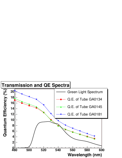
The spectrum of green light from the WLS fibre is shown in Figure 3[18]. The fibre and LED were separated by changeable neutral-density filters which provided different light levels in the tests. The LED was pulsed with a 5 ns wide pulse. The WLS fluor has a decay time of 7 ns, so the light pulse at the PMT was 10 ns FWHM.
In these tests, every channel of the PMT was read out with charge-integrating RABBIT photomultiplier electronics[19]. The LED was pulsed by the RABBIT system. The pulse rate was limited by the data acquisition to about 200 pulses per second. This system used a 16-bit ADC to sequentially read out each channel with a quantization of 0.71 fC per count and a typical resolution of 13 fC RMS per channel. Charges were integrated over a duration of 1.1 s.
Up to three tubes were mounted in the test stand at one time. The fourth position was permanently occupied by an M64 PMT used for monitoring the light level. For each LED flash, one pixel on one PMT was illuminated, and all 64 pixels were read out along with 3 pixels on the monitoring tube. For each complete scan of pixels on the PMT, the three monitor PMT pixels were also flashed to track the light level of the light pulser. Pedestals were subtracted using data taken with the PMT unilluminated.
A complete testing cycle of three PMTs took approximately three days. Four hours were spent allowing tubes to condition to high voltage in the dark. Then scans were taken at varying high voltages for five hours. A nominal operating voltage was chosen automatically, as described in section 4. The tubes were then scanned at each of 11 different light levels (set by the adjustable filter) to test single-photoelectron response, gain, linearity, and crosstalk over the next 13 hours. Then illumination was turned off and dark noise was recorded for the remaining 55 hours, interrupted by two scans to test the stability of the gain measurements.
3 Single Photoelectron Response
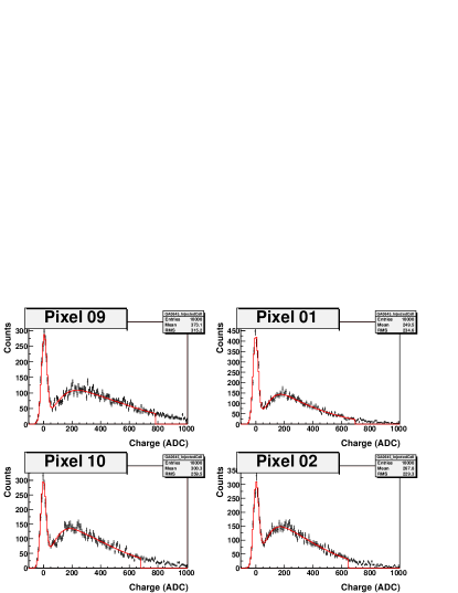
Figure 4 shows the typical charge response for a PMT illuminated at a light level of approximately 1 photoelectron (p.e.) per pulse, with pulses per histogram. The pedestal peak can usually be distinguished from the single–p.e. curve. The voltage is set to the “operating” high voltage described in the following section.
The relative RMS width of the single–p.e. peak is approximately 50% of the mean charge. This large fractional width is due in part to the finite secondary emission ratio of the first dynode, and in part because the two metal dynode channels in each pixel will in general have slightly different gains. In addition to these effects, the electronics resolution broadens the distribution by an additional 8%.
A good fit to the single-p.e. charge spectra was achieved with Eq. (1). First, the mean number of photoelectrons was used to create a Poisson distribution of photoelectrons . Then, for each photoelectrons, the distribution of secondary electrons was again chosen as a Poisson distribution , where represents the mean number of secondary electrons. Each value of is in turn represented by a Gaussian of peak position and width , where is the number of secondary photoelectrons, is the gain, is the electron charge, and is a fit parameter describing the width of the single p.e. peak. The parameter is analogous to the secondary emission ratio of the first dynode, but cannot be interpreted as such due to the broadening effect of two dynode channels[20].
| (1) |
The measured spectra were fit with a Gaussian pedestal peak (with fit parameters of mean, width, and integral) plus the single-p.e. shape given by Eq. 1 (with fit parameters , and ).
Using the fit values of and , the fractional width () of the single-p.e. peak was characterized. The average RMS width of all pixels was 43% 6% of the peak position. (This corresponds to .) The most extreme pixels had widths as high as 58% and as low as 35%.
Five of the 231 PMTs were rejected from the sample for having poor single-p.e. responses: two had totally dead pixels, and three had one or more pixels with very wide or indistinguishable single-p.e. charge spectra.
4 Gains, Efficiencies, and Pixel Uniformity
To test the pixel gains and efficiencies, 10 000 light injections were performed on each pixel at a light level of approximately 10 p.e. per pulse. These data were used to compute the gain and efficiency of each pixel, using photon statistics.
We define as the mean charge of the distribution, as the RMS of the charge distribution, and as the electronics resolution (i.e. the pedestal width), all converted from ADC counts to units of charge (using the gain of the RABBIT electronics). The fractional width of the single-p.e. distribution is given by . If the mean number of p.e. per pulse is , then the gain is defined as
| (2) |
where is the charge of the electron.
The total variance of the charge distribution is the sum of three terms: the variance of the poisson number of photoelectrons created each pulse, the variance due to the finite width of the single-p.e. spectrum, and the variance due to electronic noise:
| (3) | |||||
The gain and number of photoelectrons can then be solved, shown in equations (4) and (5), using only the mean and RMS of the measured charge distribution.
| (4) | |||||
| (5) |
The electronics resolution was typically about 13 fC. For each pixel, the fractional single-p.e. width was taken to be 50%; this simplification created a systematic error on and of only a few percent, similar to the statistical error. Measurements of the gain and efficiency by this method agreed well with the results from the single-p.e. fits described in section 3.
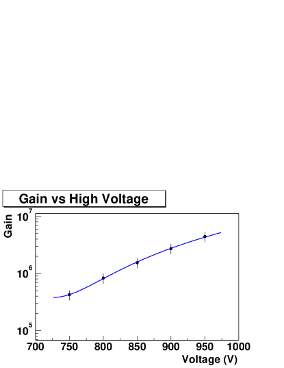
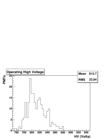
The gain of the PMTs were measured at 750, 800, 850, 900, and 950 V. The mean gain of the 64 pixels at each voltage was calculated and fit to a second-order polynomial for each PMT. One such fit is shown in Figure 5. An operating voltage was found for each PMT such that the mean gain was . The typical slope of the gain curve near the operating HV (expected to be for 12 dynode stages) was 1.5%/V. The distribution of operating voltages for our sample is shown in Figure 6. All subsequent measurements were performed at these operating voltages.
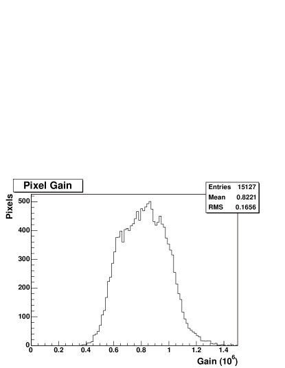
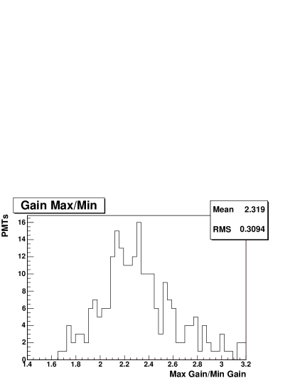
The uniformity of the pixel gains on a single PMT was within 15 to 25% RMS for all accepted PMTs. The histogram of all the pixel gains is shown in Figure 7. Accepted PMTs were required to have a maximum-to-minimum gain ratio of less than about 3 to 1. The histogram of this ratio is shown in Figure 8.
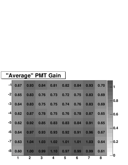
The gain of the pixels followed a repeatable pattern on most PMTs, shown in Figure 9. In particular, pixels 1–8 and 57–64 tended to show the lowest gains on the PMT. (These pixels had larger sensitive photocathode area than the others, so the charge response of the pixels may be more uniform in applications other than fibre readout.) The high–gain pixels near the bottom of the figure are near a small vent used to evaporate the photocathode material during manufacturing; it is possible that this was related to the gain pattern.
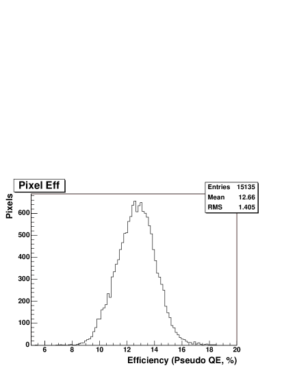
Although no method was available to measure absolute quantum efficiency of the PMTs, the number of measured photoelectrons (for a given light level) could be compared between PMTs. The monitor PMT was used to correct for changes in the LED light level to within one percent. The number of p.e. could then be used to compute the “effective efficiency”, meaning the product of quantum efficiency and collection efficiency integrated over the spectrum of light shown in Figure 3. This effective efficiency was normalized to the 520 nm quantum efficiency of three PMTs evaluated by Hamamatsu to scale to an approximate absolute efficiency.
The efficiency of pixels on a given PMT was more uniform than gain, typically within 10% RMS over 64 pixels. Figure 10 shows the relative efficiencies for all the pixels in the sample. In contrast to the gain measurement, there was no pattern in the efficiencies of pixels at different positions.
Six PMTs were rejected from the sample for having poor inter-pixel uniformity. One or more pixels on each of these PMTs had low gain and sometimes low efficiency as well, creating an unacceptable overall response. These pixels were frequently pixels 1–8 or 57–64, the low-gain columns shown in Figure 9.
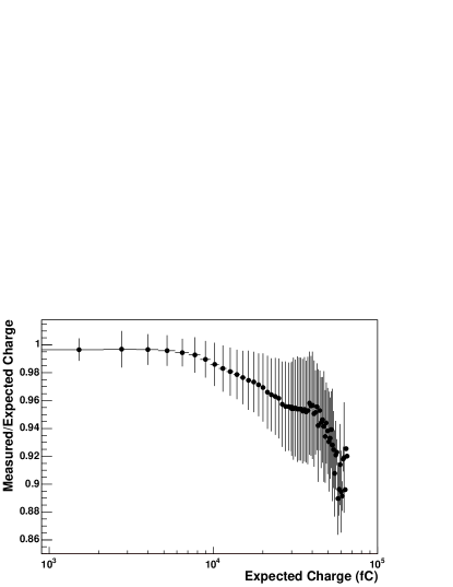
5 Linearity
The small size of the dynodes in an M64 led to a concern that space-charge effects would be large enough to induce nonlinearity at moderate light levels. Figure 11 shows the nonlinearity of pulses in the region from 1000 to 70000 fC. The true intensity of light (in p.e. per pulse) was calculated by assuming the PMTs to be linear when illuminated with a filter to provide 15 p.e, and then calculating the incident light level for a different filter by using the relative filter opacities.333Relative filter opacities were measured in situ by illuminating the LED with DC and measuring the green light with a photodiode. The expected charge for a given pixel was taken as the incident light times the gain times the efficiency of the pixel.
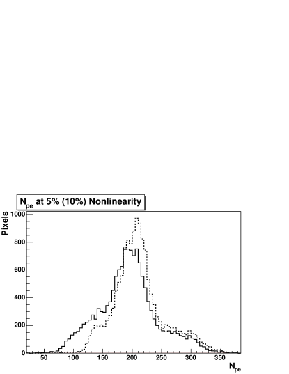
The magnitude of the nonlinearity varied greatly between pixels. The size of the bars in Figure 11 indicate the RMS spread of pixels for the given charge (including a 1% statistical error). This variance can be seen more directly in Figure 12, which indicates the illuminated light level at which pixels become nonlinear. Some pixels remain linear up to 350 p.e., while others become nonlinear at only 70-100 p.e.
For the purposes of MINOS, where signals are expected to be approximately 5 p.e. (for muon tracks) to 100 p.e. (for dense electron showers), these nonlinearities are acceptable. (An in-situ measurement of the nonlinearity will be done in MINOS to ensure accurate calorimetry.[18])
6 Crosstalk
Crosstalk was measured in the test stand by recording the integrated charge on non-illuminated pixels while light was injected onto one pixel. Seven light levels between 10 and 200 p.e. were used.
The crosstalk within the readout electronics was small. The fraction of charge leaked to non-injected pixels was measured to be less than and typically between each pair of pixels. This contribution accounts for only a small proportion of the crosstalk observed.
Crosstalk between pixels on the PMT occurs by two different mechanisms. The first form, “optical” crosstalk, is attributed to primary photoelectrons getting multiplied in the wrong pixel’s dynode chain and thus giving a 1–p.e. signal in the wrong anode. The second form, “electrical” crosstalk, is attributed to electrons leaking from one dynode chain to another near the bottom of the chain, resulting in a small fraction of the injected pixel’s charge moving to the wrong dynode channel or anode.
The non-illuminated pixels showed a small charge on every pulse that was proportional to the charge seen in the injected pixel (i.e. “electrical” crosstalk), and occasionally an additional large charge consistent with a single photoelectron (i.e. “optical” crosstalk). The crosstalk was parameterized for every pair of pixels for every PMT measured in the test stand. Electrical crosstalk was parameterized as the fraction of charge in the injected pixel that was leaked to the non-injected pixel. This was found by observing the shift in the pedestal peak of the non-injected pixel. Optical crosstalk was parameterized as the fractional probability that a given photoelectron would create a signal in the non-injected pixel. Optical crosstalk was found by counting the number of single-p.e. hits in the crosstalk pixel. For both these mechanisms, the mean charge seen in the crosstalk pixel was proportional to the charge seen in the illuminated pixel.
A complete model was built by measuring crosstalk over different light levels and different PMTs. Both electrical crosstalk fraction and optical crosstalk probability were constant with different intensities of injected light. In general, the crosstalk averages were consistent between different PMTs to within about 20%. The values shown below are taken as the average over all light levels.
Crosstalk was strongest between adjacent pixels, but was not limited to this case. Tables 2 and 3 show the fractions of charge that were crosstalked by each of the two mechanisms for the nearest 8 pixels. In summary, approximately 2% of charge in the injected pixel was leaked by electrical crosstalk, and approximately 4% of the photons incident on the injected pixel were detected on the wrong anode. The precision of the values reflects only statistical errors, which were small. Systematic errors on the values in Tables 2 and 3 are about 20%. Poor accuracy was due to the difficulty in separating the two small crosstalk signals. However, the total crosstalk (optical + electrical) could be accurately measured as 6.9% for the whole sample.
In experiments where single-photon response is important the optical crosstalk mechanism dominates. For instance, a signal of a single photoelectron will appear to be on the incorrect pixel 4% of the time, leading to possible problems in interpretation of the data. For large quantities of light the stochastic effects of the optical crosstalk average out so that crosstalk is a simple fraction of the incident light.
| NW | N | NE | ||
| 0.0009 | 0.0036 | 0.0009 | ||
| W | 0.0022 | - | 0.0023 | E |
| 0.0010 | 0.0030 | 0.0010 | ||
| SW | S | SE | ||
| Total to non-neighbors: | 0.0063 | |||
| Total to all pixels: | 0.0212 | |||
| NW | N | NE | ||
| 0.0011 | 0.0054 | 0.0013 | ||
| W | 0.0068 | - | 0.0080 | E |
| 0.0011 | 0.0056 | 0.0012 | ||
| SW | S | SE | ||
| Total to non-neighbors: | 0.0069 | |||
| Total to all pixels: | 0.0374 | |||
7 Dark Noise
M64s were tested for dark noise by taking data with no light on the PMT, with a high voltage of 950 V. The readout system was pulsed times, for an integrated charge-collection time of 44 seconds. Rate was determined by counting the number of readouts for which the integrated charge was greater than a threshold, defined as one-third of a p.e. for the lowest-gain pixel on that PMT. Before conducting the dark noise measurement, the PMTs were under high voltage and exposed to no light for a minimum of 12 hours. The dark noise measurement itself was conducted over two days. The ambient temperature was controlled to be at C.
MINOS specified that PMTs should have total anode noise rates (for all 64 pixels) of less than 2 kHz, but the rates measured for most PMTs were far lower. The average noise rate was 260 Hz per PMT. Approximately 10% of the PMTs had noise rates greater than 500 Hz; approximately 5% had rates greater than 1000 Hz. Two PMTs were rejected from the sample for very high noise rates. The spectra of noise pulses was consistent with a single photoelectron spectrum. It was frequently found that a single pixel would be considerably more noisy than all the others on a PMT; the noisiest pixel contributed on average approximately one third of the total dark noise.
In MINOS, the PMT readout is triggered by a discriminator connected to the tap on the 12th dynode. The signal from this dynode is similar to an analog sum of the individual pixel signals. The rate of pulses on this dynode, using a threshold equivalent to the of a p.e. on the lowest-gain pixel, was found to give consistent results with the method described above.
8 Conclusions
We have found that M64s may be used to provide good measurement of light from wavelength-shifting optical fibres for intensities of 1–100 p.e., the measurement of interest to MINOS. The variance in gain between pixels on a PMT is 25% RMS. Quantum efficiency is similar between PMTs. Excepting a handful of rejected PMTs, the single-p.e. peak was well-resolved from the pedestal at our operating voltage. The PMTs are typically linear for pulses less than 100 p.e. at gain (i.e. 13 000 fC), and are comparable to the 16-pixel R5900-00-M16 PMTs[3]. The M64s have low dark noise, typically 4 Hz per pixel, due to their small pixel area.
Crosstalk in M64s can be a significant problem, particularly if they are used to count single photons since photoelectrons can get collected by the wrong dynode. However, if typical signals are larger, and pixel occupancy small, the adjacent crosstalk signals are easily identified.
In each of the studies described above (single-p.e. response, uniformity, linearity, crosstalk, and dark noise) no significant variation was seen between different delivery batches, or between the R5900 and R7600 models.
We have found M64 PMTs to meet or surpass requirements for reading out scintillator with wavelength-shifting fibres. A total of about 5% of PMTs were rejected for not meeting these requirements. The MINOS near detector, under construction at the time of this writing, will be employing these devices on a large scale.
9 Acknowledgements
We gratefully acknowledge the help and assistance provided by Hamamatsu Photonics Ltd, and thank them for allowing us to reproduce some of their specifications here. We appreciate the assistance of B. Brooks for his help assembling our LED pulser, and P. Sullivan for his work designing and producing the PMT bases. Most importantly, we would like to thank the members of the MINOS collaboration, in particular G. Drake, for his help with instrumentation, K. Ruddick for his work on WLS spectra, J. Alner and T. Durkin for work on PMT boxes and M. Kordosky, and P. Vahle for their work in early pioneering of the techniques with M16 PMTs. This work was funded by the Particle Physics and Astronomy Research Council to which we are grateful for support.
References
- [1] N. Tagg for the MINOS Collaboration , in: Proceedings of the 2nd International Workshop on Neutrino Oscillations in Venice (NO-VE 2003).
- [2] D. Michael, Nucl. Phys. Proc. Suppl. 118 (2003) 189–196.
- [3] K. Lang, et al., Nucl. Instrum. Meth. A461 (2001) 571–573.
- [4] K. Lang, et al., To be submitted to Nucl. Instrum. Meth. (NuMI-NOTE-SCINT-934).
- [5] S. Korpar, et al., Nucl. Instrum. Meth. A442 (2000) 316–321.
- [6] H. Moyses, Hamamatsu Photonics UK Ltd, Private communication.
- [7] P. Migliozzi, Int. J. Mod. Phys. A18 (2003) 3877–3894.
- [8] D. Drakoulakis et. al. (The MINERA Collaboration), arXiv:hep-ex/0405002 (February 2004).
- [9] K. Nitta, The K2K SciBar detector, arXiv:hep-ex/0406023 (2004).
- [10] E. C. Aschenauer, et al., Nucl. Instrum. Meth. A424 (1999) 459.
- [11] T. Tamura, in: Proceedings of the ICRC 2001, Copernicus Gesellschaft, 2001, p. 2297.
- [12] K. Rielage, et al., Nucl. Instrum. Meth. A463 (2001) 149.
- [13] Y. Shao, S. Cherry, A. Chatziioannou, Nucl. Instrum. Meth. A477 (2002) 486.
- [14] A. Gorin, et al., Nucl. Instrum. Meth. A479 (2002) 456.
- [15] E. Albrecht, et al., Nucl. Instrum. Meth. A488 (2002) 110–130.
- [16] Hamamatsu Photonics K.K., 314-5 Shimokanzo, Toyooka-village, Iwata-gun, Shizuoka-ken, 438-0193, Japan, Multianode photomultiplier tube R5900-00-M64 Data Sheet (Jan 1999).
- [17] M. A. Barker, et al., arXiv:hep-ex/0203001 (2002).
- [18] P. Adamson, et al., Nucl. Instrum. Meth. A492 (2002) 325–343.
- [19] G. Drake, T. Droege, S. Kuhlmann, J. C.A. Nelson, Nucl.Instrum.Meth. A269 (68).
- [20] A. Cabrera, et al., NuMI tech. note NuMI-NOTE-SCINT-934, University of Oxford, available at http://www-numi.fnal.gov/cgi-bin/notePublicPrint (2003).
- [21] Photomultiplier Tubes: Principle to Comment Application, Hamamatsu Photonics K.K., 1994.