The role of wire imperfections in micro magnetic traps for atoms
Abstract
We present a quantitative study of roughness in the magnitude of the magnetic field produced by a current carrying microwire, i.e. in the trapping potential for paramagnetic atoms. We show that this potential roughness arises from deviations in the wire current flow due to geometric fluctuations of the edges of the wire : a measurement of the potential using cold trapped atoms agrees with the potential computed from the measurement of the wire edge roughness by a scanning electron microscope.
pacs:
39.25.+k, 03.75.BeThe use of micro or even nano-fabricated electrical devices to trap and manipulate cold atoms has attracted substantial interest, especially since the demonstration of Bose-Einstein condensate using such structures ReichelNature ; ZimmermannPRL . Compact and robust systems for producing BEC’s, single mode waveguides and possibly atom interferometers can now be envisaged. The small size of the trapping elements, usually current-carrying wires producing magnetic traps, and the proximity of the atoms to these elements (typically tens of microns), means that many complex and rapidly varying potentials can be designed Folmanrevue . This approach has some disadvantages however. On the one hand it has been shown that atoms are sensitive to the magnetic fields generated by thermally fluctuating currents in a metal when they are very close Folmanrevue ; Zimmermann-fragPRA2002 ; Hinds-heating2003 ; Vuletic-VdW ; Cornell-spinfliplosses . On the other hand, a time independent fragmentation of a cold atomic cloud has been observed when atoms are brought close to a current carrying micro-wire Zimmermann-fragPRA2002 ; Ketterle-guide2002 ; Hinds-frag2003 .
This fragmentation has been shown to be due to a potential roughness arising from distortions of the current flow in the wire Zimmermann-frag2002 ; Ketterle-opttrap . It has also been demonstrated experimentally that the effect of these distortions decreases with increasing distance from the wire Hinds-frag2003 ; Zimmermann-frag2002 . In an attempt to account for the observations, a theoretical suggestion has been made that the current distortions may be simply due to geometrical deformations, more specifically meanders, of the wire Lukin-frag2003 . In this paper we show that for at least one realization of a microfabricated magnetic trap, using electroplating of gold, this suggestion is substantially correct. We have measured the longitudinal density variation of a fragmented thermal cloud of atoms trapped above a wire, and inferred the rough magnetic potential. We have also made scanning electron microscope images of the same wire and measured the profile of the wire edges over the region explored by the atoms. The magnetic potential as a function of position deduced from the edge measurements is in good quantitative agreement with that inferred from the atomic density. We suspect that this result is not unique to our sample or fabrication process and we emphasize the quantitative criterion for the necessary wire quality to be used for atom manipulation.
The wires we use are produced using standard microelectronic techniques. A silicon wafer is first covered by a 200 nm silicon dioxide layer. Next, layers of titanium (20 nm) and gold (200 nm) are evaporated. The wire pattern is imprinted on a 6 m thick photoresist using optical lithography. Gold is electroplated between the resist walls using the first gold layer as an electrode. After removing the photoresist and the first gold and titanium layers, we obtain electroplated wires of thickness m with a rectangular transverse profile (see Fig. 1). A planarizing dielectric layer (BCB, a benzocyclobutene-based polymer) is deposited to cover the central region of the chip. On top of the BCB, a 200 nm gold layer is evaporated to be used as an optical mirror for light at 780 nm. The distance between the center of the wire and the mirror layer has been measured to be 14(1) m.
The magnetic trap is produced by a current flowing through a Z-shaped microwire Reic99 together with an external uniform magnetic field (along the -axis, see Fig. 1) parallel to the chip surface and perpendicular to the central part of the wire. The central part of the Z-wire is 50 m wide and 2800 m long. Cold 87Rb atoms, collected in a surface magneto-optical trap, are loaded into the magnetic trap after a stage of optical molasses and optical pumping to the hyperfine state. The trap is then compressed so that efficient forced evaporative cooling can be applied. Finally, the trap is decompressed. Final values of and vary from 200 mA to 300 mA and from 3 G to 14 G respectively so that the height of the magnetic trap above the wire ranges from 33 m to 170m. An external longitudinal magnetic field of a few Gauss aligned along is added to limit the strength of the transverse confinement and to avoid spin flip losses induced by technical noise. For these parameters, the trap is highly elongated along the -axis. The transverse oscillation frequency is typically kHz and 120 Hz for traps at 33 m and 170 m from the wire respectively.
The potential roughness is deduced from measurements of the longitudinal density distribution of cold trapped atoms. The atomic density is probed using absorption imaging after the atoms have been released from the final trap by switching off the current in the Z-wire (switching time smaller than 100 s). The probe beam is reflected by the chip at 45o allowing us to have two images of the cloud on the same picture. From images taken just after (500 s) switching off the Z-wire current we infer the longitudinal density . We also deduce the height of the atoms above the mirror layer from the distance between the two images. The temperature of the atoms is determined by measuring the expansion of the cloud in the transverse direction after longer times of flight (1 to 5 ms).
To infer the longitudinal potential experienced by the atoms, we assume the potential is given by
| (1) |
where is a transverse harmonic potential. Under this separability assumption, the longitudinal potential is directly obtained from the measured longitudinal density of a cloud at thermal equilibrium using the Boltzmann law . To maximize the sensitivity to the longitudinal potential variations, we choose a temperature of the same order as the variations ( K for traps at 170 m from the wire and K for traps at 33 m from the wire). The separability assumption has been checked experimentally by deducing a -dependent oscillation frequency from the rms width of the transverse atomic density at different positions. At 33 m from the wire, there is no evidence of a varying oscillation frequency. At a height of 170 m above the chip, over a longitudinal extent of 450 m, we deduce a variation of the transverse oscillation frequency of about 13%. In this case, the assumption of separability introduces an error of in the deduced potential.

The potential experienced by the atoms is . To a very good approximation, the magnetic field at the minimum of is along the -axis (for our parameters, the deviation from the -axis is computed to be always smaller than 1 mrad) so that the longitudinal potential is given by . For a perfect Z-wire, the longitudinal potential is solely due to the arms of the wire and has a smooth shape. However, we observe a rough potential which is a signature for the presence of an additional spatially fluctuating longitudinal magnetic field. A spatially fluctuating transverse magnetic field of similar amplitude would give rise to transverse displacement of the potential which is undetectable with our imaging resolution and small enough to leave our analysis unchanged.
In the following, we present the data analysis which enables us to extract the longitudinal potential roughness. In order to have a large statistical sample and to gain access to low spatial frequencies, one must measure the potential roughness over a large fraction of the central wire. In our experiment, however, the longitudinal confinement produced by the arms of the Z-wire itself is too strong to enable the atomic cloud to spread over the full extent of the central wire. To circumvent this difficulty, we add an adjustable longitudinal gradient of which shifts the atomic cloud along the central wire. We then measure the potential above different zones of the central wire. We typically use four different spatial zones which overlap each other by about m. We then reconstruct the potential over the total explored region by subtracting gradients from the potentials obtained in the different zones. Those gradients are chosen in order to minimize the difference between the potentials in the regions where they overlap.
We are interested in those potential variations which differ from the smooth confining potential due to the arms of the wire. We thus subtract the expected confining potential of an ideal wire from the reconstructed potential. To find the expected potential, we model the arms of the Z by two infinitesimally thin, semi-infinite wires of width 250 m, separated by a distance and assume a uniform current distribution. We fit each reconstructed potential to the sum of the result of the model and a gradient, using the gradient, and the distance above the wire as fitting parameters. The fitted values of differ by a few percent from the nominal value 2.8 mm, while we find m where is the distance from the mirror as measured in the trap images. This result is consistent with the measured 14m thickness of the BCB layer.
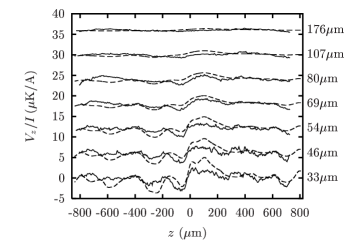
The potential which remains after the above subtraction procedure is plotted for different heights in Fig. 2. For a fixed trap height (fixed ratio ), we have checked that the potential is proportional to the current in the wire; therefore we normalize all measurements to the wire current. The most obvious observation is that the amplitude of the roughness decreases as one gets further away from the wire. The spectral density of the potential roughness is shown in Fig. 3 for two different heights above the wire. We observe that the spectrum gets narrower as the distance from the wire increases (see inset in Fig. 3). This is expected since fluctuations of wavelength much smaller than the height above the wire are averaged to zero. At high wave vectors (m-1 at 33 m and m-1 at 80 m) the spectrum exhibits plateaus which we interpret as instrumental noise. We expect this noise level to depend on our experimental parameters such as temperature, current and atomic density. Qualitatively, smaller atom-wire distances, which are analyzed with higher temperatures should result in higher plateaus. This is consistent with the observation.
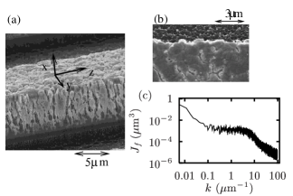
In the following we evaluate the rough potential due to edge fluctuations of the central wire. For this purpose, the edges of the wire are imaged using a scanning electron microscope (SEM), after removal of the BCB layer by reactive ion etching. Figure 4(a) indicates that the function , which gives the deviation of the position of the wire edge from the mean position , is roughly independent of . We make the approximation that depends only on . We deduce from SEM images taken from above the wire (see Fig. 4(b)). To resolve , whose rms amplitude is only m, we use fields of view as small as 50 m. The function is reconstructed over the entire length of the central wire using many images having about 18 m overlaps. As shown in Fig. 4(c), several length scales appear in the spectrum. There are small fluctuations of correlation length of about 100 nm and, more importantly, fluctuations of larger wavelength (60 to 1000 m).

The geometric fluctuations of the edges of the wire induce a distortion of the current flow which produces a longitudinal magnetic field roughness responsible for a potential roughness. To compute the current density in the wire, we assume a uniform resistivity inside the wire. We also assume that fluctuations are small enough to make the current density distortion linear in , where are the fluctuations of the left and right edge of the wire respectively. The current density is in the -plane and, because the rough potential is proportional to the longitudinal magnetic field, we are only interested in its component, . Because of symmetry, only the part of which is even in contributes to in the -plane. Thus, only the symmetric component is considered. The Fourier component of induces a transverse current density Lukin-frag2003
| (2) |
As the distances from the wire we consider (33 to 176 m) are much larger than the thickness of the wire m we will in the following assume an infinitely flat wire. To efficiently compute the longitudinal magnetic field produced by these current distortions, we use the expansion on the modified Bessel functions of second kind , which is valid for . This expansion is, in the -plane,
| (3) |
where
| (4) |
being the modified Bessel function of the first kind. For small wave numbers such that , one expects the coefficients to decrease rapidly with . Indeed, for , . In our data analysis, only wave vectors smaller than m-1 are considered for which so we expect the coefficients to decrease rapidly with . In the calculations, only the terms up to are used.
Equations 2,4 and 3 then allow us to compute the fluctuating potential from the measured function . In Fig. 3, we plot the spectral density of the potential roughness calculated from for two different heights above the wire (33 and 80 m) and compare it with those obtained from the potential measured with the atoms. For both heights, and for wave vectors small enough so that the measurements made with the atoms are not limited by experimental noise, the two curves are in good agreement. As we have measured the function on the whole region explored by the atoms, we can compute directly the expected potential roughness. In Fig. 2, this calculated potential roughness is compared with the roughness measured with the atoms for different heights above the wire. Remarkably the potential computed from the wire edges and the one deduced from the atomic distributions have not only consistent spectra but present well correlated profiles. We thus conclude that the potential roughness is due to the geometric fluctuations of the edges of the wire. The good agreement between the curves also validates the assumption of uniform conductivity inside the wire used to compute the current distortion flow.
In conclusion, we have shown that the potential roughness we observe can be attributed to the geometric fluctuations of the wire edges. Fluctuations at low wave vectors, responsible for most of the potential roughness, correspond to wire edge fluctuations of very small amplitude compared to their correlation length. We emphasize that a quantitative evaluation of these wire roughness components demands dedicated measurement methods.
Furthermore, wire edge fluctuations put a lower limit on the possibility of down-scaling atom chips. For a given fabrication technology the wire edge fluctuations are expected to be independent of the wire width . Thus assuming a white noise spectrum, the normalized potential roughness varies as for fixed ratio , being the distance to the wire Lukin-frag2003 . In order to reduce the potential roughness, one must pay careful attention to edge fluctuations when choosing a fabrication process. For example, we are currently investigating electron beam lithography followed by gold evaporation. Preliminary measurements indicate a reduction of the spectral density of the wire edge fluctuations by at least two orders of magnitude for wave vectors ranging from 0.1 m-1 to 10 m-1. This should allow us to reduce the spectral density of the potential roughness by the same factor unless a new as yet unobserved phenomenon such as bulk inhomogeneity sets a new limit on atom chip down-scaling Schmiedmayer .
We thank C. Henkel and H. Nguyen for helpful discussions. This work was supported by E.U. (IST-2001-38863, HPRN-CT-2000-00125), by DGA (03.34.033) and by the French ministry of research (Action concert e "nanosciences-nanotechnologies").
References
- (1) W. H nsel, P. Hommelhoff, T. W. H nsch, and J. Reichel, Nature 413, 498 (2001).
- (2) H. Ott, J. Fortágh, G. Schlotterbeck, A. Grossmann, and C. Zimmermann, Phys. Rev. Lett. 87, 230401 (2001).
- (3) R. Folman et al., Adv. Atom. Mol. Opt. Phys. 48, 263 (2002), and references therein.
- (4) J. Fortágh, H. Ott, S. Kraft, A. Gunther, and C. Zimmermann, Phys. Rev. A 66, 41604 (2002).
- (5) M. P. A. Jones et al., Phys. Rev. Lett. 91, 080401 (2003).
- (6) Y. J. Lin, I. Teper, C. Chin, and V. Vuletic, Phys. Rev. Lett. 92, 050404 (2004).
- (7) D. Harber, J. McGuirk, J. Obrecht, and E. Cornell, J. Low Temp. Phys. 133, 229 (2003).
- (8) A. E. Leanhardt et al., Phys. Rev. Lett. 89, 40401 (2002).
- (9) A. E. Leanhardt et al., Phys. Rev. Lett. 90, 100404 (2003).
- (10) M. P. A. Jones et al., J. Phys. B: At. Mol. Opt. Phys. 37, L15 (2004).
- (11) S. Kraft et al., J. Phys. B 35, L469 (2002).
- (12) D. Wang, M. Lukin, and E. Demler, Phys. Rev. Lett. 92, 076802 (2004).
- (13) J. Reichel, W. Hänsel, and T. W. Hänsch, Phys. Rev. Lett. 83, 3398 (1999).
- (14) P. D. Welch, IEEE Trans. Audio and Electroacoustics AU-15, 70 (1967).
- (15) Measurements by the Heidelberg group of an atom chip produced by photolithography and gold evaporation indicates reduced potential roughness compared to other observations. J. Schmiedmayer, private communication. S. Groth et al., cond-mat/0404141 (2004).