The CMS Si-Strip Tracker
Abstract
The CMS experiment at LHC features the largest Silicon Strip Tracker (SST) ever build. This device will be immersed in a 4T magnetic field in conjunction with a Pixel system allowing the momentum reconstruction of charged particles and the heavy-flavor tagging despite the hostile radiation environment. The impact of the operating conditions and the physics requirements on the SST layout and design choices is discussed and the expected performances are reviewed.
1 Requirements and Implications
The Compact Muon Solenoid (CMS) experiment will observe pp collision at of center-of-mass energy with a luminosity of . The bunch crossing frequency is and minimum bias interactions per bunch crossing are expected, resulting in charged tracks per event and a hadron flux up to close to the interaction region.
The physics requirements, a momentum resolution of at and an impact parameter resolution of , have to be obtained by instrumenting a cylindrical volume of 5.4m in length and 2.4m in diameter immersed in a 4T axial magnetic field. The innermost region () is occupied by a pixel detector, described elsewhere[1]. The CMS collaboration decided to instrument the remaining volume by using only Silicon microstrip modules organized in 10 cylindrical layers and 12 disks as sketched in Figure 1, corresponding to more than of active surface. A detailed description of the Silicon Strip Tracker (SST) and its expected performances can be found elsewhere[2]. Only a brief overview is given here.
2 The Tracker Layout
The tracker is divided into four main subsystem: the innermost four cylindrical layers make up the Inner Barrel (TIB); the outermost six cylindrical layers define the Outer Barrel (TOB); the disks with between and are the Inner Disks (TID), each organized in three rings; the bigger disks in the region, organized in four to seven rings, are the Endcaps (TEC).
Most SST modules are single sided; the “barrel” modules and the “disk” modules have the readout strips laying along the direction and the radial direction, respectively, allowing the readout of the coordinate; however some threedimensional information is needed to separate tracks. A space point readout is obtained by using a double-sided module, a back-to-back sandwich of a module and a special stereo module with the strips tilted by . Double-sided modules equip the two innermost layers of TIB and TOB, the two innermost rings of TID, and the TEC rings with and with (see Figure 1). This layout allows the SST to provide 8 to 14 measurements points for high momentum tracks with . On average about half of them are threedimensional points.
3 The modules
The overall dimensions of the SST, the largest device of this kind ever built, require such a huge number of basic elements to impose an industrial approach to the design and the production. The SST modules and their components share the same basic structure and design. Each module consists of a carbon fiber frame that supports the silicon detector and the readout electronics, hosted on a front-end hybrid.
The modules have to comply with the following characteristics: a pitch of the order of to ensure the target momentum resolution; radiation resistance with no significant performance degradation for the 10-years of LHC lifetime; high granularity in time (low pile-up, i.e. shaping time) and in the space domain (occupancy below , i.e. a cell size of , corresponding to a strip length of the order of ) to ensure a robust and efficient pattern recognition.
All the SST detectors are standard p+-on-n microstrip sensors with AC readout and polysilicon bias resistor, produced by single-sided lithographic process on 6”-wafer industrial lines, thus allowing an effective cost reduction. The sensor radiation hardness relies upon several features[3]: special design details like multi-guard rings, the constant width-over-pitch of 0.25, and the metal over-hang (metal strips wider than underlying implants) effectively improve the breakdown voltage behavior; the use of low-resistivity bulk () allows the sensors to be depleted at a manageable voltage over the entire LHC lifetime also after the type inversion; an interstrip capacitance almost fluence independent is obtained by using the lattice orientation that gives a Si-SiO2 interface of better quality.
Nevertheless, the SST operating and storage temperature must be below to keep under control the radiation-induced increase of the leakage current and to freeze-out the unwanted reverse annealing.
A key design aspect of the SST to limit the costs and the number of readout channels relies upon the scaling of track multiplicity and radiation effects with the radius. Occupancy requirement imposes sensors within in radius to have a pitch of and a strip length of . To limit the number of readout channels this requirement is relaxed at choosing a pitch of and a strip length of , obtained by daisy-chaining two single sensors. Similarly, thick sensors with resistivity are needed for to have a comfortable depletion voltage after the irradiation but, for , less expensive thick sensors with resistivity can be safely chosen, also to compensate the increase of noise due to the larger strip length. The various shapes and dimensions of the SST detectors are shown in Figure 2(a) and the evolution of strip length and pitch is shown in Figure 2(b).


The front-end hybrid is made of a kapton circuit (that also integrates the connection tail) laminated onto a ceramic rigidifier. It hosts four or six APV25s, the SST front-end chips, the additional ASICs (APVMUX, PLL and DCU) and the pitch adapter that allows the APV25 channels’ pitch to match the sensors’ one.
The APV25 has been designed in CMOS technology for low-noise and fast signal readout in high radiation environment. It has 128 charge-sensitive amplifying channels with shaping time multiplexed into a single readout line. A deconvolution filter is implemented to reduce the time resolution to . A pipeline buffer stores analog samples for 192 bunch crossings, corresponding to , to match the LVL1 trigger requirements. Further details on the front-end hybrids and a description of the downstream readout chain can be found elsewhere[4].
The assembly of the modules needed to complete the entire SST is performed by means of semi-automatic gantries featuring pattern recognition for an accurate and reproducible placement of the components with tolerances that are comparable with the intrinsic resolution of the device (). Similarly the M bonds required to connect sensors are made by automatic bonding machines.
Production is actually starting. A tight quality assurance procedure is strictly enforced at each production/assembly step to check that all components match the required specifications. These tests normally include cooling cycle to reproduce the actual working condition.
4 Mechanics and Material Budget
The modules support structure is made up of carbon fiber and honeycomb frames. It ensures a mechanical stability within and the absolute position accuracy needed by track finding and alignment procedures[5]. The structure also hosts services like readout lines, power cables and cooling pipes (to take out ) and has been designed to grant easy access and operation on all subelements.
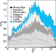
Despite all optimization efforts to keep the SST as light as possible the contribution of active material, structures, electronics and services results into a substantial material budget. Figure 3(a) shows the result of the detailed GEANT4 simulation in terms of radiation lengths as a function of pseudorapidity .
5 Performance
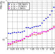
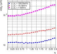
The resolution, shown for muons in Figure 3(b), is or better for and ; at larger pseudorapidity the performance degrades because of the reduction of the lever arm. The transverse impact parameter (IP) resolution, shown in Figure 3(c), is in the entire range covered by the tracker, for muons of . Low momentum and IP resolutions are degraded by the multiple scattering. The track reconstruction efficiency is close to 100% for muons in most of the pseudorapidity range, while it drops to for pions and tracks within jets, mostly because of nuclear interactions.
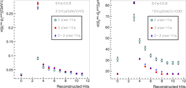
As shown in Figure 4(a) and (b), sufficient track reconstruction accuracy is achieved by using the pixel hits and a reduced number of silicon strip hits, tipically four to six. Such figures demonstrate the redundancy and the robustness of the SST layout and the possibility to use fast tracking algorithms for trigger applications[6].
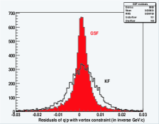
The negative impact of the large material budget on the SST performances can be reduced by designing reconstruction algorithms that take into account the presence of material. As an example, electrons suffer for large material-dependent bremsstrahlung energy losses. A precise modeling of this effect has been implemented in a special electron reconstruction algorithm[7] by using the Gaussian-sum Filter (GSF), a non-linear generalization of the standard Kalman Filter (KF). The impressive gain in resolution of this special electron reconstruction algorithm is shown in Figure 4(c).
6 Conclusion
The present silicon strip technology allows the CMS collaboration to build a large scale tracker despite the difficult operating environment of a high-luminosity, high-energy hadron collider. Detailed simulation studies suggest that the SST performances will lay within the physics requirements. The layout redundancy makes possible to use fast-tracking algorithms at trigger level. The effects of the relatively large amount of material inside the tracking volume can be taken into account by accurate modeling and dedicated algorithms.
References
- [1] D. Kotliński, “The CMS Pixel Detector”, these proceendings.
- [2] CMS Collaboration, “The Tracker System Project Technical Design Report”, CERN-LHCC/98-6 (1998); CMS Collaboration, “Addendum to the CMS Tracker TDR”, CERN-LHCC/2000-16 (2000).
- [3] S. Braibant et al., Nucl. Ins. Meth. A485, 343 (2002).
- [4] K. Klein, “The CMS Silicon Strip Tracker: System Test and Test Beam Results”, these proceendings.
- [5] S. Koenig, “The CMS Tracker Alignment System”, these proceendings.
- [6] CMS Collaboration, “The TriDAS Project Technical Design Report, Volume II: Data Acquisition & High-Level Trigger”, CERN-LHCC/2002-26 (2002).
- [7] W. Adam, R. Fruhwirth, A. Strandlie and T. Todorov, eConf C0303241 (2003) TULT009 [arXiv:physics/0306087].