New Results on DEPFET Pixel Detectors for Radiation Imaging and High Energy Particle Detection
Abstract
DEPFET pixel detectors are unique devices in terms of energy and spatial resolution because very low noise (ENC = 2.2e at room temperature) operation can be obtained by implementing the amplifying transistor in the pixel cell itself. Full DEPFET pixel matrices have been built and operated for autoradiographical imaging with imaging resolutions of 4.30.8 m at 22 keV. For applications in low energy X-ray astronomy the high energy resolution of DEPFET detectors is attractive. For particle physics, DEPFET pixels are interesting as low material detectors with high spatial resolution. For a Linear Collider detector the readout must be very fast. New readout chips have been designed and produced for the development of a DEPFET module for a pixel detector at the proposed TESLA collider (520x4000 pixels) with 50 MHz line rate and 25 kHz frame rate. The circuitry contains current memory cells and current hit scanners for fast pedestal subtraction and sparsified readout. The imaging performance of DEPFET devices as well as present achievements towards a DEPFET vertex detector for a Linear Collider are presented.
I Introduction
For a Linear Collider Detector [1] efficient and good flavor identification and separation is required for the accurate determination of Higgs branching ratios and other physics processes beyond the Standard Model. However, due to the very prominent beamstrahlung near the interaction point, the background conditions and the time structure of the accelerator are fierce leading to detector occupancies of 80 hits / mm2 / bunch train ( 1ms) for a typical pixel detector situated at a radius of 15 mm away from the beam line. DEPFET pixel detectors have shown to be capable of simultaneously providing excellent energy and spatial resolution which can be exploited for various applications: imaging in biomedical autoradiography [2, 3, 4], imaging of low energy X-rays from astronomical sources [5, 6, 7, 8] and particle detection at a future Linear Collider [9, 10, 11]. In this paper we present the achievements obtained to date in imaging and spectroscopy with DEPFET pixel devices and describe the developments for a micro vertex detector based on DEPFET pixels for a Linear Collider. The DEPFET developments for the XEUS project are presented by L. Strüder [8] at this conference.
II The DEPFET principle and operation
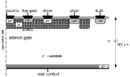
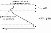
The DEPleted Field Effect Transistor structure [12], abbreviated DEPFET, provides detection and amplification properties jointly. The principle of operation is shown in fig. 1. A MOS or junction field effect transistor is integrated onto a detector substrate. By means of sidewards depletion [14], appropriate bulk, source and drain potentials, and an additional deep-n-implantion a potential minimum for electrons is created right underneath the transistor channel ( 1 m below the surface). This can be regarded as an internal gate of the transistor. A particle entering the detector creates electron-hole pairs in the fully depleted silicon substrate. While the holes drift into the rear contact of the detector, the electrons are collected in the internal gate where they are stored. The signal charge leads to a change in the potential of the internal gate, resulting in a modulation of the channel current of the transistor.
The simultaneous detection and amplification feature makes DEPFET pixel detectors very attractive for low noise imaging [3, 15]. For particle detection the use of very thin (m) detectors operated with very low power consumption should be possible. The low noise operation is obtained because the capacitance of the internal gate can be made very small (several 10 fF), much smaller than the cell area suggests. Furthermore, no external connection circuitry to the first amplification stage is needed. External amplification enters only at the second level stage. This leads to an excellent noise performance already at room temperature. The pixel delivers a current signal which is roughly proportional to the number of collected electrons in the internal gate. Signal electrons as well as electrons accumulated from bulk leakage current must be removed from the internal gate after readout. Clearing is obtained by periodically applying a positive voltage pulse to a clear contact. Other clear mechanisms have also been studied [4]. The question, whether the internal gate is completely emptied from electrons upon a CLEAR pulse (complete CLEAR) is an important one, both for very low noise operation in X-ray astronomy with XEUS and for fast pedestal subtraction in a LC detector. With complete clearing the statistical fluctuations in the number of electrons in the internal gate as well as switching noise (kT/C noise) are absent.
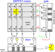
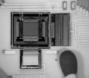
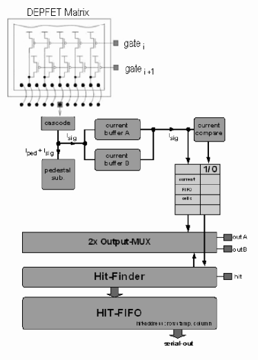
A DEPFET matrix is operated as shown in fig. 2. Rows are selected by applying a voltage to the external gate of a row. Drains are connected column-wise. The drain current of each pixel in a selected row is detected and amplified in a dedicated amplification circuit. Pedestals are taken at the beginning of an exposure cycle and subtracted off-line. Finally, clear pulses are applied to the clear contacts to empty the internal gates. On the right of fig. 2 a photograph of a DEPFET-Matrix hybrid assembly as used for imaging is shown. Both, gate-on/off and CLEAR pulses are issued from the sequencer chip on the right.
III Performance of DEPFET single pixels and matrices
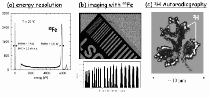
Figure 3 summarizes the performance figures obtained with DEPFET single pixels and with a 64x64 DEPFET matrix, respectively. Fig. 3(a) shows the measured energy spectrum obtained with a single DEPFET pixel structure at room temperature. Using circular structures of a recent production energy resolutions of 131 eV at 6 keV (55Fe, Kα peak) have been measured, originating from a Fano noise contribution of 14e and a DEPFET noise contribution of 2.2e. Figure 3(b) displays the image of precision slits in a tungsten test chart, the smallest of which are 25m wide at 50m pitch. The projection of the image is shown below in fig. 3(b). An evaluation of the measured structure results in a width of the point spread function of = 6.7 0.7 m using an 55Fe (6 keV) X-ray source and = 4.3 0.8 m using a 109Cd (22 keV) source, corresponding to MTF30% values of 37 lp/mm and 57 lp/mm, respectively [4]. The corresponding width of the point spread function for Tritium imaging derived from these measurements is 7m. Fig. 3(c) finally shows the autoradiogram of a tritium-labelled leaf imaged with a 64x64 DEPFET pixel matrix. The ability to simultaneously distinguish different radio labels (3H and 14C) in real time has also been demonstrated [4].
Beyond the development for autoradiography, we are presently developing DEPFET pixels for imaging with the X-ray telescope of the planned XEUS satellite of the European Space Agency ESA [8, 16], and for a particle micro vertex tracker for a future Linear Collider like TESLA [1, 9]. While for XEUS very good energy resolution (ENC 4e) at relaxed frame times (1.2 ms) is required, at TESLA frame times of 50s for 520x4000 pixels and 50m thin detectors are needed.
IV Developments for a Vertex detector for TESLA
For a pixel detector at TESLA, DEPFET pixels can offer
-
•
50m thin detectors with S/N values still in excess of 50.
-
•
A total material budget (sensor, chips and frame) of 0.11X0: The 50m thin sensors sit in a perforated 300m silicon frame (see section IV-B).
-
•
A cell size of 25x25m2 or similar.
-
•
A fast readout with 50 MHz line rate and 25 kHz frame rate for 520x4000 pixels per module
-
•
Low power consumption of 5W for the entire detector with 5 barrel layers as proposed for TESLA [1].
IV-A New DEPFET Sensors
Based upon the encouraging performance of DEPFET single structures and large matrices, new DEPFET structures tailored to the needs of the XEUS (75m diameter circular structures) and TESLA (small 2025m2 linear structures) projects have been fabricated at the MPI Semiconductor Laboratory in Munich using a design with 2-metal layers. Among the main design goals were
-
•
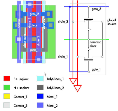
smaller pixels by a factor of 2 in both linear dimensions: This enforced the change from closed circular JFET geometries, used so far, to linear MOSFET structures, for which smaller devices with better homogeneity and reproducibility over a large area can be made with the existing technology. In order to reduce the size further cells containing two pixels with a common clear structure, a common source and two drain contacts have been produced (see fig. 4). One row addresses always a pair of pixels with the drains connected to two separate column like output busses.
-
•
One of the main drawbacks of the previous structures was the uncomplete clearing of the internal gate, limiting the ability to obtain the achieved single pixel noise figures below 5e also in large matrices. While complete clearing of the internal gate is mandatory for low energy X-ray imaging with XEUS, it is also necessary for operation with TESLA speeds, because here signal and pedestal currents are on-chip subtracted with a CLEAR pulse being applied between subsequent signal and pedestal samplings (c.f. section IV-C. In order to facilitate this operation a ClearGate structure has been added around the entire pixel cell, which is activated shortly ( 10 ns) after the CLEAR pulse. A ClearGate structure with the required dimensions is very difficult to fabricate with a JFET realization of the DEPFET transistor.
Simulations have confirmed that no potential pockets, which can trap signal charges during charge collection and clearing, are present in the design.
The smallest structures of the present production are about 20x30 m2. First measurements on single structures using an 55Fe X-ray source have confirmed the excellent noise performance of previous structures. With the low noise circular structures designed for the XEUS project, an ENC of 2.2 e- and 131 eV FWHM for the Kα line have been measured at room temperature. The charge to current amplification has been measured to be 400pA/e on the first structures which have been evaluated. Figure 5 indicates that complete clearing has been achieved. Shown is the width of the noise peak obtained by measuring the DC DEPFET drain current using two very different R/O operations: (a) one CLEAR and then taking 500 R/O samples, (b) taking 500 x (CLEAR + R/O) samples. If the clearing is complete the widths of the noise peaks in both cases should be the same. This is the case for sufficiently large CLEAR pulses with sufficient duration time (e.g. 14V, 100 ns pulse width).

Very first studies on DEPFET matrices indicate DEPFET current dispersions of about 7.5 over a 16128 pixel matrix operated without clearing. The space resolution has not yet been measured in test beams yet. Extrapolating from measurements with previous DEPFET pixel matrices with cell dimensions of 50m50m we expect space resolutions for minimum ionizing particles with these new sensors in the order of 2-4m, depending on the charge sharing between pixels.
IV-B Wafer thinning technology
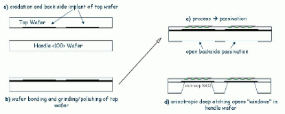
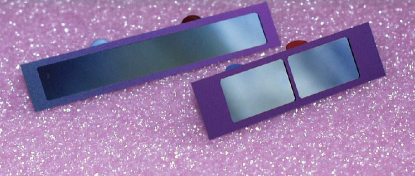
Thinning of DEPFET wafers using anisotropic etching has been developed successfully in collaboration with the MPI für Mikrostrukturphysik in Halle/Germany [17]. The processing steps using bonding of a handle wafer are shown in fig. 6. A thin 50m structure which is stiffened by a frame of thicker silicon ( 350m) is obtained. The detector remains sensitive also in these thicker frame regions. Active Si diodes have been thinned this way with very satisfactory results and leakage currents less than 1 nA/cm2 [17] have been measured. A photograph of thinned passive, module sized samples is presented in fig. 7.
IV-C Readout chips for DEPFET modules at a LC
The readout principle for a DEPFET matrix of fig. 2 is unchanged for a much faster operation at a Linear Collider. However, a module of 520x4000 pixels is read out column-wise to both top and bottom sides at a continuous line rate of up to 50 MHz (40s frame time) in the innermost layer, taking 25 frames per train crossing time ( 1 ms). Both, the row addressing sequencer chip SWITCHER for (external) gate on/off and (internal gate) clear and the column-based current readout chip (CURO) for amplification and sparsified current readout must comply to this rate. During one line cycle (20 ns), sampling of signal+pedestal, CLEAR, and sampling of pedestal is required.
The block diagram of the readout chip CURO is shown in fig. 8. A cascode stage at the input of the readout chip keeps the drain lines at a constant potential, such that the DEPFET current does not need to charge the relatively large bus capacitance. A row is selected for readout after the charge accumulation interval. The selected DEPFET transistors output a signal current superimposed to a pedestal current. This current is stored in a current memory cell for every column. After a complete CLEAR of the row, and assuming negligible leakage currents during the time between two sample cycles (10 ns), the pedestal current is measured by a second sampling cycle in the selected row. The pedestal subtracted signal is then obtained by summing the stored (negative) signal+pedestal current with the pedestal current. The signal current is stored in an analog FIFO of several current memory cells. A fast current comparison with a programmable hit threshold generates a digital hit pattern which is simultaneously recorded in a digital FIFO. Analog FIFO cells with no hits can be switched off to save power. While the analog FIFOs are filled with events containing at least one hit, a fast scanner searches for hits in the digital FIFO. The corresponding analog values are selected with a multiplexer and fed to one or several ADCs.
Crucial elements of this design are the current memory cell, the hit scanner, and the current comparator. They have all been tested using a test chip fabrication. The current memory cell (fig. 9) is adopted using the switched current technique [18]. A current is stored in three phases:
-
1.
Storage Phase: S1 and S2 are closed, S3 open. The gate capacitance of the transistor M1 is charged until the device provides the combined input and bias current ().
-
2.
Sampling Phase: S2 is opened. The gate voltage and therefore the transistor current ideally remain unchanged.
-
3.
Transfer Phase: Immediately after sampling S1 is opened and S3 closed. As the current through M1 is still , must be delivered by the output node.
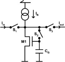
Thus, in the ideal case . However, this simple circuit suffers from several non-ideal effects like charge-injection of the sampling switch S2 and the limited output conductance of the transistor M1 and the biasing current source. Therefore in the real case where indicates the error made by the sampling process. Many techniques to cope with these deficiencies have been treated in the literature [19]. Here, cascode techniques have been used for the sampling transistor and the current source to decrease the output conductance. The implemented circuitry uses a two stage design to cancel charge injection and to achieve a high dynamic range with a small storage error. Measurements using a test chip at a 25MHz sampling rate (limited by the test setup) show a differential non-linearity of over a sufficiently large dynamic range of 10 A corresponding to several mips. At the cost of linearity the total dynamic range can be as large as 100A, corresponding to the charge of 20 mips or more, depending on the gq of the DEPFET transistor. The total standing current in the memory cell operated at a supply voltage of V is so that for the input stage the calculated power consumption is per DEPFET column. The hit finder uses a binary tree structure as first proposed in [20] to find two hits out of a pattern of 128 digital inputs within one clock cycle. Measurements on the hit finder circuitry implemented on the test chip confirm that a speed of 50MHz is easily achievable in the chosen technology. A full chip for a 64x128 DEPFET matrix has been submitted using radiation tolerant design rules. One important of the many advantages of the switched current based technique is its little dependence on smaller and smaller becoming operating voltages in advanced IC technologies.
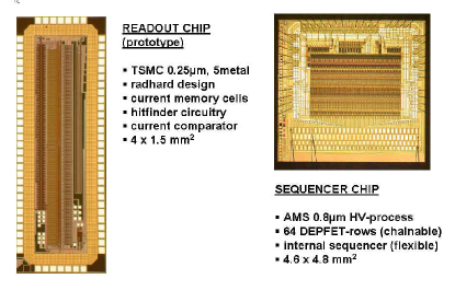
The sequencer chip (SWITCHER) generates high voltage (20V) signals for gate on/off and CLEAR of rows. In order to provide a wide voltage range for testing of the first matrices, a special ’high voltage’ 0.8 technology has been chosen. The chip (photo in fig. IV-Cb) contains 64 channels with analog multiplexers, a digital sequencer and control logic. It is designed to be suited for of all fabricated DEPFET matrices for the different applications including 50MHz operation at TESLA. Several chips can be daisy chained to control larger arrays. Measurements on the fabricated prototype chip show that it is fully functional at 30 MHz speed. By addressing 2 pixels at the same time (see fig. 4) the target line rate for TESLA would be 25 MHz, i.e. a time of 40 ns per line, during which sampling of the signal current, CLEAR, and sampling of the pedestal current must be done.
The total power consumption has been calculated using measured currents and voltages of prototype detectors and chips, and assuming that rows can be switched off while not being read out. Scaled to the total pixel vertex detector [1] of TESLA with 5 layers, the sensor is expected to have a power consumption of 0.3W, while the ICs consume 3-4W (SWITCHER) and 1-2W (CURO), respectively. Hence, we consider a total power budget of less than 5W for the entire detector to be feasible. This figure renders air cooling or alternative low mass cooling to be possible, hence offering a very low total material budget ( 1 X0).
V Conclusion
In contrast to other trends in monolithic or semi-monolithic pixel detector developments (see e.g. [21, 22]), partially using incomplete charge collection, DEPFET pixels excel in excellent energy (ENC = 2.2e, =131 eV) and space (4.3 m at 20 keV X-rays) resolutions. This can be exploited in a variety of applications. In biomedical autoradiography the excellent imaging performance of DEPFET pixels has been demonstrated by space resolved imaging of Tritium-labelled biological tissue. A spatial resolution for 3H of 7m as inferred from measurements with X-ray sources has been concluded. For the future use of DEPFET pixels for X-ray astronomy within the ESA-XEUS mission or for high energy particle vertex tracking, smaller and, in terms of resolution, still better performing DEPFET structures have been developed. For use at a future Linear Collider a R/O architecture integrated circuits have been developed with speeds larger by a factor 1000 than achieved so far. These include a current based R/O chip with fast and low noise current memory cells and a current-hit finder.
Acknowledgment
The authors would like to thank the technology crew of PN sensor GmbH and MPI at the Semiconductor Laboratory.
References
- [1] T. Behnke, S. Bertolucci, R. D. Heuer and R. Settles, TESLA: The superconducting electron positron linear collider with an integrated X-ray laser laboratory, Technical Design Report, Part 4, DESY-01-011 (2001).
- [2] W. Neeser, P. Fischer, M. Löcker, J. Ulrici, N. Wermes, H. Matthaey, P. Buchholz, P. Klein, H. Koch, M. Trimpl, N. Hörnel, J. Kemmer, G. Lutz, L. Strüder, The DEPFET Pixel BIOSCOPE, IEEE Trans. Nucl. Sci. 47 No.3 (2000).
- [3] J. Ulrici, S. Adler, P. Buchholz, P. Fischer, P. Klein, M. Löcker, G. Lutz, W. Neeser, R. Richter, L. Strüder, M. Trimpl, N. Wermes, Spectroscopic and imaging performance of DEPFET pixel sensors, Nucl. Inst. & Meth. A 465 247 (2000).
- [4] J. Ulrici, P. Fischer, P. Klein, G. Lutz, W. Neeser, R. Richter, L. Strüder, M. Trimpl, N. Wermes, Imaging Performance of a DEPFET Pixel Bioscope in Tritium Autoradiography, submitted to IEEE Trans. NS (2003).
- [5] P. Holl, P. Fischer, P. Klein, G. Lutz, W. Neeser, L. Strüder, N. Wermes: Active Pixel Matrix for X-ray Satellite Missions IEEE, Trans. Nucl. Sci, Vol. 47, No. 4 (2000).
- [6] P. Klein, P. Buchholz, P. Fischer, N. Hörnel, P. Holl, J. Kemmer, M. Löcker, G. Lutz, W. Neeser, D. Stötter, L. Strüder, M. Trimpl, J. Ulrici, J. Vocht, N. Wermes, First Measurements on a DEPFET Active Pixel Matrix for X-Ray Imaging Spectroscopy SPIE conference on UV, Optical and IR Space telescopes and Instruments, Proceedings SPIE Conference, Munich 2000, Vol. 4013, pp. 605 - 611.
- [7] L. Strüder et al, Fully Depleted, backside illuminated, spectroscopic active pixel sensors from the infrared to X-rays, Proceedings SPIE Conference, Munich 2000, Vol. 4012 (2000).
- [8] L. Strüder, Position Resolved Room temperature Spectroscopy with the Silicon X-ray Active Pixel Sensor DEPFET. Paper submitted to IEEE03-RTD Conference on Room Temperature Devices, Portland Oct. 2003.
- [9] R. Kohrs, M. Karagounis, H. Krüger, I. Peric, M. Schumacher, M. Trimpl, J. Ulrici, N. Wermes, P. Fischer, M. Harter, L. Andricek, G. Lutz, R. Richter, M. Schnecke-Radau, G. Schaller, F. Schopper, L. Strüder, J. Treis, K. Heinzinger, P. Lechner, H. Soltau, A DEPFET Pixel Vertex Detector for TESLA, DESY Report PRC RD 03/01, April 8th, 2003.
- [10] R.H. Richter, L. Andricek, P. Fischer, K. Heinzinger, P. Lechner, G. Lutz, I. Peric, M. Reiche, G. Schaller, M. Schnecke, F. Schopper, H. Soltau, L. Str der, J. Treis, M. Trimpl, J. Ulrici, N. Wermes, Design and Technology of DEPFET Pixel sensors for linear collider applications, Vertex 2002 Conference, Nov. 2002, Hawaii, Nucl. Instr. & Meth. A 511, 250 (2003).
- [11] M. Trimpl, L. Andricek, P. Fischer, G. Lutz, R.H. Richter, L. Strüder, J. Ulrici, N. Wermes, A Fast Readout using Switched Current Techniques for a DEPFET-Pixel Vertex Detector at TESLA, Nucl. Instr. & Meth. A 511, 257 (2003).
- [12] J. Kemmer, G. Lutz, New semiconductor detector concepts, Nucl. Instr. & Meth. A 253, 356 (1987).
- [13] J. Kemmer, G. Lutz et al, Experimental confirmation of a new semiconductor detector principle, Nucl. Instr. & Meth. A 288, 92 (1990).
- [14] E. Gatti, P. Rehak, Semiconductor drift chamber - An application of a novel charge transport scheme, Nucl. Instr. & Meth. A 225 608 (1984).
- [15] G. Cesura et al., New pixel detector concepts based on junction field effect transitors on high resistivity silicon, Nucl. Instr. & Meth. A 377, 521 (1996).
- [16] XEUS astrophysics working group, X-ray evolving universe spectroscopy- the XEUS science case, ES, SP-1238 (2000).
- [17] L. Andricek et al., Processing of Ultra Thin Silicon Sensors for Future Linear Collider Experiments, paper submitted to this conference.
- [18] J. B. Hughes, N. C. Bird, I. C. Macbeth, Switched Currents - A New Technique for Analog Sampled Data Signal Processing, Proc. of Int. Symp. Circuits and Systems (ISCAS), Portland, Oregon, May 1989, pp. 1584–1587
- [19] B.E. Jonsson, Switched-Current Signal Processing and A/D Conversion Circuits, ISBN 0-7923-7871-7
- [20] P. Fischer, G. Comes, H. Krüger, Mephisto - a 128 channel strip readout chips with real-time data sparsification and multi-hit-capability, Nucl. Instr. & Meth. A 431 134–140 (1999).
- [21] N. Wermes, Trends in Pixel Detectors: Tracking and Imaging, Review Paper submitted to this conference.
- [22] G. Deptuch et al., Monolithic Active Pixel Sensor with In-pixel Double Sampling and Columns-level Disrcrimination, Poster submitted to this conference.