\conferencereport2003/052
{Authlist}
K. KLEIN
\InstfootcernI. Physikalisches Institut B, RWTH Aachen
52074 Aachen, Germany
E-mail: Katja.Klein@physik.rwth-aachen.de
\collaborationOn behalf of the CMS Tracker Collaboration
With a total area of 210 squaremeters and about 15000 single silicon modules the silicon strip tracker of the CMS experiment at the LHC will be the largest silicon strip detector ever built. While the performance of the individual mechanical and electronic components has already been tested extensively, their interplay in larger integrated substructures also has to be studied before mass production can be launched, in order to ensure the envisaged performance of the overall system. This is the main purpose of the system tests, during which hardware components as final as possible are being integrated into substructures of the tracker subsystems. System tests are currently being carried out for all subsystems of the tracker. In addition, silicon modules and electronic components have been operated and studied in a particle beam environment. In this report results from the CMS silicon tracker system tests and a test beam experiment at CERN are presented.
\conferencePresented at the 8th ICATPP Conference, Como, Italy, October 6-10, 2003
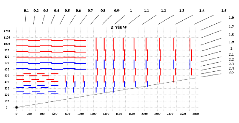
1 The CMS Silicon Strip Tracker
The CMS silicon strip tracker is divided into four subsystems: the Tracker
Inner Barrel and Inner Disks (TIB and TID), the Tracker Outer
Barrel (TOB) and the Tracker End Caps (TEC). The modularity of the system can
be seen in Fig. 1, where one quarter of the detector is shown
in the longitudinal view. The total tracker will be cooled
to an operating temperature of – C. A detailed description of the
layout of the silicon strip tracker is available in Ref. [1] and
references therein.
Silicon modules mounted within a radial distance of 60 cm from the beam
line have 320 m thick sensors, while the sensors of all outer modules
have a thickness of 500 m. Single- and
double-sided modules are used, the latter being made of two single-sided
modules mounted back-to-back with a stereo angle of 100 mrad. The sensor
design is described in Ref. [2].
The TIB consists of four cylindrical layers. Each layer is constructed out
of two carbon fiber (CF) half-shells per beam (z) direction. Strings carrying
three thin modules are mounted inside and outside of the layer surfaces.
The TOB is composed of six cylindrical layers. The basic structure of the
TOB is a rod: a CF support frame, which carries either three
double-sided (layers 1-2) or three single-sided (layers 3-6) thick
modules on each side.
Finally, each of the two endcaps of the TEC consists of nine CF
disks. On each disk 16 petals, wedge shaped CF support plates which carry up
to 28 modules arranged in seven radial rings, are mounted.
The readout is based on the APV25 chip[3] built in radiation hard
0.25 m CMOS technology. This 128 channels chip implements a
charge-sensitive amplifier, a shaper and a 192 cells pipeline (3.2 s
long). Two
operation modes can be chosen: in peak mode only one data sample is
processed, while in deconvolution mode three consecutive samples
are summed with weights. This leads to a much shorter pulse and thus to
correct bunch crossing identification in the high luminosity phase of the LHC.
The signals of two chips are multiplexed onto one data line and converted
to optical ones in Analog Opto-Hybrids (AOHs)[4]. The data are then
transmitted to the control room, where VMEbus readout boards called Front End
Drivers[5] (FEDs) provide opto-electrical conversion,
digitization and zero-suppression.
The monitoring and control is handled by Front End Controller (FEC)
VMEbus cards, which communicate via a digital optical
link[4] in a token ring protocol
with dedicated Communication and Control Units (CCU25)[6] mounted
on the string/rod/petal motherboards. These chips distribute the control
signals
to the addressed modules, while trigger and clock signals are propagated to
Phase Locked Loop (PLL) chips on the front-end hybrids.
2 Results from System Tests and the May 2003 Beam Test
System tests are currently
being carried out for all subsystems of the tracker: for the TOB at
CERN, for the TIB/TID in Florence and Pisa and for the TEC in Aachen and Lyon.
Both electrical behaviour, with emphasis on the noise and signal-to-noise
performance, and the cooling performance are being
studied and the design is qualified or optimized, if necessary.
For the TIB and TEC the most complete system tests up to now
have been realized in a test beam environment at CERN during May 2003.
The X5 beam
in the CERN West Area provided muons and/or pions (= 120 GeV/ for
pions). The beam had a LHC-like time structure, with about 3 nsec long
particle bunches, spaced by 25 nsec time periods.
The main difference between test beam and system test setups
and the final CMS readout and control chains is that currently PCI mezzanine
cards (PMC) are used for readout and control (PMCFED[7] and PMCFEC)
instead of the final VMEbus cards. These PMC have no implementation of
optical conversion, thus additional opto-electrical converters are
necessary.
In the following the setups of the TEC and TIB beam tests and the TOB
laboratory system test, along with first preliminary results, are described.
2.1 Test Beam Data Acquisition
In the test beam the most recent DAQ software, based on the
XDAQ[8] framework, was used. For the first time, a prototype of
the final run control[9] was available, and an online
monitoring programme provided immediate feedback on the performance. For
each subsystem (TIB, TOB, TEC) optical transmission
of data as well as timing and control signals between the control room and
the beam area was realized. Each subsystem used one PC with a PMCFEC and a
second PC housing two or three PMCFEDs and a Trigger Sequencer Card,
which distributed the particle trigger and the clock from the
TTC system[10] to the FEC and the FEDs.
The commissioning of the individual subsystems was finished within about two
hours. This included the tuning of
the optimal FED sampling point, the adjustment of the timing difference
between individual channels due to their different positions in the trigger
distribution path, the optimization of AOH parameters (adjustment of the
laser diode gain and bias current, to be repeated for each temperature
change) and finally trigger latency and PLL delay scans to find the physics
signal (the sampling point which gives the highest signal to noise).
Automatized procedures are implemented in the software for all these tasks.
Mostly the TIB, TEC and TOB subsystems were read out
independently of each other, but finally the TIB and
TOB DAQ systems were merged and the two subdetectors read out coherently
like a single detector after only a few hours of commissioning. This shows the
scalability and commissioning capability of the DAQ software.
2.2 The Tracker End Cap Beam Test
For the first time a prototype of a
TEC petal, equipped with nine modules (four thin single-sided modules on
ring four, four thick single-sided modules on ring six, plus one thick
double-sided module on ring five), was studied in a test beam. Twelve
front-end hybrids plus AOHs were
distributed on the remaining positions. The petal was cooled via its own
cooling pipe system and was kept inside a thermally and electrically
isolated passive cooling box, flushed with dry
nitrogen. Temperature and humidity inside the box were monitored and an
interlock on the low voltage was implemented. Floating power supplies
(not of the final design) were used for low voltage and also for high voltage
to bias the detectors.
Both low and high voltages were transmitted to the petal via
45 m long cables of the final design.
The system showed excellent performance in terms of the signal-to-noise ratio
(S/N). The S/N distributions of all modules have been studied in peak mode
running for a bias voltage of 350 V and an operating temperature of
C. In Fig. 2 (a) two examples are shown:
S/N Landau peaks of 27 and 39 are found for a thin and
a thick module, respectively.
In Fig. 2 (b) the S/N of the same thick (ring five)
module is compared for running at C and at room
temperature, under otherwise identical conditions. The
S/N is increased significantly when the module is operated at C,
compared to operation at room temperature, where a S/N of only 33.5 is
measured.


Figure 3 shows the results of bias voltage scans.
For a ring four module a plateau in S/N is reached for a
voltage of 190 V. A double-sided ring five module consists of two
single-sided modules, each with two daisy-chained wafers, mounted with a
stereo angle. For the two sensors of one single-sided
ring five module the plateau voltages are 264 V and 265 V. It was
possible to distinguish between the two sensors since the stereo angle
was exploited to calculate the radial coordinate along the
strip direction. In this way the clusters can be assigned to the individual
sensors. The plateau voltage is higher than the depletion voltage, since
charge collection is incomplete without significant overdepletion.
High plateau voltages at the start ensure that after type inversion due to
irradiation only moderate bias voltages must be applied to maintain full
efficiency.

2.3 The Tracker Inner Barrel Beam Test
The TIB test beam setup consisted of a part of a half-shell of
layer three with four strings. Two of these strings were equipped with three
single-sided thin modules each, while the CCU25 and the mothercable were
mounted for all four strings. The
TIB setup was thermally stabilized at room temperature. Temperature and
humidity were monitored and interfaced to an interlock system. Two different
protoypes of the final control room power supplies (from
CAEN and LABEN), supplying both low and high voltage,
as well as a 125 m long low inductance power cable of the final design were
studied for their noise behaviour, and exhibited excellent performance.
The noise of the system was found to be very low. The common mode subtracted
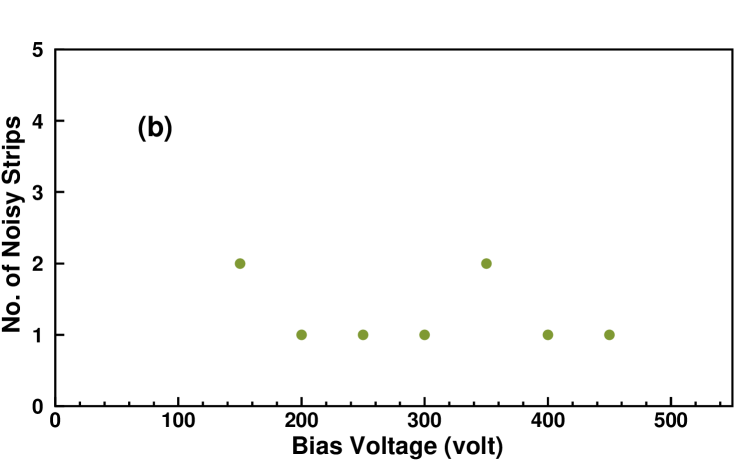
noise of a typical TIB module is shown in Fig. 4 (a).
The mean common mode subtracted noise is only 0.97 ADC counts. In Fig. 4 (b) the
dependence of the number of noisy strips of one module on the bias
voltage is shown. The number of noisy strips is very small and stable.
The signal pulse shape, measured with a muon beam, has been reconstructed in
peak and deconvolution mode. While in peak mode a (slightly adjustable)
peaking time of about 55 nsec is found, in deconvolution mode the pulse
is much sharper and the peaking time is below 20 nsec. This is known to be
achieved at the cost of a lower S/N. However, with a typical
Landau peak of 18 (for 300 V bias voltage), the S/N in deconvolution mode is
still sufficiently high. In peak mode a S/N of about 26 is measured.

2.4 The Tracker Outer Barrel System Test
The system test of the TOB is in a very advanced state. The system test
of a single-sided rod is finished and the design has been validated.
Currently a double-sided rod equipped with twelve – modules is under
test at CERN, and a CMS Note summarizing the results is in preparation.
The noise performance of the rod was tested extensively. A comparison
between a single module setup, consisting of a bare module, and
the rod setup equipped with the same module shows compatible noise and
common mode both in peak and deconvolution mode.
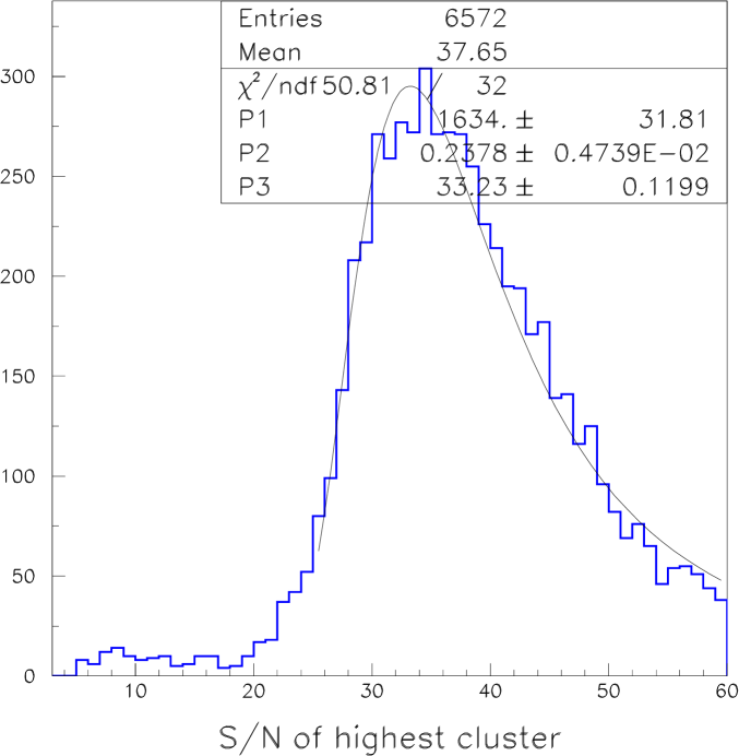
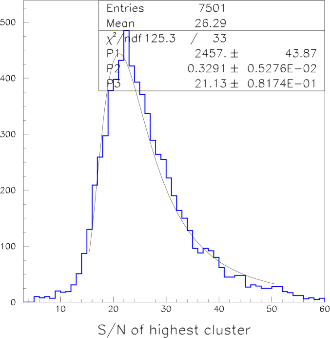
To test the TOB modules with real particles, a cosmic test stand has been
realized. With this setup a S/N of 26 is measured in deconvolution mode.
For faster measurements, important during the mass production phase, the
modules are exposed to a Ru -source, which provides
electrons with a maximal energy of 3.5 MeV and a trigger rate of 500 Hz.
For electrons, the S/N is typically 33 in peak mode
and 21 in deconvolution mode (Fig. 5). The
difference in S/N for cosmic muons and
electrons is mainly due to the different mean path lengths in the silicon.
The double-sided modules have been exploited
to calculate the hit efficiency, which is found to be as high as
99.8 %. First tracking and alignment studies at the overlap of two
double-sided modules were already carried out.
3 Conclusions
The system tests of the TEC, TIB and TOB subdetectors of the CMS silicon strip tracker are in an advanced state. Increasingly more complex substructures are being integrated and studied in laboratory system tests as well as in test beam experiments. Up to now the design has been proven to work very well, exhibiting low noise and excellent signal-to-noise ratio performance. In the TEC system test a full petal will be integrated until the end of the year, while for the TIB the next step is the integration of four full single-sided strings. Mass production of silicon strip modules has started, and the first fully equipped substructures will be installed on the disk and barrel structures in the first half of 2004.
References
- [1] M. Angarano for the CMS Tracker Coll., Nucl. Instrum. Meth. A501, 93 (2003).
- [2] L. Borello, E. Focardi, A. Macchiolo, A. Messineo, Sensor design for the CMS Silicon Strip Tracker, CMS Note 2003/020 (2003).
- [3] G. Cervelli et al., Nucl. Instrum. Meth. A466, 359 (2001).
- [4] J. Troska et al., IEEE Trans. Nucl. Sci. 50, 1067 (2003).
- [5] J.A. Coughlan, Proc. of the Workshop on electronics for LHC experiments, Colmar, 296 (2002).
- [6] C. Ljuslin, M. Marchioro, C. Paillard, Proc. of the Workshop on electronics for LHC experiments, Colmar, 174 (2002).
- [7] S. Baird et al., IEEE Trans. Nucl. Sci. 47, 158 (2000).
- [8] The CMS TriDAS Coll., Proc. of the International Conference on Computing in High Energy and Nuclear Physics, Beijing, 601 (2001).
- [9] M. Gulmini et al., Proc. of CHEP 03, eConf C0303241:THGT002 (2003).
- [10] B.G. Taylor for the RD12 Coll., IEEE Trans. Nucl. Sci. 45, 821 (1998).