Surface Analysis of OFE-Copper X-Band Accelerating Structures and Possible Correlation to RF Breakdown Events
Abstract
X-band accelerator structures meeting the Next Linear Collider (NLC) design requirements have been found to suffer vacuum surface damage caused by radio frequency (RF) breakdown, when processed to high electric-field gradients. Improved understanding of these breakdown events is desirable for the development of structure designs, fabrication procedures, and processing techniques that minimize structure damage. RF reflected wave analysis and acoustic sensor pickup have provided breakdowns localization in RF structures [1] [2]. Particle contaminations found following clean autopsy of four RF-processed travelling wave structures, have been catalogued and analyzed. Their influence on RF breakdown, as well as that of several other material-based properties, will be discussed.
1 Introduction
RF breakdown rates in Next Linear Collider (NLC) X-band (11.424 GHz) travelling wave structures currently exceed the design limits (i.e. one breakdown per 10 hours at an electric field of 65MV/m with a 400ns pulse length). In addition to excessive breakdown rates, a high degree of variability in performance among identically manufactured and processed RF structures has been observed.
In the late 1990s NLC structure prototype testing began with the availability of more powerful RF sources; initial tests revealed catastrophic RF breakdown surface damage and phase shift (detuning) beginning at an average gradient of 50MV/m [3] [4]. As RF breakdown performance has become one of several critical factors defining the limit of the operating gradient of an accelerating structure, greater efforts have been made in characterizing, understanding, and reducing RF breakdowns. A key question which needs to be addressed in depth is the limiting factors on the use of copper as an accelerator material, as accelerating gradients move toward 100MV/m.
This paper explores the possible correlation between the location and frequency of occurrence of breakdown events (Fig.1(a and b) and Fig.2) and their connection to copper surface morphology or contamination in travelling wave structures. The goal of this ongoing work is to identify the cause of the breakdown events and to diminish their occurrence, hence reducing operational variation among structures.
The universally accepted starting point for the initiation of RF or DC breakdown is field emission. RF breakdown events take place when the local field emission current density at a given site causes ohmic-heating sufficient to locally release gas, leading to ionization and ion back-bombardment that leads to further heating, plasma formation and, occasionally, catastrophic breakdown [5] [6].
2 Accelerator Structures
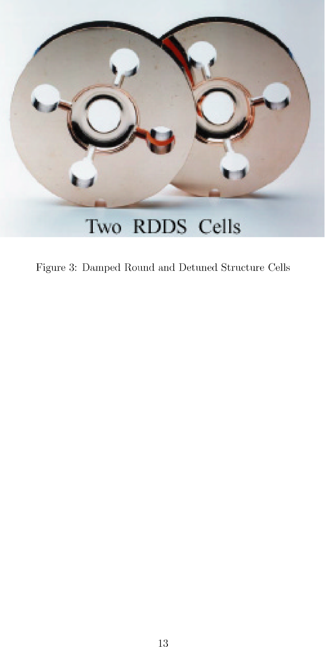
The accelerator structure is manufactured from 99.99% pure OFE copper that has been evaluated as Class 1 material per ASTM-B66. To form a cell, Fig.3, the copper is machined either with a poly- or a mono-crystal diamond tool. Chemical cleaning and etching is performed after the final machining step to remove machining-related damaged material from the surface. An iris and a half cup side forms a half cell, Fig.3. After cleaning, the two half cells are diffusion bonded together in a dry hydrogen furnace to form a full accelerator cell. Several braze cycles are required for RF couplers and water lines and a wet/dry hydrogen cleanup furnace cycle follows the brazing steps. The structure is then vacuum fired at 650oC for two weeks to outgas dissolved dissolved gases, primarily hydrogen, which can be available for breakdown plasma formation. Vacuum-firing also reduces contaminant concentration on the structure surface. Desorption of surface/bulk gas contributes to the RF breakdown mechanism [5].
Following electrical field mapping of the completed structure and installation in the NLC test accelerator, the structure is vacuum-baked, in-situ, for approximately one week prior to RF processing. RF processing is required to “season” the structure – remove large particle contaminants, desorb gas from the surface and vaporize any asperities by field emission. RF processing takes place as a series of increasing pulse lengths and energies until breakdown events at the desired operational gradient and pulse duration cease. The objective of processing is to apply sufficient power to physically alter potential field emitters without causing damage, manifested as a phase shift, to the structure surface. A typical RF processing procedure is as follows: Initial processing takes place with 50ns pulses and the gradient is increased to 70 – 75 MV/m. Once the structure operates without frequent breakdown at that pulse width, the pulses are increased in length – 100, 170, 240, and finally 400ns. After increasing the pulse length the gradient is reset to a lower value and increased until consistent RF performance is achieved at 75MV/m. Table 1 shows the variation in RF Breakdown performance, for a steady operation, among several structures at a lower gradient than the maximum gradient achieved. RF processing times for similar structures have varied as much as an order of magnitude with the range 100 to 1000 hours. Structures that take less time to process tend to have better final performance (fewer RF breakdowns.) This suggests two possibilities: (1) Structures that required less RF processing had fewer mechanical defects or surface/bulk contaminations responsible for field emission or, (2) structures that require longer processing times (due to outgassing or contamination) undergo material changes that can subsequently produce field emitters during operation.
3 RF Breakdown Measurements and Structure Autopsy
During catastrophic RF breakdown events, RF transmitted energy is negligible [7]. Energy is partially reflected and partially absorbed by the material surface. Hence, breakdown events can be characterized by changes in the reflected RF power. Approximate breakdown position in the structure is calculated by the measurement of the the phase and timing of the reflected signal. A complementary acoustic detection method, which takes advantage of the conversion of the breakdown energy into phonons, is also used to localize the breakdown events [1].
RF-processed sections were cleanly autopsied (sectioned without adding chemical contamination or physical debris). Scanning electron microscopy (SEM) was used to obtain topographical images of the surface and electron dispersive spectroscopy (EDS) was used to determine the chemical composition of the surface and any particle(s) that may be on or embedded into the surface.
Particle analysis was performed using ZepTM automated searching software from ASPEXLLC. Four strips per cell side, each oriented azimuthally 90∘ apart and having 1.4 mm width by 4.3 mm radial length from the edge of the iris, were searched. Search conditions were set for feature size and chemical composition. Any feature, which met the search criteria, was detected by backscattered electrons during an initial survey of the surface, then automatically magnified and imaged at 500x using secondary electrons. Each imaged particle was also analyzed by EDS.
4 RF Breakdown in Travelling Wave Structures: Observations
The site for enhanced field emission is some type of surface feature, either intrinsic (grain boundaries, cracks, inclusions, slip lines) or extrinsic (contamination particles, oxides, organic residues). Contaminants, inclusions, and residues can be metal or dielectric (field emission enhancement is known to occur, via separate mechanisms, in both types of material.)
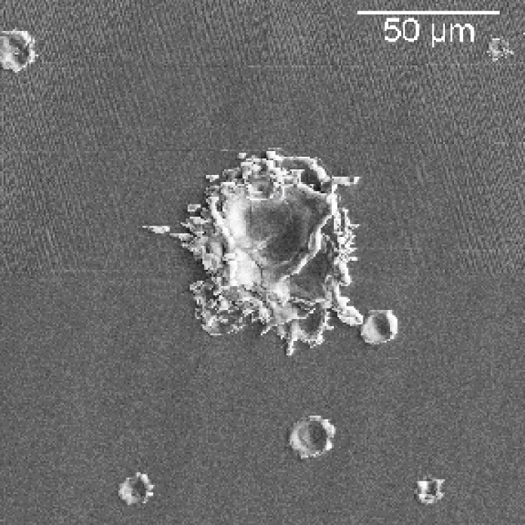
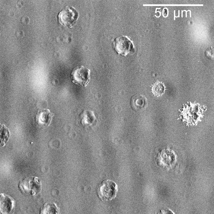
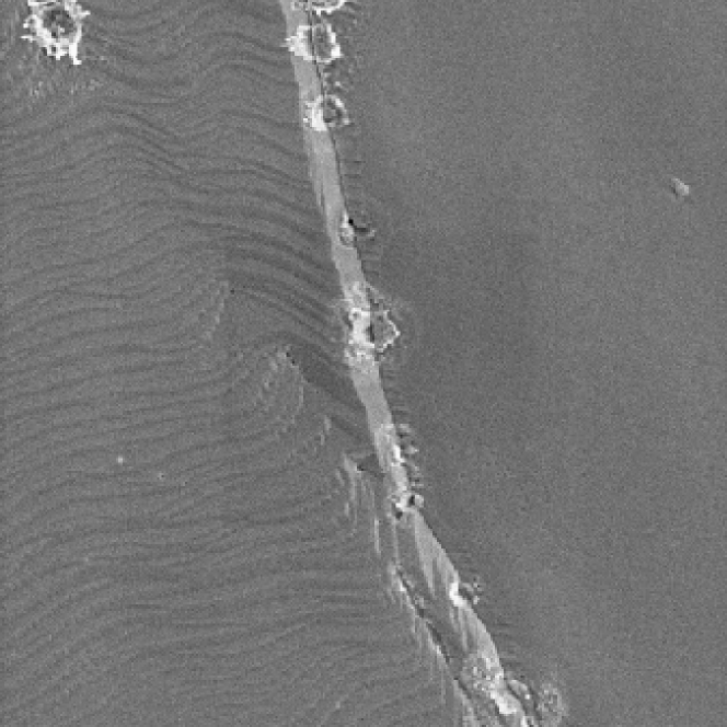
The defect dissipates some of the RF energy. Melting at the breakdown site creates craters that, due to their irregular geometry, can act as further sites for enhanced field emission and breakdown. The observed physical morphology of the craters falls into two distinct groups: irregular edges and softened edges. Fig.1(a) shows a crater with irregular edges; in Fig.1(b) a second type of crater is observed where there are few sharp edges and repeated melting appears to have taken place. The softened-edge craters often appear in close proximity with one another; irregularly edged craters are frequently spaced further apart. This suggests that the softened-edged craters may have started out irregularly edged, but have changed morphology due to repeated melting or plasma-ion bombardment.
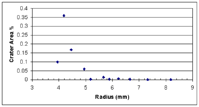
In general the density of craters increases along the cell radius toward the center, where electric fields (E) are highest, Fig.2. It is important to note that not every grain near the aperture exhibited craters and that the crater density varied substantially from grain to grain.
Craters were also seen at grain boundaries and at inclusions, Fig.4. Grain boundaries and inclusions are logical field emitters considering a Fowler-Nordheim model, equation.1. Both of these defect types have irregular geometries that increase the value of (field-enhancement factor); simultaneously these defects indicate an area of high stress within the material, which could decrease the work function , increasing the field emission:
| (1) |
Changes in work function could explain the occurrence of RF breakdown without the characteristic sharp edges and/or tall asperities typically associated with high . Preliminary measurements of the local energy barrier height of the surface of (111) OFE Copper via UHV-STM by Mizuno [8] reveal a value of 4.1eV, 18% less than macroscopic work function value of 5.0eV.
Of particular interest is the role of copper surface plasticity in RF breakdown. Local heating, as well as the presence of high magnetic and electric fields, are known to create mass movement in copper [9]. Inclusions emerging at grain boundaries and microprotrusions (slip lines), created by local stresses due to mass movement, can act as field emitters. So, there can be a sufficiently high field or local heating that could induce mass movement in copper, thus resulting in RF breakdown. Fig.4 does present mass movement inside a grain, and a crater with no traces of contaminant. However, we have not correlated systematic mass movement in a grain with breakdown events.
Mechanical deformation is known to change the local work function in copper [10]. This change in work function may enhance Fowler-Nordheim field emission without increasing .
5 T-Series Structure Autopsies: Input Coupler Design and Anomalous Chemistry
The first autopsies and SEM/EDS analysis took place on two test structures, T53VG3R and T53VG3RA. The structures were nearly identically manufactured; their difference being the final chemical cleaning step. Prior to assembly, parts of the R-structure were etched for 60 seconds; the RA-structure parts were etched for 30 seconds. This corresponds to the removal of 3 microns and 1.5 microns of surface material, respectively [11]. The etch step removes material damaged by machining, to some extent. The RA breakdown rate was twice that of the R structure in the interior cells and 7 times greater when including the breakdown attributed to the input coupler, Table 1.
Both structures exhibited high breakdown rates in their very first cells due to breakdown events in the RF input coupler [12]. The input coupler design had sharp corners that amplified local heating and has since been redesigned. It is speculated that breakdown events in the input coupler create a shower of particles that travel into the structure and created more breakdown events in subsequent cells. Breakdown rates in the center cells of the structures were significantly lower.
SEM autopsies of input, center, and output cells revealed numerous craters. Craters were located at grain boundaries and in the interior part of the grain. Inclusions were also observed. The inclusions were metal-sulfide particles, particularly manganese sulfide (MnS). The high number of MnS particles found in both T53VG3R and RA are anomalous; the most commonly found particles are copper, furnace insulation (silicon, calcium), aluminum, carbon, and stainless steel (iron, chromium). MnS signal was observed most frequently in cells close to the RF input coupler. Normalized particle data is listed in Table 2 and Table 3. The total area scanned per cell was 25 mm2. The average particle size in the interior cells was less than 1 micron. Particles greater than 5 microns were seen most frequently in the cell closest to the input coupler.
While greater particle counts were associated with the breakdown events at the input coupler, there was little correlation between particle density and breakdown events in a particular cell despite the occurrence of MnS clusters in some cells. No correlation was observed in autopsies of other systems.
6 H-Series Structure Autopsies: ”Hot” Cells due to Large Particles
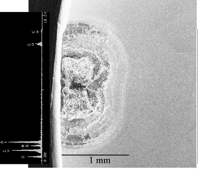
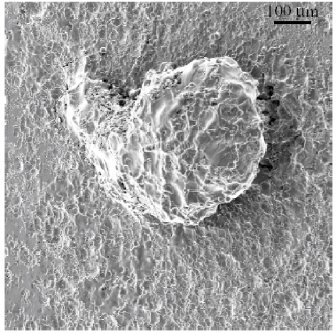
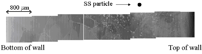
Two processed structures, H90VG5 and H90VG3N, did exhibit high RF breakdown in a localized region within the structure. At the bottom of the cell 13, between iris 12 and iris 13, of H90VG5, an aluminum sliver (mm length) was found, Fig.5. In cell 35-36 of H90VG3N a large ( 100 microns) stainless steel (S/S) particle, Fig.6 was found embedded in the sidewall of the cell. A high density of craters was found near the S/S particle, Fig.7. The aluminium sliver was likely introduced to the structure during assembly in the NLTCA. The process by which the S/S particle was introduced inside the structure is not so clear because the particle is now actually embedded into the copper.
Using RF design simulation software the intensity of the magnetic or electric field inside a structure or a cell can be determined. At the location of the cup side the magnetic field (H) of the RF wave is maximal 0.3MA/m, on the iris it can be up to 5 times less . The surface electric field on the iris is 150MV/m and is 7MV/m at the location of the S/S particle. The pattern of the melting at the base of this particle is consistent with a high current induced by H [13].
H90VG3N was fitted with a new type of input coupler having rounded edges; breakdown rates were high in cells nearest to the front of the structure. Analysis of those cells shows particle densities slightly lower than those in cells with significantly fewer breakdown events, Table 4. Following the design change, the highest number of breakdowns is concentrated at the entrance of the first accelerating cells.
7 Conclusion
The field emission from particles and defects on accelerator RF component surfaces can initiate irreversible breakdown damage in high surface electric fields. Past electron microscopical analysis of breakdowns at copper grain boundaries demonstrated the importance of a sub-surface gas source for the breakdown plasma creation, showing that vacuum bakeout of the finished structure is useful in reducing this contributor to the breakdown process.
We focused in this work on the autopsy and SEM examination of three fully RF-tested NLC structures, in order to determine whether the large number of breakdowns seen in RF structures is directly correlated with the particle load. The structure autopsies show that near clean-room technique in fabricating structures is essential to reducing gross particle loads that can lead to breakdowns. Further, careful attention must be paid to the structure vacuum bake environment in order to prevent adding non-native contamination (for example, the evaporation of manganese from the S/S vacuum components) to the last steps of structure preparation. The autopsies, however, show that most RF breakdowns have no visible particle residue or defect in the resulting craters and that most particles do not, in fact, breakdown. Therefore, most breakdown events must have some not-yet-identified cause (presumably sub-surface) for the onset of field emission. Studies of correlation between mass movement inside a grain, hardness of grains with breakdown position, and (E,H) field are ongoing.
8 Acknowledgments
We would like to thank C. Adolphsen and V. Dolgashev for useful discussion, and G. Collet for developing the clean autopsy process for structures.
References
- [1] J. Nelson et al. Use of Acoustic Emission to Diagnose Breakdown in Accelerator RF Structures. In PAC, Portland USA, 2003.
- [2] C. Adolphsen et al. Normal-Conducting RF Structure Test Facilities and Results. In PAC, Portland USA, 2003.
- [3] C. Adolphsen et al. RF Processing of X-Band Accelerator Structures at the NLCTA. In LINAC, Monterey USA, 2000.
- [4] C. Adolphsen et al. Processing studies of X-band accelerator structures at the NLCTA. In PAC, Chicago USA, 2001.
- [5] L.L Laurent. High Gradient RF Breakdown Studies. PhD thesis, University of California Davis, 2002.
- [6] P.B Wilson. Gradient Limitation in Accelerating Structures Imposed by Surface Melting. In PAC, Portland, Or, USA, 2003.
- [7] V. Dolgashev. Experiments on Gradient Limits for Normal Conducting Accelerators. In LINAC 2002, Korea, 2002.
- [8] Mizuno and Garwin, SLAC private communication.
- [9] E.V Vorob’ev. Deformation of Copper under the Action of Strong Magnetic Fields and Cryogenic Temperatures. Problemy Prochnosti, 21(12):32–36, 1989.
- [10] Chow and Tiller. Deformation-Induced Work Function Changes in Cu Single Crystals I. Experiment. J. Appl. Phys., 55(5):1339, 1984.
- [11] R.E. Kirby et al. Impact of Surface Preparation on RF Breakdown Performance in NLCTA Accelerating Structures. Technical report, SLAC LCC-0081, 2002.
- [12] F. Le Pimpec et al. Autopsy on an RF-Processed X-band Travelling Wave Structure. In LINAC 2002, Korea, 2002. SLAC-PUB-9526 .
- [13] V. Dolgashev, SLAC private communication.