Blending of nanoscale and microscale in uniform large–area sculptured thin–film architectures
Mark W. Horn, Matthew D. Pickett, Russell Messier and Akhlesh Lakhtakia111Corresponding author. Tel: +1 814 863 4319; Fax: +1 814 865 9974; E–mail: AXL4@psu.edu
Department of Engineering Science & Mechanics,
Pennsylvania State University,
University Park, PA 16802–6812, USA
Abstract
The combination of large thickness ( m), large–area uniformity
(75 mm diameter), high growth rate (up to 0.4 m/min) in
assemblies of complex–shaped nanowires on lithographically
defined patterns has been achieved for the first time. The nanoscale and the microscale
have thus been blended together in sculptured thin films with transverse architectures.
SiOx () nanowires were grown by electron–beam evaporation onto
silicon substrates both with and without photoresist lines (1–D arrays) and checkerboard
(2–D arrays) patterns. Atomic self–shadowing due to oblique–angle deposition enables
the nanowires to grow continuously, to change direction abruptly, and to maintain
constant cross–sectional diameter. The selective growth of nanowire assemblies on
the top surfaces of both 1–D and 2–D arrays can be understood and predicted
using simple geometrical shadowing equations.
PACS: 81.16.-c, 81.15.Ef, 81.16.Rf
Keywords: nanofabrication, nanoscale pattern forming, sculptured thin film, vacuum deposition
1 Introduction
Raise the temperature and lower the pressure sufficiently, and virtually any solid material shall begin to evaporate. Condense the directional vapor on a substrate at a temperature less than about a third of its melting point, and you will obtain a columnar thin film with column diameters on the order of tens of nanometers. The technology of columnar thin films (CTFs) was born in 1885, when Kundt collected the vapor from a solid on a substrate held at an oblique angle to the incident, directed vapor flux [1]. Even before the commercial advent of transmission electron microscopes (TEM) in the 1950 s and scanning electron microscopes (SEM) in the 1960 s, it was known from optical experiments that such films are anisotropic [2] — not unlike crystals. However, unlike the anisotropy of crystal structures, the anisotropy of CTFs is morphological: Self–shadowing at the atomic level [3] leads to parallel columns growing towards the obliquely incident vapor flux, albeit at an angle to the average direction [4]. TEMs and SEMs eventually provided visual evidence of the nm–scale morphology of CTFs grown by oblique–angle deposition [5], thereby confirming the optical analogy with crystals.
Also unlike crystals, the separated and slanted nanocolumns (currently termed nanowires) can be shaped during growth by substrate motion [6]. Elementary experiments were reported by (i) Young and Kowal in 1959 [7] who rotated the substrate about an axis passing normally through it, and (ii) Nieuwenhuizen and Haanstra in 1966 [5] who altered the substrate tilt with respect to the average direction of the incident vapor flux once during deposition. The products of these experiments were the precursors of sculptured thin films (STFs) developed during the last decade [6], chiefly for optical but also other applications [8].
STFs are assemblies of parallel, shaped nanowires that can be fabricated by design using physical vapor deposition techniques, such as thermal and arc evaporation, sputtering, and pulsed laser ablation [4, 8, 9, 10]. As the nanostructure comprises multimolecular clusters of 3–5 nm diameter, rapid changes in the average direction of the incident vapor flux relative to the substrate lead to the growth of parallel nanowires of curvilinear shapes. At infrared, visible and lower ultraviolet wavelengths, the assembly of nanowires can be effectively considered as a continuous anisotropic medium whose electromagnetic response properties are inhomogeneous normal to the substrate [11] — which allows the exploitation of commonplace design techniques for devices such as optical polarizers, filters and sensors [8, 9].
The STFs fabricated thus far possess, for the most part, simple transverse architectures, as the constituent nanowires are randomly nucleated on the substrate. The film growth rates can also be low, depending on the deposition method employed, due to the large oblique angles during deposition. Furthermore, the transverse area rarely exceeds 1 cm 1 cm without significant loss of transverse uniformity. These three factors have stymied the economic exploitation of STFs, despite the theoretical design and experimental realization of many STF–based optical devices [8, 9]. Fabrication of complex STFs of large transverse area and at high deposition rates would increase the economic attraction of STFs.
We present here a newly realized technique to economically grow thick, uniform, large–area STFs with transverse architectures that blend the nanoscale and the microscale. Our work goes beyond initial work on patterned growth in thin films [12]–[14] in that we examine different microscale architectures employing a range of feature sizes and shapes with controlled depth and shape of topography, and have achieved this over relatively large ( mm dia) areas.
We have chosen to illustrate the growth of sculptured nanowire assemblies by examining the deposition of SiOx, a dielectric substance, on substrates photolithographically patterned with posts, holes, and various densities of lines and spaces that were generated using a deep ultraviolet (DUV) stepper. Although we have examined the deposition of several materials (such as SnO2, Mo, Cr and Al) in addition to SiOx, for the sake of brevity we only show examples of SiOx films deposited at a single angle of vapor–flux incidence. We continue to investigate STFs grown at various oblique angles of vapor–flux incidence, deposition rates, and substrate rotational velocities in order to better understand how the initial topography of the substrate affects the growth and expansion of nanowires.
2 Experimental
A 10–kW dual electron–gun evaporator was used to obliquely deposit material on either fixed or rotating substrates, as shown schematically in Fig. 1a and b. The system was cryopumped to a base pressure of Torr. A 100–cc, 50–mm diameter crucible was charged with pellets of SiO2 before each deposition. Deposition rates were measured using a quartz crystal monitor (QCM) held perpendicular to the vapor flux. The measured deposition rate depends on the mass density of the vapor flux, and is quite different from the film growth rate defined as the rate of increase of film thickness. Deposition rates from 54 to 480 nm/min were measured, while the film growth rates varied between 100 and 1000 nm/min. Nanowire shapes were controlled via computer, and substrate rotational velocities ranged from 0.5 to 36 rpm.
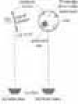
The throw distance to the center of the rotating substrate was 250 mm, and the center of the wafer was nominally positioned directly above the center of the crucible; see Fig. 1a. Unlike previous work, the electron beam in our system was rastered over a large portion of the crucible, and the flux produced more closely resembles a uniform flat source, analogous to a plane wave in electromagnetics textbooks [15], than a point source. Furthermore, the mean free path during deposition was much greater than the source–to–substrate distance, leading to line–of–sight deposition. Thus, the arriving vapor flux is highly directed, thereby eliminating the need for collimation. For example, we observed uniformity of thickness and morphology of complex sculptured nanowires across the diameter of a 75 mm substrate. However, highly directed vapor flux leads to significant local nonuniformity due to shadowing effects for oblique incidence on non–planar (i.e., patterned) substrates.
The substrates upon which the sculptured nanowire assemblies were deposited consisted of a 1 cm 1 cm die of a silicon wafer patterned with a photoresist stack placed on top of and near the outer edge of a 75 mm silicon wafer, as shown schematically in Fig. 1b. The substrates were clipped into place on a rotating substrate holder driven by an external stepper motor via a rotary vacuum feed–through. For all films presented in this paper, the vapor flux was directed at an angle to the substrate plane.
The photoresist features shown throughout this paper were generated using a resolution test mask and a DUV (248 nm) stepper. A Shipley UV5 photoresist was applied to a 150 mm silicon wafer coated with a Shipley lift–off photoresist (LOR) layer. The two–layer photoresist stack — used to facilitate selective removal of a deposited film — was then exposed, baked after exposure, and then developed to yield a wide variety of 1–D and 2–D features from 0.4 m to hundreds of microns wide and 0.8 m high with nearly vertical sidewalls. After deposition, the films were cleaved into smaller pieces and were analyzed in cross–section using a LEO 1530 field emission SEM (FESEM), usually at voltages between 2 and 5 kV to minimize charging of the dielectric nanowires.
3 Results
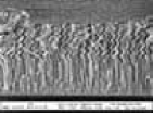
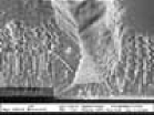
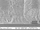
Figures 2a and b are cross–sectional SEM micrographs of a two–section STF comprising helical (chiral) nanowires and chevronic (nematic) nanowires grown sequentially, without stopping the evaporation process. A flat silicon wafer with no photoresist pattern was used. The substrate revolution rate for the chiral section (with 3–D morphology) of the STF was 4 rpm. The nematic section (with 2–D morphology) of the STF went through nine rapid changes of the substrate tilt ( to with respect to the normal to the substrate), one change every 30 s. The deposition rate was fixed at 120 nm/min. The total height (i.e., thickness) of the film, as measured using the SEM micrographs, is approximately 4 m. The total deposition time was 10 min, yielding an average growth rate of 400 nm/min. Fig. 2a shows a total cross–section of the film, whereas Fig. 2b shows a high magnification of the region where the film abruptly, yet continuously, transitions from the chiral section to the nematic section.
(a) (b)
Figures 3a and b are cross–sectional SEM micrographs of a two–section STF taken at the center and edge, respectively, of a 75 mm substrate cleaved along its diameter. This 2–section chiral STF was grown by varying the deposition rate while holding the substrate rotational velocity fixed at approximately 2 rpm. The deposition rate was set at 54 nm/min for the first section, and increased to about 300 nm/min for the second section. The structure and density of the nanowires are very similar in both micrographs, even though the center of the substrate must receive a relatively constant vapor flux during an entire revolution while the edge must experience some variation. In our deposition chamber, if there was a large variation in deposition rate either from the bottom to the top of the substrate or from the left to the right of the substrate (see Fig. 1a), a significant variation in the chiral morphology of the nanowires should be expected. However, at least at the nanoscale, we see very little difference in the nanowire assemblies deposited at the edge of a 75 mm rotating substrate with those grown at its center, which is consistent with our assumption that the wide melt pool in the crucible is acting more like a planar deposition source than a point source.
(a) (b)
Figures 4a and b are cross–sectional SEM micrographs of a yet another different STF taken at the center and an edge, respectively, of a 75 mm dia silicon substrate. This 2–section film was grown by fixing the deposition rate at 120 nm/min and abruptly changing the substrate rotation velocity from 1 to 36 rpm. Notice again the similarity in morphology in the two different cross–sections, confirming the high degree of uniformity of deposition across large areas. Also notice that, as the substrate rotational velocity is increased, the helical shape of the individual nanowires is lost and larger diameter nanocylinders grow orthogonal to the substrate surface.
(a) (b)
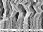
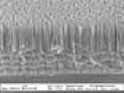
Figure 5 is a cross–sectional SEM micrograph of a STF grown simultaneously with the two–section STF of Fig. 2, except that the former was deposited on a photoresist–patterned substrate. The micrograph in Fig. 5 shows the growth behavior at a single 1–D topographical step. The nanowire assembly in the left portion of Fig. 5 grew on top of the 0.8–m high photoresist and is morphologically similar to the STF of Fig. 2. Likewise, the morphology of the nanowire assembly on the far right of Fig. 5, well away from the step, is essentially the same. In all these cases there is no shadowing due to the substrate; only self–shadowing occurs at the atomic level that leads to the growth of individual nanowires. The film that grows on the side of the photoresist step appears much denser and devoid of distinct nanowires. However, zone 1 (see Fig. 5) shows indications of layered, shadowed–growth during the 3–D chiral–section growth, and zone 4 displays oblique columnar shadowed-growth related to the 2–D nematic section. Zones 2 and 3, farther away from the shadowing ledge, have the appearance of chiral section. The shadowing distance of a 0.8–m high step is about 3 m to the right of the step (zone 2), followed by about a 1 m transition region (zone 3) to the un-shadowed region on the right of the micrograph.
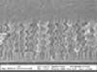
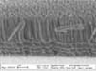
The STF of Fig. 3 was also grown on a patterned–die substrate with 1.5–m–wide and 0.8–m–high photoresist lines. Figures 6a and b provide cross–sectional SEM micrographs of this film. In Fig. 6a, we have focused on the morphology developed over a single line. Shadowing by the 1–D topography is evident on both sides of the line. To the left of the line, the shadowed–morphology zones are similar to those in Fig. 5. At a distance far enough to the left of the line such that no shadowing occurs, the morphology and thickness of the STF on the flat Si substrate are the same as that grown on top of the photoresist line. In the center of the micrograph, but still to the left of photoresist line, the film is noticeably thinner due to shadowing by the line, but it exhibits a similar chiral morphology. Near the line, the shadow–related morphology can be divided into several zones. Zone 1 is related to shadowed–growth on the line s sidewall, while zone 2 is shadowed–growth emanating from the Si substrate. The boundary between these two zones appears to follow a power–law growth evolution that results from competition between growths on the sidewall and the bottom surface [4]. The boundary between zone 2 and the transition zone 3 (at about 4 m from the left sidewall of the line) is less abrupt than in Fig. 5 (where the upper section is of the nematic type in which the shadowing effects are more significant, as discussed in the next section). The unshadowed–growth at the left is almost 5.5 m from the left sidewall of the line.
The very thin layer at the far right of the micrograph in Fig. 6a is shadow–related growth onto an adjacent space between two photoresist lines with sidewall separation of 1.5 m; see Fig. 6b. A thin but visible coating grew on the sidewalls and the bottom of both 1.5–m–wide spaces between adjacent photoresist lines. A lower magnification, edge–on view of this film is provided in Fig. 7a.
(a) (b)
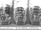
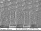
Figures 7a–c are additional cross–sectional SEM micrographs of the same sample as shown in Fig. 6, but taken edge–on at different locations along a 1–D array of photoresist lines. Fig. 7a focuses on growth on two sets of three lines. The lines and the spaces between them are 1.5 m in the left set, and 1.4 m in the right set. A 3–m–separation between the two sets allows for shadow–growth comparisons for systematically varied shadow geometries. The lower growth between the lines in a particular set is in contrast to the higher growth between the two sets. Sets of lines with decreasing linewidths and spacewidths are seen in Figs. 7b and c: going from left to right, the widths decrease from 0.8 to 0.6 m in Fig. 7b, and from 0.6 to 0.4 m in Fig. 7. There is no observable growth in the spaces of smaller widths, and very little growth on the sidewalls.
Larger separations of 3.5 m (Fig. 7c) and 4.5 m (Fig. 7b) can be seen between adjacent sets of lines. In these regions, growth on the bottom and on the sidewalls increases in direct proportion to the sidewall–to–sidewall separation. Nanowire arrays on the middle line of each set undergo an initial stage of lateral expansion, originating at the photoresist corners and sidewalls, followed by a steady–state vertical growth. The nanowire arrays on the middle lines maintain a nearly constant separation from the respective outer lines for most of the 3.2–m thickness of the film, with only slight rounding at the top edges. Also notice how this separation distance decreases with the spacing between the photoresist lines.
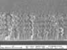
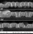
Figures 8a–c are cross–sectional SEM micrographs of increasing magnification, showing the same two–section film described in Figs. 3, 6, and 7, except that this portion of the film was grown on a checkerboard pattern (2–D array) of photoresist. The checkerboard dimensions are 1.5 m 1.5 m steps and wells. The chiral nanowires are selectively deposited on top of the topographic features with no deposition occurring between the features, which is evident from Fig. 8c. Thus, 2–D arrays of nanowire assemblies can be deposited over large areas (Fig. 8a), with good uniformity (Fig. 8b), and with nearly vertical sidewalls (Fig. 8c).
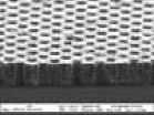
(a) (b)
(c)
4 Discussion
The combination of large thickness ( m), large–area uniformity (75 mm diameter), high growth rate (up to 0.4 m/min) STFs with complex nanowire shapes (Figs. 2–4) on lithographically defined patterns (Figs. 5–8) has been achieved for the first time. Atomic self–shadowing due to oblique–angle deposition (at from the substrate normal, ) enables the nanowires to grow continuously, to change direction abruptly, and to maintain constant cross–section, as seen in Fig. 2. By controlling the longer–range–shadowing of the collimated, directed vapor flux by the photoresist pattern geometries, it has become possible to grow STFs selectively on the top surfaces of both 1–D lines (Figs. 6 and 7) and 2–D checkerboard arrays (Fig. 8). The selectivity, as indicated by growth on the sidewalls of the photoresist features and the bare bottom surfaces, is directly related to the feature spacing which, in turn, is related to the geometrical shadowing distances.
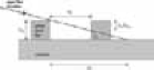
The various morphological features of the STFs emanating from the photoresist sidewalls and the bottom (silicon) surfaces, as noted and described in the last section, can be understood in terms of simple geometrical shadowing. The shadowing distance of a surface feature of sidewall height due to an oblique angle flux, as shown in Fig. 9, is given by
| (1) |
where is a geometrical factor and is the angle between the average direction of the vapor flux and the substrate plane. This equation has been applied to atomic–level self–shadowing [4] and applies equally well to the sculptured nanowire assemblies presented here. As and m for all films in Figs. 2–8, . Therefore, the shadowing distance when the vapor direction is perpendicular to the feature (e.g., photoresist line) is m. This only describes shadowing of the bottom surface perpendicularly adjacent to the sidewall of a m–high feature, as in the case of 2–D nematic growth. If the separation of the features is less than , the growth on the sidewall of an adjacent feature (see Fig. 9) will coat only a fraction of the sidewall from the top down; accordingly,
| (2) |
where is the distance between the feature ledges. For small feature separations, as studied here (see Figs. 7 and 8), is much smaller than unity.
With this simplistic model of shadowing behavior, it is possible to understand the morphologies obtained in this study. In Fig. 5, for a single step where shadowing occurs only from one direction, the width of zone 2 (deposition on the bottom surface) is about 3 m which is close to the shadowing distance. The morphology at the bottom on the left shows columns slanted upward to the right in the direction where the vapor is arriving unshadowed. On the right side of zone 2, the columns becomes more vertical, likely the result of shadowing from the faster growing film on the far right that is growing un-shadowed in all directions. The transition zone 3 appears to be related to the dynamic shadowing effects coupled with the change of deposition from multidirectional (chiral) to bidirectional (chevronic) at which point the shadowing geometry is that shown in Fig. 9. Similar arguments can be made for understanding the morphology in Fig. 6a, though the transition from the shadowed to unshadowed zones is more gradual, likely due to the multidirectional growth during the complete film deposition.
However, for many envisioned applications deposition will be desired only on the top surface of a lithographically defined pattern. This means that no vapor arrives at the bottom surface, as in the case of nematic growth in the top section of the film in Fig. 5, as well as for chiral growth on submicron–wide 1–D line arrays (Figs. 7b and 7c) and 1.5 m 1.5 m 2–D checkerboard arrays (Fig. 8). In general, the selectivity of growth on the top surface versus growth on the sidewalls or bottom surfaces for different pattern geometries and deposition sequences can be predicted. For instance, if is increased or is decreased, a decrease in could be calculated for compensation.
The shadowing geometry gets more complicated when the vapor flux is not temporally unidirectional (inherent in the piecewise bidirectionality needed for growing chevronic nanowires), but multidirectional (as for growing chiral nanowires). In the latter case as the substrate rotates relative to the average direction of the incident vapor flux, growth will occur down the spaces between adjacent photoresist lines casting an incident vapor flux that varies in angle and in position on the side–wall and bottom surface. For substrate rotation at a constant angular velocity, as we undertook, the morphology of the deposited film will vary. More detailed mathematical descriptions and/or simulations of this complex growth will be needed if deposition in the channels between features is important. Furthermore, such a quantitative description will have to incorporate the dynamic effects of the advancing film growth–front in all directions.
The experimental evidence in Fig. 7 shows that the growth at the bottom surfaces between various 1–D arrays of photoresist lines (spaced 4.5, 3.5, 1.5, 1.4, 0.8, 0.6, 0.5, and 0.4 m apart) decreased from about 25 of the unshadowed thickness of the 4.5–m–spacing (Fig. 7b), to about 12 for the 1.5–m–spacing (Fig. 7a), and to essentially zero thickness for sidewall–to–sidewall separations of 0.8 m and less (Figs. 7b and 7c). For the 2–D checkerboard array with 1.5 m 1.5 m 0.8 m shadowed wells (Fig. 8), there is no visible growth on the bottom surface, since the largest value of is m along the checkerboard diagonal direction, which leads to . Thus, the growth will be just of the sidewall growth in the worst case, with no growth predicted on the bottom surface. The sidewall growth leads to initial expansion of the nanowire assemblies (see Fig. 8c), followed by parallel, vertical growth, once the separation is about 1 m. As the separation changes, so does the shadowing geometry. Therefore, the selectivity of growth on the pattern’s top surface will improve as is reduced and/or is decreased.
5 Concluding Remarks
We have reported the fabrication of films comprising assemblies of sculptured SiOx nanowires grown on lithographically patterned substrates, thereby incorporating transverse architectures uniformly over large–area substrates in STF technology. The density and morphology of the nanowire assemblies is dependent on the direction of the vapor flux and the local self–shadowing environment, according to straightforward geometrical considerations. We have shown that chiral nanowires can be selectively grown on patterned substrates. The spacing of the array where selective growth is achievable is determined by the direction of the vapor flux angle and the height of the initial (i.e., substrate) topography. The ability to sculpture the nanowires out of any material which can easily be deposited by a physical vapor deposition technique — coupled with micro-and macroscale 1– and 2–dimensional topographic substrates — opens a whole new realm of photonic, fluidic and sensor devices [8, 9, 10, 11, 17]. Such applications include nanowire assemblies for bionanotechnology [18, 19], as well as for photonic bandgap engineering [20].
Acknowledgement This work was supported in part by the Penn State Materials Research Science and Engineering Center.
References
- [1] Kundt A 1886 Ueber Doppelbrechung des Lichtes in Metallschichten, welche durch Zerstäuben einer Kathode hergestellt sind Ann. Phys. Chem. Lpz. 27 59
- [2] Hodgkinson I J and Wu Q h 1998 Birefringent Thin Films and Polarizing Elements, World Scientific, Singapore
- [3] König H and Helwig G 1950 Über die Struktur schräg aufgedampfter Schichten und ihr Einfluß auf die Entwicklung submikroskopischer Oberflächenrauhigkeiten Optik 6 111
- [4] Messier R, Venugopal V C and Sunal P D 2000 Origin and evolution of sculptured thin films J. Vac Sci. Technol. A 18 1538
- [5] Nieuwenhuizen J M and Haanstra H B 1966 Microfractography of thin films Philips Tech. Rev. 27 87
- [6] Lakhtakia A and Messier R 1994 The key to a thin film HBM: the Motohiro–Taga interface Proceedings of Chiral ’94 (eds Mariotte F and Parneix J–P.), CEA/CESTA & PIOM/ENSCPB, Bordeaux, France, 125
- [7] Young N O and Kowal J 1959 Optically active fluorite films Nature 183 104
- [8] Lakhtakia A 2002 Sculptured thin films: accomplishments and emerging uses Mater. Sci. Engg. C 19 427
- [9] Hodgkinson I J and Wu Q h 2001 Inorganic chiral optical materials Adv. Mater. 13 889
- [10] Suzuki M and Taga Y 2001 Integrated sculptured thin films Jap. J. Appl. Phys. (Pt. 2) 40 L358
- [11] Lakhtakia A et al 2001 Sculptured–thin–film spectral holes for optical sensing of fluids Opt. Commun. 194 33
- [12] Malac M et al 1999 Fabrication of submicrometer regular arrays of pillars and helices J. Vac. Sci. Technol. B 17 2671
- [13] Malac M and Egerton R F 2001 Thin–film regular–array structures with 10–100 nm repeat distance Nanotechnology 12 11
- [14] Dick B, Brett M J and Smy T 2003 Controlled growth of periodic pillars by glancing angle deposition J. Vac. Sci. Technol. B 21 23
- [15] Chen H C 1983 Theory of Electromagnetic Waves, McGraw–Hill, New York, NY, USA
- [16] Lakhtakia A and Messier R 2003 The past, the present, and the future of sculptured thin films Introduction to Complex Mediums for Electromagnetics and Optics (eds Weiglhofer W S and Lakhtakia A), SPIE Press, Bellingham, WA, USA, 447
- [17] Kennedy S R et al 2002 Fabrication of tetragonal square spiral photonic crystals Nano Lett. 2 59
- [18] Wilkinson C D et al 2002 The use of materials patterned on a nano– and micro–metric scale in cellular engineering Mater. Sci. Eng. C 19 263
- [19] Cao H et al 2002 Gradient nanostructures for interfacing microfluidics and nanofluidics Appl. Phys. Lett. 81 3058
- [20] Pendry J B 1996 Calculating photonic band structure J. Phys.: Condens. Matter 8 1085