Microfabrication of Laser-Driven Accelerator Structures††thanks: Work supported by Department of Energy contract DE-AC03-76SF00515 (SLAC) and by DOE grant no. DE-FG03-97ER41043-II.
Abstract
We discuss the potential for using microfabrication techniques for laser-driven accelerator construction. We introduce microfabrication processes in general, and then describe our investigation of a particular trial process. We conclude by considering the issues microfabrication raises for possible future structures.
Submitted to Tenth Advanced Accelerator Concepts Workshop (AAC 2002), June 23–28, 2002, Mandalay Beach, California (AIP Conference Proceedings)
1 Introduction
Experiments to demonstrate laser-driven charged particle acceleration in vacuum have thus far relied largely on macroscopic structures, that is, structures large enough to be assembed by hand and many optical wavelengths in size. For instance, in the LEAP experiment conducted at Stanford University [1], the accelerator cell is approximately 1 cm long in each dimension compared to a laser wavelength of 800 nm, and is assembled by manually gluing together high-reflection coated quartz prisms.
Such accelerator structures are not designed to be candidates for use in a real accelerator, and indeed their capabilities are clearly not close to what would be needed in a functioning machine. For instance, the LEAP cell has a maximum accelerating gradient of 10 MeV/m, and with acceleration of 1 pC bunches over a distance of 1.5 mm using 36 µJ laser pulses at the LEAP cell, the structure has an electron-to-photon efficiency of . With just one cell, the overall wall-plug efficiency of the setup is much less, close to .
These performance parameters can be traced fundamentally to the large size of the structure; for effective accelerator cells a much smaller structure is required. Consider a laser field propagating in free space, which largely describes the field in the LEAP cell. The peak longitudinal field on axis obeys the general scaling law , where is the peak transverse field, is the wavelength, and is the transverse mode size. This relation is exact for the case of a Gaussian TEM mode, but even approximately this scaling law serves to illustrate the dependence of on the mode size. At the same time, the maximum field amplitude is fixed by the damage threshold of the optics, so higher gradients cannot be obtained by arbitrarily increasing the laser intensity. Therefore, for optimum gradient the laser mode size must be comparable to the wavelength, as is the case with RF structures.
Attaining good shunt impedance in a laser-driven structure also constrains possible designs. For reasonable efficiency a structure must accelerate particles continuously over a distance large compared to a wavelength. Therefore simply focusing a low-intensity laser pulse down to a very narrow waist to avoid optical damage will not be effective, since the small spot will diffract quickly and will not accelerate for any appreciable distance. Also, a structure may need to store laser energy for the next electron bunch. Therefore, a structure with both high gradient and good efficiency must be small, with feature sizes on the order of an optical wavelength. Fortunately, technology now exists or is rapidly being developed to fabricate such small structures, even for wavelengths in the visible or near-infrared.
2 Microfabrication Overview
We refer to microfabrication, in general, as a type of process using a set of techniques and equipment commonly used to manufacture integrated circuits (IC’s) and microelectromechanical devices (MEMS). Such a process typically starts with a bare wafer, usually of silicon. Processing of the wafer involves several types of procedures, which we describe briefly below; detailed discussions can be found in references on IC or MEMS techniques, for instance [2] or [3].
Photolithography, perhaps the most important process step, defines the structure by transferring a pattern from a mask onto an organic photoresist on the wafer surface. This is usually followed by etching, in which material is selectively removed from the wafer. Thin film deposition procedures allow many different materials to be deposited in layers on the wafer, and a thin film of SiO can be grown directly on a silicon surface by the process of thermal oxidation. Ion implantation allows dopants to be added to the structure, which diffuse through the material during subsequent high-temperature process steps. In IC manufacturing this is primarily used to control electrical properties of materials, but it can be used to control chemical and possibly optical properties as well. Chemical-mechanical polishing has recently become a common procedure for planarizing the topography of a wafer at certain points in a process. Finally, the importance of cleaning cannot be ignored. Usually involving immersion in chemical baths, each followed by a deionized water rinse, as well as adherence to cleanroom procedures, removing particulates and chemical contaminants to suppress defects is critical to IC manufacturing and will probably be equally important in accererator microstructure fabrication.
Microfabrication has great potential for accurately making small accelerator structures. Not only are highly precise procedures available now, but continued rapid improvement is driven by the extraordinary market forces in the IC industry. For instance, control of certain feature sizes is expected to reach 0.5 nm RMS by 2010 [4]. That silicon processes are so well established can be exploited for optically-driven accelerators, since silicon transmits in the telecommunications band at 1.5 µm wavelength, where many optical components are available and continue to be improved. For research purposes, there is an advanced fabrication facility at Stanford [5] where the procedures mentioned above are available. Finally, subsequent mass production using microfabrication techniques is inexpensive; this is critical since, for instance, an accelerator the length of the SLAC linac would use 10,000 300-mm wafers, the current state-of-the-art wafer size.
3 Trial Process
We have explored a trial microfabrication process for a replacement LEAP cell. While the purpose of this project was primarily to explore microfabrication procedures, it was motivated by the current LEAP cell design. As described in [1], the LEAP accelerator structure consists of two pairs of dielectric surfaces oriented at 45° to each other, with a slit in the middle for electron beam passage. Each surface has a high-reflector dielectric coating. The microfabricated cell is designed to form the e-beam slits by etching them through a silicon wafer. The etch pattern on the wafer is shown in Figure 1.
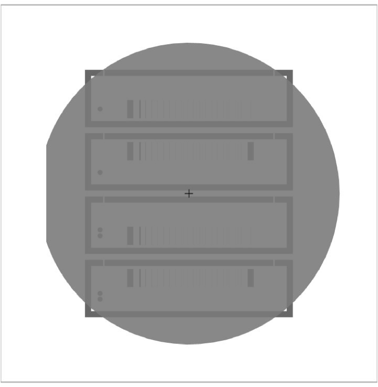
Up to four reflecting rectangles would be etched from a 4-inch wafer, and each surface would have several slits. The rectangles would then be aligned in pairs at a 45° angle. Unlike the current LEAP cell, the slits would not be individually adjustable, but there would be slits of several widths in each rectangle. In addition, having several slits would allow a new slit to be moved into place easily should one be damaged during the experiment.
The process of etching a pattern in a silicon wafer can be summarized simply as follows: We deposit layers of material on the wafer, and then selectively remove the areas to be etched from each layer, with each deposited layer protecting the regions not to be etched of the layer beneath. However, each step of the process involves a different procedure using different equipment. We now describe in some detail each step of the process.
The final step of the process will be to etch the silicon in a potassium hydroxide (KOH) solution. While the pattern will initially be imprinted in photoresist, the resist cannot be used directly to mask the KOH since the KOH will eat it away as it etches the silicon. Therefore an intermediate layer is required to mask the silicon. Silicon nitride (SiN) provides a good masking material, as it etches negligibly slowly in KOH [6]. Therefore, the first step of the process is to deposit a thin film of SiN on the silicon substrate.
We deposit a 200 nm film of SiNusing low-pressure chemical vapor deposition (LPCVD). In this procedure dichlorosilane and ammonia gases are run through a furnace containing the wafers at about 1 torr and 700\celsius. These gases react on the wafer surface to produce SiN. One hour of deposition is sufficient to give a 200 nm film.
One the nitride is deposited we spin on a layer of photoresist. This is accomplished by dropping a small puddle of the liquid resist compound on the wafer and then spinning the wafer at 3000–5000 RPM for about 60 s. After the first few seconds of spinning the resist coats the wafer uniformly; the rest of the spinning serves to dry the resist. The resist is then baked to harden it to prevent flow during the development step, discussed below.
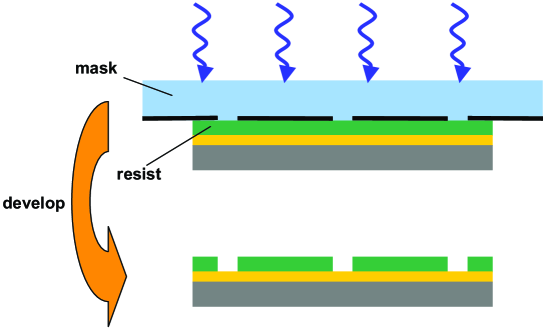
The pattern is transferred to the photoresist by placing a chome-on-glass mask over the wafer, with chrome absent from regions corresponding to etched regions on the wafer. The wafer is then brought into contact with the mask and the mask is exposed from above to 365-nm UV light from a mercury lamp. This exposes only the regions of photoresist to be removed, causing a chemical reaction in the resist. The resist compound was deliberately chosen to be thin to avoid diffraction effects; this is a concern because the slits in the mask are as thin as 1 µm. After a bake, the wafer is immersed in a developer solution, removing the exposed regions of photoresist. This procedure is shown schematically in Figure 2.
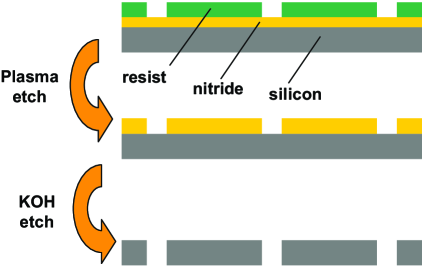
Once the photoresist is patterned, the wafer is plasma etched using CF and O gases. This removes the nitride not protected by photoresist. Once the plasma etch is complete, the resist can be removed using chemical solvents plus a quick plasma etch in O, oten called a plasma “ash,” to remove any remaining organic residues.
Finally, the wafer is etched in KOH solution. The etch is highly anisotropic, proceeding much faster in the direction than in the direction. In fact, etch ratios of greater than 600 to 1 have been obtained [6]. This is why the wafer flat in Figure 1 is oriented in the plane, and it also requires that the wafer surface be a plane. We have found that ultrasonically agitating the KOH solution improves the etch rate considerably. Once the KOH etches entirely through the wafer, the nitride can be removed using the same plasma etch used above or in a hot phosphoric acid solution, and then the optical coating can be applied. The etch process is shown schematically in Figure 3.
So far, we have obtained a 1 µm slit in the nitride coating, and etched all the way through a 500 µm-thick wafer. However, the narrowest slit we have been able to obtain is still 40–50 µm wide, and better alignment between the mask and the crystal plane will likely be able to improve upon this. The slit walls appear vertical under an optical microscope but proper observation of the structure requires an SEM scan. Depositing the dielectric coating without clogging the slits may prove difficult, especially because high-reflector coatings require many layers. As described in [2], thin film deposition geometry is highly nontrivial and an appropriate simulation would be required.
4 Microfabrication Possibilities
The use of microfabrication presents possibilities for laser-driven accelerator structures well beyond those available through bulk machining. One possibility is to use a photonic crystal structure, for instance as proposed by Lin [7]. However, the available procedures in a microfabrication process do impose constraints on the type of structure used.
The structure material must be lossless at a convenient laser wavelength, radiation hard, and the substrate material must have high thermal conductivity. Also, the structure material must be easily etched, and if the structure is made of more than one material there must be processes available to selectively etch them independently. Therefore a glass photonic crystal fiber as proposed in [7] is not viable because SiO is not radiation hard, and fibers do not release heat easily.
However, other materials may be used for a similar structure. Silicon, as mentioned above, transmits at the 1.5 µm wavelength, and is possibly is even better suited for use at a 2.5 µm wavelength. There is an immense microfabrication technology base for silicon, and it may be used as a substrate, even if it is not suited for a structure, because of its wide availability and good thermal conductivity. Quartz and sapphire are also possible materials, as is diamond. Photonic crystal structures might use these materials, and in fact a mid-infrared photonic bandgap structure has been microfabricated in silicon [8].
It is worth noting that there are several differences in fabrication considerations between IC and optical structure fabrication, and that the task of optical structure fabrication may in fact be easier than IC manufacturing for these reasons. For instance, laser-driven accelerator structures are unlikely to depend on particular doping profiles, whereas maintaining precise dopant concentrations is critical in the IC industry. Therefore IC manufacturers have a limited thermal budget for their processes, while we are free to use high-temperature procedues at will during an accelerator structure process. Also, IC’s involve quite a few materials of different chemical properties and many mask geometries. By contrast, accelerator structures will likely have much greater symmetry or regularity. In fact, the structure described in [8] uses only one material and just one mask in a repetitive process which is quite simple compared to a typical IC manufacturing process.
All of these considerations give microfabrication techniques great potential for producing laser-driven accelerator structures. The variety of techniques and equipment is vast, and we look forward to exploring further their use as we investigate possible accelerator structures.
5 Acknowledgements
Thanks to J. Mansell for valuable input on the trial process and N. Latta, M. Mansourpour, and U. Thumser of SNF for helpful guidance on using the equipment. Work supported in part by Department of Energy contract DE-AC03-76SF00515 (SLAC) and by DOE grant no. DE-FG03-97ER41043-II.
References
- [1] T. Plettner et. al., “Progress of the Laser Electron Accelerator Project at Stanford University,” in Proceedings of the 2001 Particle Accelerator Conference, edited by P. Lucas and S. Webber, pp. 108–110
- [2] Plummer, J. D., Deal, M. D., and Griffin, P. B., Silicon VLSI Technology: Fundamentals, Practice, and Modeling, Prentice Hall, 2000
- [3] Madou, M. J., Fundamentals of Microfabrication: The Science of Miniaturization, 2nd ed., CRC Press, 2002
- [4] “International Technology Roadmap for Semiconductors”, SIA 2001. See http://www.semi.org/.
- [5] The Stanford Nanofabrication Facility; see http://snf.stanford.edu.
- [6] Bean, K. E., IEEE Trans. Electron. Devices 25 1185–93 (1978)
- [7] Lin, X. E., Phys. Rev. Special Topics, Accelerators and Beams 4 051301 (2001)
- [8] S. Y. Lin et. al., Nature 394 251–253 (1998)