High-contrast optical modulation by surface acoustic waves
Abstract
Numerical calculations are employed to study the modulation of light by surface acoustic waves (SAWs) in photonic band gap (PBG) structures. The on/off contrast ratio in a PBG switch based on an optical cavity is determined as a function of the SAW-induced dielectric modulation. We show that these structures exhibit high contrast ratios even for moderate acousto-optic coupling.
pacs:
PACS: 42.79.Ta, 42.79.Sz, 43.38.Rh, 43.35.SxThe interaction of light with acoustic waves in materials is of both fundamental and technological interest. When the acoustic wave propagates in the medium, it generates a strain field. Under appropriate conditions, the associated periodic change in the refractive index causes the light to undergo Bragg reflection. Acoustic waves thus offer a convenient way to dynamically modulate light propagation. This effect has been used in a number of applications including modulators, signal processors, tunable filters, and beam deflectors.1 Due to the weakness of the acousto-optic (AO) interaction, however, many periods of the acoustic modulation are normally required to increase the contrast between the transmitting and reflecting states. The use of surface acoustic waves (SAWs) in the place of bulk waves has additional advantages.2,3 High-frequency SAWs with large acoustic power densities can be easily generated by inter-digital transducers (IDT) on piezoelectric materials such as GaAs. Since the fabrication of the IDTs employs conventional semiconductor technologies, on-chip integration to active devices becomes possible.
In this letter, we propose a design that combines SAWs with an optical cavity inserted in an asymmetric Bragg mirror to modulate an incident light beam through the AO effect. When Bragg mirrors with high-contrast dielectric materials are used, the band gap in the light energy dispersion is large, while the ’defect’ states introduced in the gap by the cavity have a narrow energy distribution. Because of the strong localization of the electromagnetic field, the AO interaction becomes significantly enhanced in the cavity region, thus resulting in high dielectric modulation. Recently, an optical modulator based on the optical Stark effect in a GaAs cavity has been demonstrated4 to yield a ratio of transmitted intensity in the ’on’ state to that in the ’off’ state, known as the contrast ratio (CR), of 5. We show that higher CRs can also be achieved with modest acoustic power in a SAW-based optical modulator.
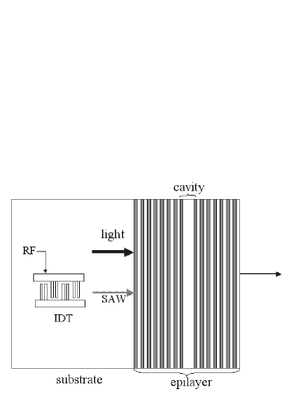
In photonic band gap (PBG) crystals, such as Bragg mirrors, a structural modulation is used to create a periodic change in the refractive index (and, consequently, in the dielectric function).5 This periodicity is comparable to the light wavelength. When a SAW with a wavelength much longer than the periodicity of the underlying PBG structure propagates across the structure, an additional time-dependent periodicity is superimposed on its dielectric function, as shown in Fig. 1. The solution to Maxwell’s equations has to include the effects of both the short- and the long-range periodicities. We have extended the mathematically rigorous transfer matrix (TM) method6-8 to the case where the unit cell in the direction of light propagation is a multiple of and the dielectric function varies with the SAW frequency . When light of frequency impinges on the PBG material, the transmission and reflection take place through channels of frequencies ( ) with .9 In the present calculations, we neglected the modes with . The size of the transmission and reflection matrices in the TM approach becomes, in this case, three times as large as that for a bare PBG structure (i.e., in the absence of a SAW). Care has been taken to remove numerical instability arising on account of the increase in the number of forward steps and in the matrix dimensions. The method has been found to be stable even for structures containing as much as 300 PBG unit cells in a SAW wavelength. The details of this calculational procedure will be published elsewhere.10
For ease of fabrication, we considered thin and planar structures, which can be grown with the current molecular-beam-epitaxy (MBE) technology. The composition and thickness of the layers as well as the total size of the layer stack were varied so as to enhance the interaction between light of wavelength of 940 nm and a SAW with m. The electric field concentration in the cavity is crucial for the enhancement of AO interaction. We found that the modulation is the largest when the cavity is placed close to, but not exactly at the center of the Bragg mirror structure. One possible structure is shown in Fig. 1. It is a 40-period asymmetric Bragg structure with a GaAs cavity near the center. The first 21 periods are alternating AlAs and GaAs layers with thicknesses of 76.9 nm and 65.5 nm, respectively, followed by the 142.4 nm-thick GaAs cavity and the second mirror, which has 18 periods with the same composition as the first Bragg mirror. This structure exhibits a forbidden gap of 117 nm (from 865 nm to 983 nm), as shown in the spectrum of its transmission coefficient in Fig. 2. The cavity states are located near 940 nm and have a full width at half maximum (FWHM) of about 0.5 nm. Although this design is for operation near 940 nm, the structure can be easily scaled for other operation frequencies.
In our calculations, we assumed that the SAW creates a sinusoidal modulation of the dielectric constant, as shown in Fig. 1, with a peak value for the relative modulation of the dielectric function /. From calculations of the SAW strain field, we determined that these dielectric modulation levels can be generated in GaAs/AlAs multilayers by conventional IDTs excited with a 500 MHz radio-frequency power of 20 mW. In Fig. 3, the calculated transmission coefficients through the central channel [, dots] and side channels [, squares] are compared with that obtained in the absence of a SAW [, open circles]. The inter- and the intra-channel scattering modes induced by the SAW have negligible intensities except at frequencies very close to the cavity states, where the AO interaction is strong. Although the transmission occurs through these three frequencies, the channels are separated only by a very small frequency . In experiments, the observed transmission coefficient will thus be the sum of the contributions from all three channels. Hence, the CR is defined as the ratio of to [+++-] and plotted as a dashed line in Fig. 3. A maximum CR of about 4 can be obtained. The dielectric modulation , which depends on the square root of the acoustic power,11-13 can be further increased by improving the IDT design. Previous calculations for a specific design13 within the GaAs/(Al,Ga)As system show that much larger ratios (of up to ) are possible. To investigate the operation of the switch under theses conditions, we show in Fig. 4 the calculated CRs for various values of /. CR increases almost quadratically with , reaching values as high as 300 for (corresponding to a relative refractive index change of 0.3%).
Layer size fluctuations inherently present in MBE growth may affect the properties of the Bragg mirrors and deteriorate the contrast ratio. This effect was modeled by assuming that the dielectric constants fluctuated randomly within 5% of their original values. We found that the highest CR decreases from 300 to 240. In addition, the central frequency may shift as the cavity thickness changes.
Although the structure proposed here can be grown by the MBE method, an unconventional placement of the IDT for SAW generation may be required. Since the dimensions of IDT for high frequency SAWs (1 GHz) can be significantly reduced below a mm, we suggest its placement on the side of the substrate, as shown in Fig. 5. In this configuration, both the SAW and the light beams travel along the direction perpendicular to the layer stack. Recent developments of electron-beam lithography and of imprint techniques14 for IDT fabrication may make such an arrangement possible. Another possibility is to generate the SAW on a highly piezoelectric material, such as LiNbO3 or ZnO, and then to couple it to the device structure on GaAs employing wafer bonding techniques.
While the cavity design leads to large CR values, it has a limited frequency tunability, because of the -function-like distribution of defect modes. A wider tunability range can be achieved if the SAW interacts with propagating light modes lying outside the forbidden gap of the Bragg mirror. The strength of the AO interaction, however, is considerably weaker for these extended modes.9,15 While operating near the zone edge might improve the AO coupling (because of the reduced light group velocity), longer SAW wavelengths and, consequently, longer interaction paths will be needed to ensure wave vector conservation. For shorter switches, such as the one based on the one-dimensional Bragg stack, it is clear that one has to work in a band with extremely small dispersion in order to achieve large light modulation efficiencies.
The major advantages of the optical switch proposed here are the potentially very high on/off CRs, sub-s switching times, and extremely small sizes. The frequency tunability (selection of ) is limited to a sub-nm range defined by the cavity states. If more cavity states are introduced to increase the energy width and the tunability range, the strength of the AO interaction will be reduced. The latter may be compensated by increasing the number of layer stacks. The growth of high-quality Bragg mirrors by MBE, however, is restricted to a maximum stack thickness of a few microns.
In conclusion, we have used an extended version of the TM approach to calculate the changes in the transmission spectra induced by SAWs in PBG crystals. We show that a large modulation of light can be achieved in a one-dimensional Bragg stack with a cavity. If the acoustic power can be increased to cause a 0.30% change in the refractive index near the cavity in the PBG structure, CRs of the order of a few hundred can be achieved through the AO effect.
The original TM code, written by A.J. Ward and J.B. Pendry, is from the Computer Physics Communication International Program Library. We thank Prof. J.B. Pendry for providing additional material to understand their computer code, Dr. A. Reynolds for a discussion on numerical stability, and Prof. H. Grahn for comments on the manuscript. Financial support (for S.K) from the Alexander von Humboldt Foundation, Germany, and from the Deutsche Forschungsgemeinschaft (for P.V.S., project No. SA598/3-1) is gratefully acknowledged.
REFERENCES
- [1] For example, N. Goto and Y. Miyazaki, Jpn. J. Appl. Phys., Part 1 37, 2947 (1998); and references cited therein.
- [2] P. Hess, Phys. Today, 55(3), 42 (2002).
- [3] C.W. Ruppel, R. Dill, A. Fischerauer, G. Fischerauer, W. Gawlik, J. Machui, F. Muller, L. Reindly, W. Ruile, G. Scholl, I. Schropp, and K.C. Wagner, IEEE Trans. Ultra. Ferro. and Freq. Control 40, 438 (1993).
- [4] S. Sanchez, C. De Matos, and M. Pugnet, Appl. Phys. Lett. 78, 3779 (2001).
- [5] J.D. Joannopoulos, R.D. Meade, and J.N. Winn, Photonic Crystals, (Princeton University Press, Princeton, 1995).
- [6] J.B. Pendry, J. Mod. Optics 41, 209 (1994).
- [7] J.B. Pendry, J. Phys. Cond. Matter 8, 1085 (1996).
- [8] A.J. Ward and J.B. Pendry, J. Mod. Optics 43, 773 (1996).
- [9] P.V. Santos, J. Appl. Phys. 89, 5060 (2001).
- [10] S. Krishnamurthy and P.V. Santos, (in preparation).
- [11] S. Datta, Surface Acoustic Waves, (Prentice-Hall, Englewood Cliffs, 1986).
- [12] S. Swierkowski, T. van Duzer, and C.W. Turner, IEEE Trans. Son. Ultrason. SU-20, 260 (1973).
- [13] F.C. Jain and K.K. Bhattacharjee, IEEE Photonics Tech. Lett. 1 307 (1989).
- [14] S.Y. Chou, P.R. Krauss, and P.J. Renstrom, Appl. Phys. Lett. 67, 3114 (1995).
- [15] W.F. Liu, P.St.J. Russell, and L. Dong, Opt. Lett. 22, 1515 (1997).