Etched distributed Bragg reflectors as three-dimensional photonic crystals: photonic bands and density of states
Abstract
The photonic band dispersion and density of states (DOS) are calculated for the three-dimensional (3D) hexagonal structure corresponding to a distributed Bragg reflector patterned with a 2D triangular lattice of circular holes. Results for the Si/SiO2 and GaAs/AlGaAs systems determine the optimal parameters for which a gap in the 2D plane occurs and overlaps the 1D gap of the multilayer. The DOS is considerably reduced in correspondence with the overlap of 2D and 1D gaps. Also, the local density of states (i.e., the DOS weighted with the squared electric field at a given point) has strong variations depending on the position. Both results imply substantial changes of spontaneous emission rates and patterns for a local emitter embedded in the structure and make this system attractive for the fabrication of a 3D photonic crystal with controlled radiative properties.
pacs:
42.70.Qs 41.20.JbI Introduction
Photonic crystals are being intensively studied with the goal of achieving a photonic band gap as well as control of light propagation and light-matter interaction at visible frequencies [1, 2, 3, 4]. A complete photonic gap in three dimensions (3D) has been demonstrated for the diamond lattice of dielectric spheres [5], the fcc lattice of air spheres (or “inverse opal”) [6, 7], the “yablonovite” [8], the “woodpile” [9], and other more complex 3D geometries [10, 11]. All these structures are difficult to fabricate at optical wavelengths: they often require the use of a bottom-up procedure, like e.g. in the case of inverse opals, where the template is first built by self-assembling of dielectric spheres in a solution and the voids are subsequently filled with a high refractive index material [12, 13, 14]. As an alternative, two-dimensional (2D) photonic crystals can be fabricated with a top-down approach based on lithography and etching. This procedure can be realized at sub-micrometric wavelength scales and allows for the controlled introduction of linear and point defects. A main problem however concerns the control of light propagation in the third (vertical) dimension: even in the case of a waveguide-embedded 2D photonic crystal, radiation losses due to out-of-plane diffraction in the vertical direction cannot be eliminated for photonic modes which lie above the light line [15, 16, 17].
In this work we explore theoretically another possibility for achieving control of light propagation in 3D, namely the use of distributed Bragg reflectors (DBRs) patterned with a 2D lattice in the layer planes. DBRs are dielectric multilayers which are periodic in one dimension (1D) [18, 19, 20], i.e., they represent 1D photonic crystals and have a band gap for propagation of light along the multilayer axis. By patterning and etching a DBR with a 2D lattice which possesses a photonic gap, a 3D photonic crystal with uniaxial (or biaxial) symmetry is obtained: if the 1D gap of the multilayer is made to coincide with the gap of the 2D structure, a common band gap for light propagating along the main crystal axes can be achieved. Although a complete photonic band gap in 3D is not expected (due to the angular dependence of the 1D and 2D gaps, or else to the anisotropy of the Brillouin zone), an appreciable control of the photonic density of states (DOS) and consequently of the spontaneous emission properties may be realized. In such a situation, the etched DBR represents a favorable system for the study of spontaneous emission control in 3D photonic systems, since local (and possibly active) defects can be introduced at the level of 1D epitaxial growth and of 2D lithographic design.
Here we focus on the simplest and most promising structure, namely a DBR patterned with a triangular lattice of holes: the planar structure is known to display a 2D photonic gap common to both polarizations of light, if the dielectric constant and air filling fractions are large enough [3, 21, 22, 23]. We calculate the 3D photonic band dispersion and the photonic DOS for parameters which are representative of the Si/SiO2 system (a typical high-index contrast DBR) and of the GaAs/AlxGa1-xAs system (with low index contrast). In particular, we determine the conditions for the 1D and 2D photonic gaps to overlap: since the 1D stop band of the DBR changes upon patterning, and the 2D lattice of holes is formed in a stratified medium, the overlap of the two band gaps represents a sort of selfconsistency problem. The density of states is found to be considerably reduced in correspondence with the overlapping 2D and 1D gaps. Also, the local density of states (which is the relevant quantity for spontaneous emission rates) shows strong variations and additional reductions as a function of position. These findings show that sizeable changes of spontaneous emission rates and patterns of a local emitter embedded in this anisotropic 3D structure should occur. The present results may also serve as guidelines for experimental groups which are attempting the fabrication of these structures.
II Theoretical method
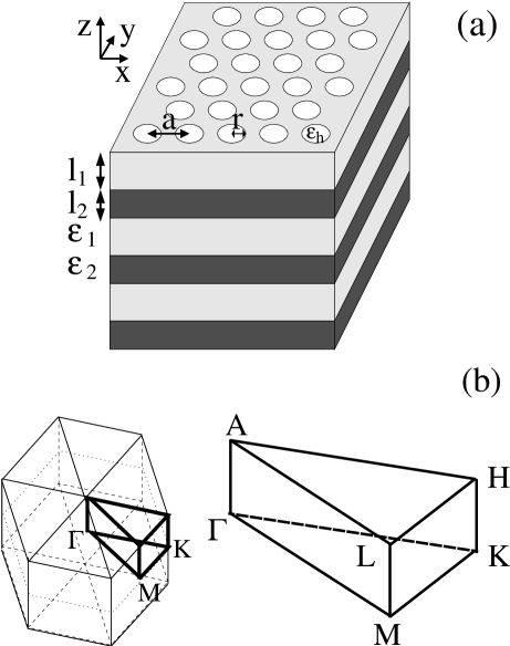
The geometry of the assumed structure is shown in Fig.1a. The axis is taken along the DBR growth direction. We denote by the thicknesses of the two DBR layers and by their respective dielectric constants. The 2D pattern in the plane is taken to be a triangular lattice of pitch , with a basis in the unit cell consisting of circular rods of radius and dielectric constant . In the present paper we consider only air holes (). The 3D Bravais lattice is simple hexagonal and the corresponding Brillouin zone with the main symmetry points is shown in Fig.1b. The DBR period is taken as a fixed length scale of the problem, in the sense that the photonic frequencies are given in dimensionless units : indeed, if such a structure is grown, a single epitaxial DBR can be patterned with various lateral periods at fixed . The 3D photonic lattice is fully determined by the ratios , , as well as by the dielectric constants .
In order to calculate the photonic band structure we start from the second-order vector equation for the magnetic field,
| (1) |
and use the well-known plane-wave expansion method. When reciprocal lattice vectors G are kept in the expansion, the equation is transformed into a matrix eigenvalue problem which contains the Fourier transform of the inverse dielectric constant . This is evaluated by the method of Ho, Chan and Soukoulis [5], which consists of calculating the Fourier transform of and inverting numerically the resulting matrix. This procedure yields a rapid numerical convergence when an energy cutoff is imposed for the number of reciprocal lattice vectors.
The density of states is defined as
| (2) |
where is the index of photonic bands and the sum over wavevectors extends over the first Brillouin zone. The local DOS is similarly defined as
| (3) |
In evaluating Eq. 3 the integral of the squared electric field is normalized to the unit cell volume, therefore DOS and local DOS have the same dimensions and can be directly compared. In order to calculate both quantities we adopt the linear tetrahedron method[24, 25, 26]. The DOS is already converged with a mesh of about 400 k-points in the irreducible wedge of the Brillouin zone (see Fig.1b). Calculating the local DOS requires a mesh which spans the whole Brillouin zone.
We now calculate the Fourier transform of the dielectric tensor, defined by
| (4) |
for the patterned DBR structure ( is the unit cell volume).

We write the 3D reciprocal lattice vectors as , where is the projection in the plane; similarly, . The unit cell volume is written as , where is the unit cell area for the 2D lattice. For a general patterning, the Fourier transform can be expressed in terms of a 2D structure factor
| (5) |
where the integral extends only over the unpatterned (or dielectric) region. Note that is the 2D dielectric filling fraction. For , the 3D Fourier transform is simply the average dielectric constant
| (6) |
For , it can be evaluated by subtracting the vanishing quantity from Eq. (4): the integrand now vanishes in the holes and the integral over the dielectric region yields the 2D structure factor (5), with the result
| (7) |
| (8) |
Note that the last expression is valid for any ( or ). The above equations (6)-(8) hold for a patterning with a general 2D lattice and holes of arbitrary shape: the 2D structure factor can be written as
| (9) |
For the present case of a triangular lattice of circular holes, the unit cell area is and the 2D structure factor becomes
| (10) |
| (11) |
where is the Bessel function of first order.
III Results
A Si/SiO2 system
We first consider the case of Si/SiO2 multilayers, modeled by the dielectric constants and . The Si/SiO2 system has the appealing features that the dielectric contrast is large, implying that a high rejection ratio in the stop band is obtained with a small number of periods, and that the etching of the two materials is a technologically well controlled process. Another high-index contrast system described by similar parameters is GaAs/Alox (oxidized AlAs) [27].
In Fig. 2 we show the photonic bands and density of states in the case of a Si layer width : this is close to the condition for the multilayer (i.e., when the two layer thicknesses are inversely proportional to their refractive indices) and it maximizes the 1D gap along the vertical direction. For the 2D lattice we choose and a hole radius : the latter value produces a full photonic band gap in the pure 2D case, when the refractive index contrast between dielectric and air is strong enough [3, 21, 22, 23]. Inspection of Fig. 2a shows that a 1D gap along the -A direction is indeed realized around , but also that no 2D gap occurs in the 2D projection of the Brillouin zone (-M-K- directions). The reason is that the average dielectric constant of the multilayer is too low to support a 2D band gap. In order to achieve a 2D photonic gap, the condition must be abandoned and multilayers with a higher Si fraction should be considered.
Concerning the photonic density of states, Fig. 2b shows that the DOS increases like at small frequencies (like for free photons) but pronounced structures occur when the photonic band dispersion deviates from linearity. In this and the following figures for the DOS, the dashed line represents the photon DOS in a homogeneous and isotropic medium with the same average dielectric constant of the etched DBR (Eq. 6), while the dotted line is the DOS of a homogeneous but uniaxial medium, whose dielectric tensor components are obtained from the in-plane and -A dispersions at small wavevector [28]. The dotted curve agrees with the numerically calculated DOS in the low-frequency (long-wavelength) limit; the dashed curve represents a reference DOS of an “average” medium, and is useful in order to tell whether the DOS of the etched DBR is reduced or increased with respect to that of the average medium.
In Fig. 3 we show the photonic bands and DOS of three Si/SiO2 multilayers with and : in all these cases the hole radius . A full 2D band gap in the -M-K- plane can be recognized in Fig. 3c (around ) and in Fig. 3e (around ), since the average dielectric constant of the multilayer is now close to the Si value. In Fig. 3a, the 2D gap should coincide with the second-order 1D gap at the point: however, the 2D gap is actually closed by a photonic mode which starts at the lower edge of the 1D gap at about . On increasing the ratio the 2D gap opens and decreases in energy, and for (Fig. 3e) it overlaps the first-order 1D gap at the A point.
In the case shown in Fig. 3e, it would seem that the 1D gap along -A is closed by a photonic mode which starts at the lower 2D gap edge around . However, since this mode is nondegenerate, it does not have the same symmetry of the electromagnetic field (which belongs to a twofold degenerate representation for any wavevector k along -A) and it cannot couple to an external beam incident along the -A direction: this mode is “symmetry uncoupled” [4, 29, 30, 31] and it cannot have any observable effect on the reflectance for a plane wave incident along the multilayer axis. Indeed, calculations of the optical properties [32] indicate that the etched DBR still behaves as a 1D reflector with a well-defined stop band along -A and with a reflectivity which tends to unity as the number of periods increases.
Concerning the photonic DOS, most features are similar to those of Fig. 2b already commented: however it is interesting to observe that a pronounced minimum occurs in correspondence with the 2D gap along -M-K- (e.g., around in Fig. 3f). In the frequency window of the 2D gap the DOS is reduced not only with respect to the “average” DOS (dashed line), but also in comparison with the DOS of the long wavelength limit (dotted line). The reduction of the DOS is particularly pronounced in the cases of Figs. 3 (b) and (f), when the 2D gap overlaps the 1D gap. Therefore, a reduction of spontaneous emission rates and a strong change of emission pattern is expected under these conditions: for the parameters of Fig. 3 (e,f), since spontaneous emission is suppressed in the plane and along the vertical direction (due again to symmetry mismatch between the emitted photon and the nondegenerate mode in the gap), the emission of a point-like dipole will be preferentially directed along the diagonals of the 3D structure.
In Fig. 4 we show the local density of states (LDOS) for the “optimal” parameters of Fig. 3(e,f), i.e., when the 2D and first-order 1D gap overlap. The LDOS is evaluated at three different positions along a line connecting two neighboring holes in the midplane of layer 1. The general behavior of the LDOS is similar that of the DOS, with a increase at small frequencies, a reduction in correspondence with the common 2D-1D gap and pronounced structures at higher frequencies. As discussed in connection with Eqs. 2,3, the DOS and LDOS are chosen to have the same units and can be directly compared, or in other words, the spatial average of the LDOS over all positions gives again the DOS. It can be seen that the LDOS is increased over the DOS of Fig. 3(f) for a position inside a hole (Fig. 4a or b), while it is considerably reduced at the center of the narrow dielectric region between two holes (Fig. 4c). The combined effects of a common 2D-1D gaps and of a change in position (i.e., of the electric field profile) results in a sizeable reduction of the LDOS: at and , the LDOS is equal to 4.4, compared to about 33 for the average medium. Therefore, the numerical results confirm that a strong reduction of spontaneous emission rates can be achieved for an emitter embedded in an etched DBR, when the parameters of the structure are properly chosen.


B GaAs/AlGaAs system
We now consider the case of GaAs/AlGaAs multilayers, modeled by the parameters and : the two values correspond to the dielectric constants of GaAs and AlGaAs, respectively, at 1 eV [33]. Since the two refractive indices are large and close to each other, the photonic energies in dimensionless units do not depend sensitively on the layer thicknesses and we choose them to be equal, : this is also close to the condition for the multilayer. In Fig. 5 we show the photonic bands and DOS with these parameters, assuming two different values and 1.8 and taking again a large hole radius . A 2D gap along -M-K- is formed (around in Fig. 5a, around in Fig. 5c) and in the case of it overlaps the small first-order 1D gap at the A point. Like in the case of Fig. 3e, the nondegenerate mode starting at the lower edge of the 2D gap is not coupled to a plane wave incident along the -A direction and it will not affect the normal-incidence reflectivity. Concerning the density of states, there is again an increase like at small frequencies followed by several structures. A reduction of the DOS occurs in correspondence with the 2D gap, with a minimum which is somewhat less pronounced than for the etched Si/SiO2 multilayers: this is due to the smaller refractive index contrast between GaAs and AlGaAs. Changes of spontaneous emission rates and patterns will also occur in the GaAs/AlGaAs system, but to a lesser extent than for a high index contrast structure.
IV Conclusions
Systematic calculations of photonic bands, total and local DOS have been undertaken for the hexagonal photonic structure corresponding to a distributed Bragg reflector patterned with a triangular lattice of holes. A few representative examples have been shown for the case of Si/SiO2 and GaAs/AlGaAs multilayers, focusing on the most favorable situations for achieving a full 2D photonic gap in the -M-K- plane. The parameters for which the 2D gap overlaps the 1D gap formed along the multilayer axis have been determined. A nondegenerate mode whose dispersion along -A overlaps the 1D gap is symmetry uncoupled from a plane wave propagating along -A and it will not affect the normal-incidence reflectivity.
The conditions for the overlap of a 2D and a 1D gap are rather restrictive and require a careful structure design: the average refractive index of the multilayer has to be large (thus the layer thicknesses must not obey the condition) and the air fraction of the 2D lattice must be such that a full 2D gap develops. The overlap of the 2D with the first-order 1D gap is found to occur around for the investigated structure, which is favourable in view of patterning the multilayers with lithography and etching techniques.
The photonic density of states has a pronounced minimum in correspondence with the common 2D-1D gap, particularly for the case of the Si/SiO2 system. The local DOS depends strongly on the position and is considerably reduced at the center of the dielectric veins between two holes. The combined effects of overlapping 2D-1D gaps and of the position dependent DOS will yield a strong reduction of spontaneous emission rates and considerable changes of emission patterns, with a redistribution of the emission mainly along the diagonal direction of the 3D structure.
Specific calculations of the optical properties of etched DBRs (reflectivity and spontaneous emission) are underway [32]. The anisotropic structure made of the etched DBR is concluded to be an interesting possibility for the realization of 3D photonic crystals where a controlled introduction of defects is possible and whose spontaneous emission properties can be tailored to a large extent.
Acknowledgements
The authors are grateful to Mario Agio for performing preliminary reflectivity calculations and for useful discussions. This work was supported in part by INFM PAIS 2001 project ”2DPHOCRY” and by MIUR through Cofin 2000 program.
REFERENCES
- [1] E. Yablonovitch, Phys. Rev. Lett. 58 (1987) 2059.
- [2] S. John, Phys. Rev. Lett. 58 (1987) 2486.
- [3] J.D. Joannopoulos, R.D. Meade, and J.N. Winn, Photonic Crystals - Molding the Flow of Light (Princeton University Press, 1995).
- [4] K. Sakoda, Optical Properties of Photonic Crystals (Springer, Berlin, 2001).
- [5] K.M. Ho, C.T. Chan, and C.M. Soukoulis, Phys. Rev. Lett. 65, (1990) 3152.
- [6] H.S. Sözüer, J.W. Haus, and N. Inguva, Phys. Rev. B 45 (1992) 13962.
- [7] K. Busch, and S. John, Phys. Rev. E 58 (1998) 3896.
- [8] E. Yablonovitch, T.J. Gmitter, and K.M. Leung, Phys. Rev. Lett. 67 (1991) 2295.
- [9] K.M. Ho, C.T. Chan, C.M. Soukoulis, R. Biswas, and M. Sigalas, Solid State Commun. 89 (1994) 413.
- [10] S. Fan, P.R. Villeneuve, R.D. Meade, and J.D. Joannopoulos, Appl. Phys. Lett. 65 (1994) 1466.
- [11] S.G. Johnson, and J.D. Joannopoulos, Appl. Phys. Lett. 77, (2000) 3490.
- [12] M.S. Thijssen, R. Sprik, J.E.G.J. Wijnhoven, M. Megens, T. Narayanan, A. Lagendijk, and W.L. Vos, Phys. Rev. Lett. 83 (1999) 2730.
- [13] A. Blanco, E. Chomski, S. Grabtchak, M. Ibisate, S. John, S.W. Leonard, C. Lopez, F. Meseguer, H. Miguez, J.P. Mondia, G.A. Ozin, O. Toader, and H.M. Van Driel, Nature 405 (2000) 437.
- [14] Y. A. Vlasov, X.-Z. Bo, J.C. Sturm, and D.J. Norris, Nature 414 (2001) 289.
- [15] P.L. Gourley, J.R. Wendt, G.A. Vawter, T.M. Brennan, and B.E. Hammons, Appl. Phys. Lett. 64 (1994) 687.
- [16] P.St.J. Russell, D.M. Atkin, T.A. Birks, and P.J. Roberts, in Microcavities and Photonic Bandgaps: Physics and Applications, edited by J. Rarity and C. Weisbuch (Kluwer, Dordrecht, 1996), p. 203.
- [17] H. Benisty, C. Weisbuch, D. Labilloy, M. Rattier, C.J.M. Smith, T.F. Krauss, R.M. De La Rue, R. Houdré, U. Oesterle, C. Jouanin, and D. Cassagne, J. Lightwave Technol. 17 (1999) 2063.
- [18] M. Born, and E. Wolf, Principles of Optics (Pergamon, Oxford, 1970).
- [19] A. Yariv, and P. Yeh, Optical Waves in Crystals (Wiley, New York, 1984).
- [20] H.A. McLeod, Thin-Film Optical Filters, 2nd ed. (Hilger, 1986).
- [21] P.R. Villeneuve, M. Piché, Phys. Rev. B 46 (1992) 4969.
- [22] R.D. Meade, K.D. Brommer, A.M. Rappe, and J.D. Joannopoulos, Appl. Phys. Lett. 61 (1992) 495.
- [23] R. Padjen, J.-M. Gérard, and J.-Y. Marzin, J. Modern Optics 41 (1994) 295.
- [24] O. Jepsen and O.K. Andersen, Solid State Commun. 9 (1971) 1763.
- [25] G. Lehmann and M. Taut, Phys. Status Solidi (b) 54 (1972) 469.
- [26] O. Jepsen and O.K. Andersen, Phys. Rev. B 29 (1984) 5965.
- [27] A. Fiore, V. Berger, E. Rosencher, P. Bravetti, and J. Nagle, Nature 391, 463 (1998).
- [28] The photonic DOS in a uniaxial medium is obtained by summing the DOS of ordinary and extraordinary modes: if is the free-space DOS and () is the refractive index for a polarization parallel (perpendicular) to the optic axis, the DOS is given by .
- [29] W.M. Robertson, G. Arjavalingam, R.D. Meade, K.D. Brommer, A.M. Rappe, and J.D. Joannopoulos, J. Opt. Soc. Am. B 10 (1994) 322.
- [30] K. Sakoda, Phys. Rev. B 52 (1995) 7982.
- [31] M. Galli, M. Agio, L.C. Andreani, M. Belotti, G. Guizzetti, F. Marabelli, M. Patrini, P. Bellutti, L. Dal Negro, Z. Gaburro, L. Pavesi, A. Lui, and P. Bellutti, Phys. Rev. B 65, 113111 (2002).
- [32] M. Agio, E. Pavarini, and L.C. Andreani, unpublished work.
- [33] Handbook of Optical Constants of Solids, edited by E.D. Palik (Academic Press, Orlando, 1985).
