S.J., V.M, and E.V. also, at Institute of Materials Science and Applied Research, Vilnius University, Saulėtekio 10, 2040 Vilnius, Lithuania
Microfabrication of Three-Dimensional Structures in Polymer and Glass by Femtosecond Pulses
Abstract
We report three-dimensional laser microfabrication, which enables microstructuring of materials on the scale of m. The two different types of microfabrication demonstrated and discussed in this work are based on holographic recording, and light-induced damage in transparent dielectric materials. Both techniques use nonlinear optical excitation of materials by ultrashort laser pulses (duration ps).
pacs:
direct laser writing, femtosecond microfabrication, photonic crystals, 3D optical memoryI Introduction
Technology used for the production of semiconductor microchips will soon enable industry-grade fabrication with smallest feature size of 100 nm. The new blue-laser DVD format, agreed upon in February 2002, will feature up to 27 GBytes of memory on one side of a single 12-cm disc, nearly six times the capacity of current 4.7 GBytes disks. However, these are the achievements of 2D microfabrication. Developing technologies of 3D fabrication which would enable to achieve minimum feature size of m is still a challenge, and attracts increasing interest. Tools for manipulation, handling, and fabrication on this scale are important for the future of microfabrication and microassembling techniques. The interest is also prompted by the biocompatibility issues, since the most crucial processes in living organisms occur on the length scale of m. The early works on 3D patterning were focused on the formation of ordered “optical matter” structures composed of microspheres Burns749 suspended in liquid solutions. The ordering was accomplished via the force exerted on the microspheres by periodical multi-beam light interference field Burns749 . Recently, we reported on fabrication of 3D structures in resist Kondo725 by using diffractive beam splitter and objective lens focusing, which were used to create a periodic pattern. 3D fabrication was achieved via one-photon absorption at 400 nm in the resist.
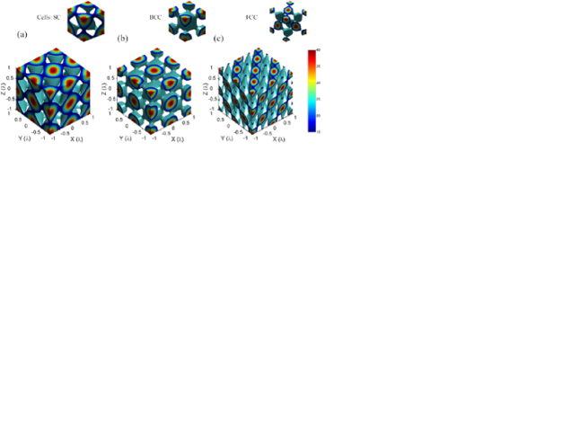
In this work we report a fabrication via two-photon absorption of 800 nm irradiation in resist. Such approach may be particularly useful for the fabrication of photonic crystals (PhC). It can be shown that any 3D Bravais lattice can be generated by the interference of four non-coplanar beams Cai . This is illustrated in Fig. 1 which shows calculated light intensity distributions having cubic lattice symmetry. In addition to such holographic recording, we also report 3D microstructuring by direct laser writing Miwa . This method is based on the light-induced damaging of materials. High irradiance laser pulses, tightly focused by high numerical aperture (NA) optics, induce permanent damage inside the bulk of optically transparent dielectrics; the size of the damaged region is usually smaller than 1 m owing to the tight focusing and nonlinear nature of the material excitation. The prove of a principle for Tbits/cm3 memory fabrication is demonstrated.
II Experimental
Holographic recording experiments were carried out using 150 fs duration pulses derived from a Ti:sapphire laser at the fundamental 800 nm wavelength. Multiple coherent beams were obtained from a single beam by using a diffractive beam splitter. For the direct laser writing, amplified pulses of fundamental wavelength from the same laser were used. Beam focusing was achieved by microscope objective lens. More details concerning the setup can be found elsewhere Kondo725 ; Miwa ; Watanabe . We have used commercial SU-8 photoresist (sensitive at 400 nm wavelength) for the holographic recording, and fused silica (transparent at 800 nm wavelength) for the direct laser writing experiments.
III Results and Discussion
III.1 Holographic recording
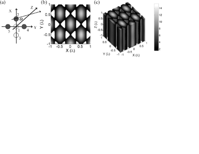
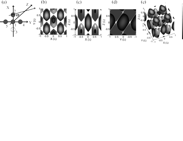
Prior to describing the experimental results, it is helpful to demonstrate theoretically the possibilities to obtain different 3D as well as 2D light interference patterns by using various numbers of plane waves with certain amplitude and phase. The simplest 2D structures can be fabricated by the three side beams (the central beams blocked) as shown in Fig. 2(a). The developed structure should be self-supporting, i.e., consist of well connected regions. An example of such structure is shown in Fig. 2(b), where the rod-like high intensity regions are joined into the self-supporting structure at the light intensity threshold of 1.5. For the PhC applications it may be important to control the volume fraction of the unexposed photoresist, later to be removed in the development process. This can be achieved by adjusting the exposure. When the central beam is turned on, 3D interference patterns may result as illustrated in Fig. 3).
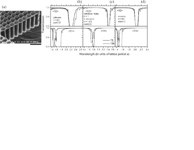
Image of the 2D pillar structure fabricated by the holographic technique is shown in Fig. 4(a). The recording wavelength used was 800 nm, at which two-photon absorption was required for the photomodification of the photoresist. The thickness of the photoresist film was m. High sample quality and periodicity is evident from the figure. In such structure spatial modulation of the dielectric constant may result in the formation of photonic bands, and therefore it is potentially applicable as a PhC. There is a growing interest in developing novel techniques of the PhC fabrication Mizeikis35 , and the holographic approach described above is potentially interesting in this respect. Simulated transmission spectra of the 2D PhC are shown in Fig. 4(b-d) for different directions of the light propagation, and different ratios between the column radius and the lattice period . Even if the refractive index contrast in the photoresist-air PhC structures is too low for the formation of photonic bandgaps, they can serve as templates for in-filling by other materials with higher refractive index.
III.2 Direct laser writing
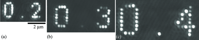
Figure 5 demonstrates optical readout of the 3D pattern recorded by femtosecond laser pulses of the fundamental wavelength in fused silica. Every bit was recorded in a single shot. The diffraction-limited spot radius (radius of I Airy disk) during the pattern recording was about 349 nm (Rayleigh criterion of resolution), whereas in the readout it was about nm for nm and . Since the recording involved nonlinear absorption processes, the recorded “bits” were considerably smaller than the focal spot (diameter) of 697 nm of the recording pulse. Due to this circumstance, 3D optical recording is possible with bit dimensions m, and astonishingly high information density of mTbits/cm3 can be expected (1 Tbit bits).
IV Conclusions
We have demonstrated holographic recording of 3D structures by interference patterns of multiple ultrashort laser pulses and direct laser writing by tightly focused laser pulses. Typical feature size achieved by these techniques can be easily decreased below the diffractive limit () owing to nonlinear mechanisms involved in the photmodification process. We have demonstrated direct laser writing in silica with information density of about 100 Tbits/cm3.
Acknowledgements.
This work was in part supported by the Satellite Venture Business Laboratory of the University of Tokushima.References
- (1) M. M. Burns, J.-M. Fournier, and J. A. Golovchenko, Science 249, 749 (1990).
- (2) T. Kondo, S. Matsuo, S. Juodkazis, and H. Misawa, Appl. Phys. Lett. 79(6), 725 (2001).
- (3) L. Z. Cai, X. L. Yang, and Y. R. Wang, Opt. Lett. (2002. in press).
- (4) M. Miwa, S. Juodkazis, T. Kawakami, S. Matsuo, and H. Misawa, Appl. Phys. A 73, 561 (2001).
- (5) M. Watanabe, H. Sun, S. Juodkazis, T. Takahashi, S. Matsuo, Y. Suzuki, J. Nishii, and H. Misawa, Jpn. J. Appl. Phys. 37(12B), L1527 (1998).
- (6) V. Mizeikis, S. Juodkazis, A. Marcinkevicius, S. Matsuo, and H. Misawa, J. Photochem. and Photobiol. C: Photochemistry Reviews 2, 35 (2001).