Giant Quantum Reflection of Neon Atoms from a Ridged Silicon Surface
Abstract
The specular reflectivity of slow, metastable neon atoms from a silicon surface was found to increase markedly when the flat surface was replaced by a grating structure with parallel narrow ridges. For a surface with ridges that have a sufficiently narrow top, the reflectivity was found to increase more than two orders of magnitude at the incident angle of 10 mRad from the surface. The slope of the reflectivity vs near zero was found to be nearly an order of magnitude smaller than that of a flat surface. A grating with 6.5 % efficiency for the first-order diffraction was fabricated by using the ridged surface structure.
Quantum reflection[1] of a particle is a reflection of wave nature that occurs as a result of impedance mismatch at a steep slope of interacting potential. The reflection occurs equally even when the particle is moving along the downhill slope of the potential. The reflectivity depends on the steepness of the spatial variation of the potential and approaches unity when the kinetic energy of the particle approaches zero. Quantum reflection was verified experimentally by the reflection of helium and hydrogen atoms on a liquid helium surface[2, 3, 4, 5] and, more recently, by the detection of specular reflection of metastable neon atoms from silicon and glass surfaces[1], which was caused by the attractive van der Waals potential near the surface. The quantum reflection due to the van der Waals potential occurs at a distance many times larger than the atomic separation of the solid, and the atomic scale irregularity of the solid surface is averaged out. The surface of the deflection is clearly defined within the distance of the de Broglie wavelength of an atom colliding on the surface. These features are in remarkable contrast to those of atom reflectors developed to date and closely resemble classical optical reflectors. Therefore, in principle, it should be possible to use quantum reflection as a tool to make simple, stable and nondispersive atom reflectors. However, the reflectivity from a flat solid surface decreases so rapidly with atomic velocity that its practical application is almost inconceivable. We discuss and experimentally demonstrate a new technique that improves the reflectivity many orders of magnitude by modifying the surface of the solid. By making the surface periodically ridged with a narrow flat top, we improved the reflectivity more than two orders of magnitude at an incident angle of 10 mRad. As an example of its application, we fabricated a reflective grating that had an efficiency of 6.5 % for the first-order diffracted atomic wave.
The atom will feel spatial variation of potential sufficiently steep when the change in the local wavevector within the distance becomes larger than , where is the wave vector of the atom at a large distance from the surface. Therefore,
For a power law potential with , takes the maximum value
| (1) |
at the distance
from the surface[6]. The atomic wave is partially reflected at the vicinity of , and the part of the wave that passes through the peak of is accelerated adiabatically and hits the repulsive wall of the surface. The increases indefinitely as the wave vector or the potential constant approaches zero, and the reflectivity is expected to approach unity if the normal incident velocity is sufficiently low or is sufficiently small. Since is approximately proportional to the density of the solid near the surface, the reflectivity should be improved by decreasing the effective density near the surface. Motivated by this consideration, we etched the silicon surface to form a grating structure with very narrow ridges so that the atom interacts with only a small fraction of the entire surface. We measured the reflectivity of an ultracold neon atomic beam in the metastable state as a function of incident angle.
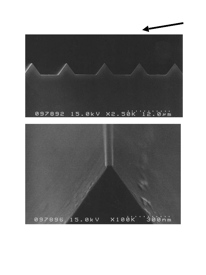
An example of the silicon surface used in the experiment is shown in Fig. 1. The grating structure was formed on the (0,0,1) surface that was flat within 20 nm, by the following procedure. A 100 nm-thick oxidized layer was formed on the (0,0,1) surface, then the surface was coated with a negative resist. The pattern of a periodic array of stripes that form the top of the ridges was written with an electron beam on the resist, and the oxidized layer was removed photo-lithographically with buffered HF excluding the top of the ridges. The direction of the ridge was aligned precisely parallel to the (1,1,0) direction. The silicon was then etched by tetramethylammonium (TMAH). The etchant preferentially etched the (0,0,1) surface and left facets on two sides of the oxidized stripe, forming a roof-shaped ridge. The etching process was stopped just before the bottom (0,0,1) facet disappeared, or the top of the ridge was eroded seriously. The height of the ridge was between 1.5 and 6 m. Finally, the oxidized layer on the ridge was removed with buffered HF. The flatness of the top of the ridge was believed not to be degraded by the etching process. The size of the plate was typically 10 mm by 90 mm. The ridge was formed parallel to the 10 mm side and was perpendicular to the atomic beam. We measured the reflectivity of several samples with a periodicity between 10 and 100 m and a width of the top of the ridge between 40 nm and 11m.
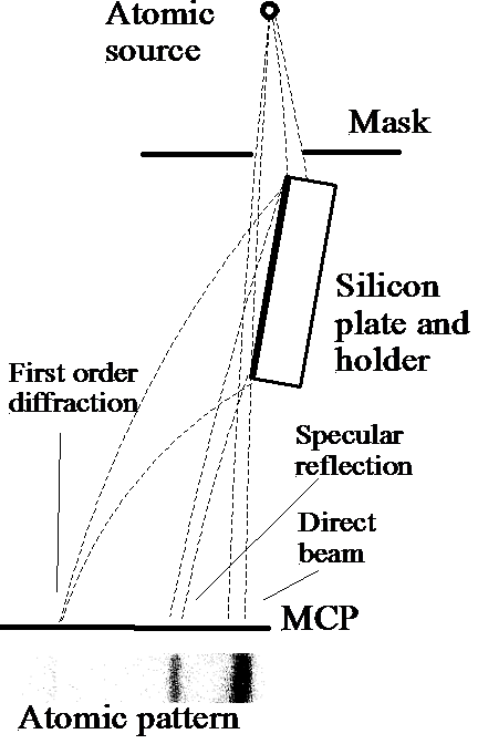
The experimental setup was described in our previous report[1]. Metastable neon atoms in the state were generated by optical pumping from atoms in the state trapped in a magneto-optical trap. The atoms were freed from the trap and fell nearly vertically pulled by gravity. A diaphragm with a square hole ( mm) was placed 33 cm below the atomic source. The silicon plate was placed 15 cm further below the diaphragm. Its surface was placed approximately parallel to a side of the square hole of the diaphragm. The longitudinal velocity of the atom at the surface was approximately 3 m/s, and its de Broglie wavelength was 7 nm. The entire vertical length of the silicon plate was illuminated by the atoms that passed through the square hole. A part of the atomic beam hit the plate, reflected and formed a line image on the microchannel plate detector (MCP) that was placed 112 cm below the atomic source. A part of the atomic beam missed the plate and hit the MCP directly. The intensity of the direct beam was used to calibrate the absolute reflectivity, while the angle of the reflection was calculated from the distance between the image of the reflected atoms and that of the direct beam. Figure 2 shows a cross-sectional view of the experimental setup and a typical pattern of atoms on the MCP. The pattern was obtained from the surface that had 1 m wide ridges and a periodicity of 100 m. The strong stripe in the middle is the image of the specularly reflected atoms. The weak line at the left is the first-order diffraction pattern produced by the 100 m periodic structure.
The reflectivity was measured at the normal incident velocity between 4 and 30 mm/s, which corresponded to the incident angle of the atomic beam measured from the silicon surface between 1.3 and 10 mRad. Figure 3 shows the reflectivity of four different samples as a function of normal incident velocity. For comparison, the curve for a flat surface taken from ref. 1 is shown by a solid line. The periodicity and the width of the four samples were m and m, m and m, m and nm, and m and nm, respectively.
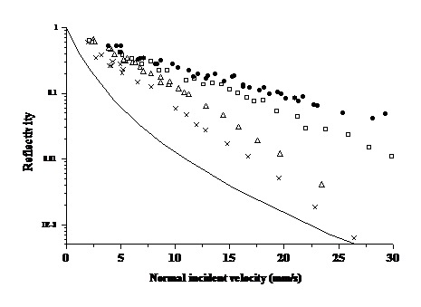
The one-dimensional wave equation with the potential is written in a dimensionless form if the distance is normalized by and the energy by . This means that, for the van der Waals potential , the reflectivity of a ridged surface is equal to the reflectivity of a flat surface at times smaller velocity, if the one-dimensional theory with replaced by is applicable. The actual improvement in the reflectivity is not that spectacular and shows that the two-dimensional wave equation must be integrated to obtain a quantitative result. However, the general trend in Fig. 3 agrees with this estimate. The reflectivity is larger for a smaller . The slope near for the samples with is approximately eight times smaller than that of the flat surface. As a result, at around the velocity of 30 mm/s corresponding to the incident angle mRad, the reflectivity was more than times larger than that of a flat surface . For the sample with a larger periodicity, the reflectivity decreased more rapidly than that of the flat surface at large . This result is easily understood based on geometrical consideration. When an atom passes near the top of the ridge, it must pass within distance in order to be deflected and to contribute to the specular reflection. An atom that passes at a larger distance can be deflected at the next ridge only when it does not hit the side of the ridge. By ignoring the numerical factor and putting in Eq. (1), is roughly given by , where is the de Broglie wavelength of the colliding atom. Therefore, when a substantial number of atoms are lost by hitting the side wall. For a periodicity of 100 m this angle is approximately 3 mRad.
Further improvement of the reflectivity at a larger angle will be possible if the width of the ridge and the periodicity are reduced. The reflecting distance decreases as the effective decreases and also as increases. The ultimate limit on the reflectivity is determined by the distance at which the colliding atom is influenced by interactions other than van der Waals potential. When the atom approaches too close to the surface, the interaction potential become flattened by the repulsive core potential and ceases to be sufficiently steep to cause reflection. A metastable atom can be inelastically scattered when it touches the electron on the solid surface. The distance to cause these phenomena is in the order of nm. Therefore, the ultimate normal incident velocity or the incident angle is determined by . For the metastable neon this gives the normal incident velocity of 50 cm/s. For a lighter atom such as helium the reflectivity should be high at any angles in principle if the atom is cooled below 100 K.
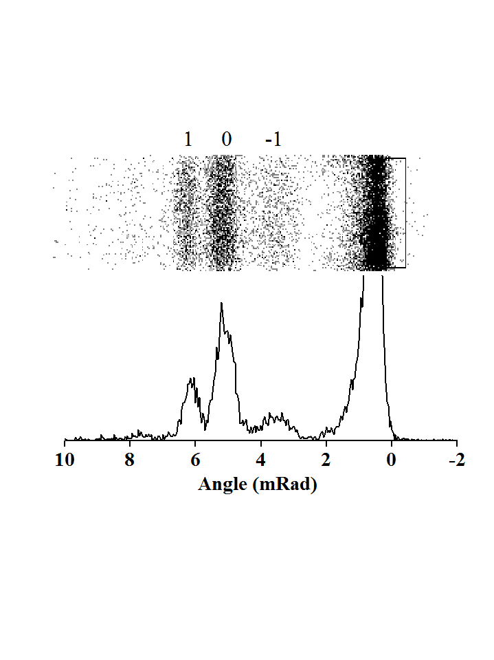
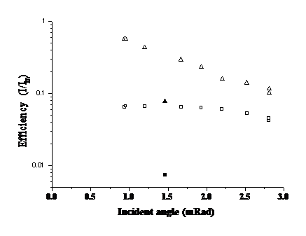
As an example of application to atom optical elements, we fabricated a reflective grating on a silicon surface with a ridged structure. Figure 4 shows the diffraction grating with a periodicity of 2 mm. The grating was composed of 1-mm-wide reflective stripes each of which was composed of ridges separated by 10 m. The top of the ridge was 100 nm wide. At a large diffraction angle, the intensity of the first-order diffraction relative to the specular reflection was approximately 0.4, which is in agreement with the intensity ratio of a transmission grating with a 50% opening. As the incident angle is reduced, the relative intensity of the first-order diffraction becomes weaker, and the efficiency becomes almost constant at a value of 6.5 %. This is due to the same physics that increases the reflectivity of a ridged surface. As the angle decreases, all atoms become deflected even when the spacing of two successive ridges is as large as 1 mm. Therefore, the 1-mm-wide flat stripe does not function as an absorbing surface, and the contrast of the amplitude grating is lost. A similar loss of contrast was observed on the phase grating of an evanescent wave[7].
In conclusion we have demonstrated that for light atoms the reflectivity of quantum reflection can be sufficiently increased for use as practical reflective atom optics elements, which enables us to design simple stable devices. The present result shows that the reflectivity changes markedly depending on the surface condition. Therefore, the quantum reflection is a valuable tool for studying the characteristics of solid surfaces.
Acknowledgments
This work was partly supported by the Grants in Aid for Scientific Research (11216202) from the Ministry of Education, Culture, Sports, Science and Technology. One of the author(FS) is grateful to C. I. Westbrook for valuable discussions.
References
- [1] F. Shimizu: Phys. Rev. Lett. 86 (2001) 987, and references therein.
- [2] V. U. Nayak, D. O. Edwards, and N. Masuhara: Phys. Rev. Lett. 50 (1983) 990.
- [3] J. J. Berkhout et al: Phys. Rev. Lett. 63 (1989) 1689.
- [4] J. M. Doyle et al: Phys. Rev. Lett. 67 (1991) 603.
- [5] I. A. Yu et al: Phys. Rev. Lett. 71 (1993) 1589.
- [6] For more accurate discusions, see, for example, C. Carraro and M. W. Cole: Prog. Surf. Sci. 57 (1998) 61.
- [7] L. Cognet et al: Phys.Rev. Lett. 81 (1998) 5044.