[
Mini-stop bands in single-defect photonic crystal waveguides
Abstract
We numerically study single-defect photonic crystal waveguides obtained from a triangular lattice of air holes in a dielectric background. It is found that, for medium-high air filling ratios, the transmission has very small values in narrow frequency regions lying inside the photonic band gap - the so-called mini-stop bands. Two types of mini-stop bands are shown to exist; one of which is due to the multimode nature of the waveguide. Their dependence on the length of the waveguide and on the air filling ratio is presented.
pacs:
42.70.Qs,42.82.Et]
Photonic band gap (PBG) materials, also known as photonic crystals (PCs), have been extensively studied recently because of their ability to control the propagation of light[1, 2, 3]. A very promising application of PBGs is for improving the performance of waveguides[4, 5, 6, 7, 8, 9, 10, 11]. A photonic crystal waveguide is basically a PC with a linear defect, which allows the propagation of light in a specific direction. PC waveguides provide a superior guiding mechanism with respect to dielectric or metallic waveguides since they are ideally loss-less, because of the PBG properties. Guiding the light without losses, and even through sharp corners using two-dimensional (2D) PCs was studied theoretically[4] and experimentally, both in microwaves[5] and in optical[6, 7, 8, 9] regimes. To eliminate out-of-plane losses in 2D PC structures, one has to use a index-guiding mechanism in the vertical direction[10, 11, 12, 13].
Detailed numerical studies of straight PC waveguides of different widths, in a high dielectric background[14, 15] and in air[16], have revealed that a complete frequency gap, called mini-stop band (MSB) or mode-gap, exists for the guided modes of the waveguide. The term MSB[15] refers to an anti-crossing mechanism between guided modes of different order; whereas the term mode-gap[16] is used for the band splitting of the folded guided mode at the edge of the one-dimensional (1D) Brillouin zone. Indeed, a straight PC waveguide is actually a system with a discrete periodicity along the waveguide’s axis, in which the 1D periodic potential given by the PC may produce mode couplings whenever the Bragg condition is fulfilled. Existence of MSBs has also been experimentally demonstrated by Olvier et al.[15] for waveguides in GaAs based PC heterostructures. In all of the previous studies no MSBs were observed for the 2D PC waveguide, which has one row of cylinders missing (single-defect waveguide). We adopt the term MSB to refer both the anti-crossing and the band splitting of a folded mode.
The purpose of this work is to investigate the single-defect PC waveguide
for a triangular lattice of air holes in a dielectric background,
showing the occurrence of MSBs.
Their dependence on the length of the waveguide and on the air
filling ratio will be presented and connections with the Fabry-Perot
modes of the 1D cavity made of the linear defect
will be discussed. The dielectric
constant of the background is chosen to be 11.56, which
corresponds to GaAs at the wavelength of .
The 2D PC has a gap for the TE mode, whose width depends[1]
on the air filling ratio . TE is the mode which has the magnetic field
parallel to the axes of the air cylinders.
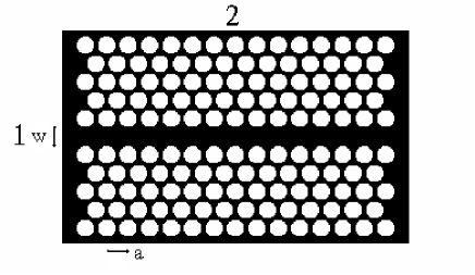
One can easily create a waveguide by removing a row of air holes.
This structure is shown in Fig. 1, where is the lattice constant
and is the width of the waveguide.
The waveguide has variable length in the dense direction
( direction). The field confinement in the perpendicular
direction () is provided by 5 PC rows arranged
at both sides of the waveguide. Numerical results have been obtained with
a 2D finite-difference time-domain (FDTD) method[17],
implemented with Liao absorbing boundary conditions[18].
The numbers 1 and 2 in Fig. 1 represent the positions of the FDTD
source: position 1(2) means transmission along the direction.
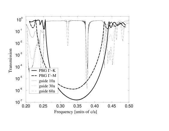
In Fig. 2, we present the results for the
case of for both the perfect periodic case, as well as
the waveguide case (source in position 1). Inside
the gap of the periodic photonic crystal, the transmission coefficient
of the waveguide is above 80%[19], for almost all frequencies.
Notice that there are two frequencies
(units of ), where the transmission is low.
We attribute these gaps in the
transmission to MSBs, i.e. gaps in the dispersion relation.
Notice also, that, as we increase the length of the waveguide, both
the drops of the MSBs get larger, as expected. On the other hand,
for frequencies corresponding to a guided mode, the transmission is
independent of the length of the waveguide[19].
Since the size of the PBG and the width are related to ,
we have addressed the spectral behaviour of the transmission for
different values of .
In Fig. 3, we plot the width of the gap for the periodic PC, as well as the frequencies and of the two MSBs versus . From Fig. 3, one sees that for small , there is no MSB inside the gap of the periodic system. This is the reason that no MSBs were seen in previous studies[14, 15, 16] of single-defect PC waveguides. Notice that for large , more than two MSBs are seen. These additional MSBs present a dispersion with similar to the MSBs found for .
To understand the character of the MSBs, we plot in Fig. 4 the intensity of the electric field at the mid-gap frequency for the low- and high-frequency MSB for the case . In Fig. 4(a), the profile extends all over the waveguide and it is a “Bloch-like” wave, similar to the pattern of the fundamental guided mode. However, it slowly decays as the field propagates through the waveguide. Notice that the PC waveguide is a 1D periodic system with a unit cell of length , whose reduced Brillouin zone is . The modulated dielectric constant of the PC, in addition to the PBG confinement, entails also a periodic potential, which shall couple guided modes satisfying the Bragg condition.

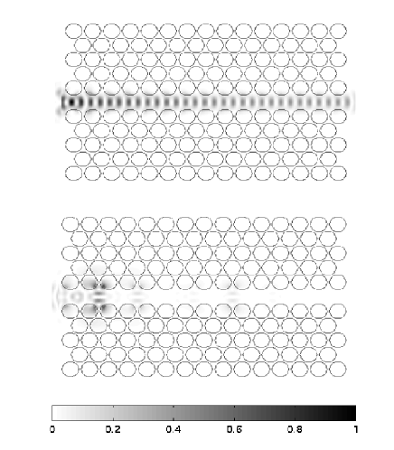
Returning to Fig. 4(a), if one counts the nodes in the field pattern along , it is found that the wavelength is roughly equal to ; i.e. the unfolded wave-vector is , corresponding to in the first Brillouin zone. At , the periodic potential couples the two counterpropagating fundamental modes (), which would be otherwise degenerate. Therefore, with Fig. 2 and Fig. 4(a) in mind, we recognize this MSB as the gap in the folded fundamental guided mode for .

The profile shown in Fig. 4(b) is completely different than that shown in Fig. 4(a). The electric field is now strongly localized and has nodes along . Above the frequency of the MSB, the field pattern returns to be that of the fundamental guided mode. This suggests the existence of another gap in the dispersion relation of the fundamental mode. According to Fig. 4, the origin of the high-frequency MSB cannot have the same nature of the low-frequency MSB, otherwise the field patterns would be similar. We suspect that this MSB is due to a coupling (anti-crossing) between the fundamental mode and a higher mode. To check this idea, we have to find evidence of at least one higher guided mode at frequencies inside the PBG. Since there is a correspondence between the cut-off frequency of a guided mode and the resonant frequency of a Fabry-Perot mode[15, 20], the search for cavity modes indirectly proves the existence of guided modes.
The PC waveguide of Fig. 1 can be seen as a 1D cavity when the source is in position 2, see Fig. 1, and the progagation is along the direction. We have calculated the transmission coefficient for such 1D cavity and show the results in Fig. 5. As one can clearly see, there are two peaks in the transmission, which correspond to two cavity modes. The high frequency peak is very close to the MSB; the low-frequency peak does not align with any MSB. Looking at the field patterns of the cavity modes, we indeed find that the high-frequency peak has the same symmetry and the same number of nodes as the field for the MSB at . We infer that the MSB stems from the anti-crossing between the fundamental mode and the higher mode with a cut-off frequency given by the corresponding cavity mode. The low-frequency cavity mode is odd with respect to the axis; for the PC waveguide of Fig. 1 the odd modes cannot couple to even modes[14, 15]. This is the reason for the absence of a MSB close to the “odd” resonant frequency.
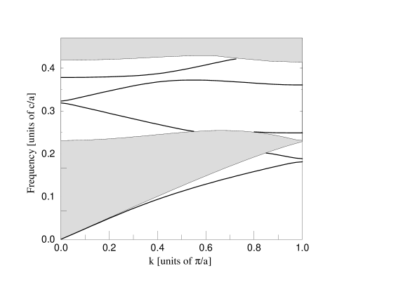
To give more insight of the MSBs, we have also calculated the band structure
for the even TE modes of the waveguide shown in Fig. 1, with .
The results are plotted in Fig. 6. The horizontal axis is the wavector in
the direction of the guide, and the band structure is presented in the
reduced Brillouin zone scheme. The gray areas are the projections of
every mode in the band structure of the perfect crystal.
We focus only on the guided modes ranging in the PBG
frequencies. The low-frequency MSB
is coming from the folding of the fundamental mode at
=0, as deducted from the previous field analysis.
The high frequency MSB is coming from the anti-crossing between the
fundamental and the higher order mode.
This guided mode has a cut-off frequency and
a small negative dispersion.
The weak depedence of the low-frequency MSB on f, shown in Fig. 3,
relies on the fact that the fundamental mode is almost concentrated
in the dielectric channel. Therefore, its dispersion relation feels
the filling factor only through the width ; likewise
is for the position of the low-frequency MSB. On the other hand, the higher
modes are more extended in the PC region and their dispersion relation
will be more sensitive to the filling ratio. The high-frequency MSB,
which is an anti-crossing between two dispersion relations
(fundamental mode-higher mode) will change its position according to the
higher mode, which encounters the fundamental mode at higher frequencies
as the filling ratio is increased. In other words, the fundamental
mode is guided by the high index path, as for a dielectric waveguide,
and the PBG is not important. On the contrary, the higher guided mode
does exist because the field confinement is provided by the PBG.
We have undertaken dispersion relation
calculations for values of where more than two MSBs exist.
The higher-frequency MSB-1, see Fig. 3, is a band splitting of the
fundamental mode at , whereas the higher-frequency MSB-2
is not a neat MSB, but a more complicated coupling among the
guided modes and the photonic bands at the bulk gap’s edge.
Moreover, from transmission studies, we have noticed a similar
behaviour for the first and third MSBs, and for the second and fourth
MSBs respectively.
We have observed that the transmission through single-defect PC waveguides has very small values in narrow frequency regions, the so-called MSBs. There are two types of MSBs and they are due to the 1D periodic potential of the PC along the waveguide. One MSB comes from the splitting of the folded fundamental guided mode at the zone edge of the reduced Brillouin zone; the other one comes from the anti-crossing between the fundamental mode and the higher order mode. The fundamental mode is sustained by a index guiding mechanism, whereas the higher modes are distinctive of PC waveguides and they are confined by the PBG. This difference is found in the dependence of the MSBs’ position on the filling ratio as well as in the dispersion relation.
We would like to thank S. Foteinopoulou, L.C. Andreani and S.G. Johnson for helpful discussions. This work was supported by the IST project PCIC and NSF Grant No. INT-0001236. Ames Laboratory is operated for the U.S. Department of Energy by Iowa State University under Contract No. W-7405-Eng-82.
REFERENCES
- [1] J.D. Joannopoulos, R.D. Meade, and J.N. Winn, Photonic Crystals, (Princeton University Press, New York, 1995).
- [2] see for example, “Photonic Band Gap Materials”, ed. by C. M. Soukoulis NATO ASI Series Vol. 315 (Kluwer, Dordrecht, 1996).
- [3] J.D. Joannopoulos, P.R. Villeneuve, and S. Fan Nature, 386, 143 (1997).
- [4] A. Mekis, et al., Phys. Rev. Lett. 77, 3787 (1996).
- [5] S.-Y. Lin, et al., Science 282, 274 (1998).
- [6] T. Baba, N. Fukaya, and Y. Yonekuva, Electron. Lett. 35, 654 (1999).
- [7] M. Tokushima, H. Kosaka, A. Tomika, and H. Yamada, Appl. Phys. Lett. 76, 952 (2000).
- [8] M. Loncar, et al., Appl. Phys. Lett. 77, 1937 (2000).
- [9] C.J.M. Smith, et al., Appl. Phys. Lett. 77, 2813 (2000).
- [10] D. Labilloy, et al., Phys. Rev. Lett. 79, 4147 (1997); H. Benisty, et al., J. Lightwave Technol. 17, 2063 (1999).
- [11] E. Chow, et al., Nature, 407, 983 (2000).
- [12] A. Chutinan, and S. Noda, Phys. Rev. B 62, 4488 (2000).
- [13] S.G. Johnson, et al., Phys. Rev. B 60, 5751 (1999); ibid. 62, 8212 (2000).
- [14] H. Benisty, J. Appl. Phys. 79, 7483 (1996); C.J.M. Smith, et al., Appl. Phys. Lett. 77, 2813 (2000).
- [15] S. Olivier, et al., Phys. Rev. B, 63, 113311 (2001); Opt. Q. Electr. to be published (2001); and private communication.
- [16] A. Mekis, S. Fan, and J.D. Joannopoulos, Phys. Rev. B 58, 4809 (1998).
- [17] A. Tavlove, Computational Electrodynamics - The Finite-Difference Time-Domain Method (Artech House, Norwood, MA, 1995).
- [18] Z.P. Liao, H.L. Wong, B.P. Yang, and Y.F. Yuan, Scientia Sinica (series A) Vol. XXVII, 1063-1076 (1984).
- [19] Because of the coupling efficiency of the incident and outgoing waves with the guided mode, the peak transmission could result less than one. To improve the coupling, we use a source with a spatial profile close to that of the fundamental guided mode of the PC waveguide. The fact that the transmission is independent of the length of the waveguide confirms that “losses” are not intrinsic and have to be referred to the non-optimal coupling efficiency.
- [20] K.L. Kliewer, and R. Fuchs Phys. Rev. 150, 573 (1966); and references therein.