SLAC-PUB-8846
May 2001
Impedance Analysis of Bunch Length Measurements at the ATF Damping Ring***Work supported by Department of Energy contract DE–AC03–76SF00515, and by the Chinese National Foundation of Natural Sciences, contract 19975056-A050501.
K.L.F. Bane,
T. Naito333High Energy Accelerator Research Organization (KEK),
1-1 Oho, Tsukuba, Ibaraki, Japan.
, T. Okugi33footnotemark: 3, Q. Qin444Institute of High
Energy Physics (IHEP), Beijing, People’s Republic of China., and J. Urakawa33footnotemark: 3
Stanford Linear Accelerator Center, Stanford University,
Stanford, CA 94309 USA.
Abstract
We present energy spread and bunch length measurements at the Accelerator Test Facility (ATF) at KEK, as functions of current, for different ring rf voltages, and with the beam both on and off the coupling resonance. We fit the on-coupling bunch shapes to those of an impedance model consisting of a resistor and an inductor connected in series. We find that the fits are reasonably good, but that the resulting impedance is unexpectedly large.
Presented at the 10th International Symposium on Applied Electromagnetics and Mechanics (ISEM2001)
Toshi Center Hotel, Tokyo, Japan
May 13-16, 2001
1 Introduction
In future e+e- linear colliders, such as the JLC/NLC, damping rings are needed to generate beams of intense bunches with very low emittances. A prototype for such damping rings is the Accelerator Test Facility (ATF)[1] at KEK. One important consideration for such rings is that the (broad-band) longitudinal impedance be kept sufficiently small, to avoid (longitudinal) emittance growth caused by potential well distortion and/or the microwave instability. Measurements of energy spread and bunch length as functions of current are a way of verifying the size of the impedance and its effects. The ATF, as it is now—running below design energy and with the wigglers turned off—is strongly affected by intra-beam scattering (IBS), an effect that modifies all dimensions of the beam. To study the impedance effects alone, however, the machine can be run on a (difference) coupling resonance, where the vertical beam size grows and the IBS forces become weak.
Calculations of the impedance of the ATF ring vacuum chamber yield a total inductive component (at the typical bunch lengths) of nH[2]; the dominant resistive component, the rf cavities, are expected to contribute . To obtain the impedance from bunch shape measurements, if the data is noisy (as it will be in our case), we need to fit to a relatively simple model of impedance. A pure resistor[3], a pure inductor[4], and a broad-band resonator[5] are all impedance models that have been used to characterize the impedance of storage rings. A simple model that can account for both potential well bunch lengthening and parasitic mode losses is a resistor and an inductor connected in series. This model was used to analyze bunch length measurements at CESR, where it appeared to fit the data well[6]. In this report we present bunch length measurements at the ATF, we use this model to estimate the real and imaginary parts of the ATF impedance, and then we compare our results with the earlier estimates.
2 Measurements
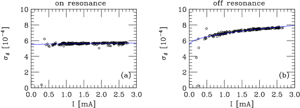
To obtain the beam energy spread in the ATF damping ring, the beam width is measured after extraction on a thin screen in a region of high dispersion. In Fig. 1 we plot the measured rms energy spread vs. current for peak rf voltage kV, for the case of the beam on resonance (a), and off (b). We note that, by mA, on the coupling resonance the energy spread growth is still very small (3%), whereas off resonance it is not (36%). Note also that Fig. 1a implies that the threshold to the microwave instability—whose signature would be a kink in the data—must be beyond mA.
The bunch length in the ATF ring was measured using a Hamamatsu C5680 streak camera. The data taking process consists of storing a high current beam, and then measuring the longitudinal bunch profile 50-70 times at fixed time intervals, while the current naturally decreased. The profiles were stored to disk, along with their DCCT current monitor readings. The measurements were repeated for , 200, 250, 300 kV, and for the beam both on and off the coupling resonance. Each trace was fit to an asymmetric Gaussian composed of two half-Gaussians with lengths , where is the rms bunch length and the asymmetry parameter. The parameters () gives us information about the imaginary (real) part of the impedance. Note that for the asymmetric Gaussian , where is the skew moment of the distribution. Note also that we expect the bunch to lean forward, which, in our convention, will mean . Instead of the 3rd moment we would prefer to use the 1st moment of the bunch distribution to probe the real part of the impedance; the streak camera trigger, however, is not accurate enough to resolve the kind of centroid shifts needed (on the order of picoseconds).
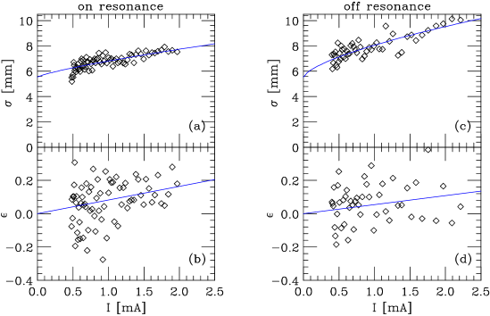
Results for kV are shown in Fig. 2. We note that increases with current, even on resonance (at 2mA the growth is 40%), implying that there is significant potential well distortion in the ATF. Off-resonance, however, the growth is much larger (at 2mA, 72%), due to IBS. As for the asymmetry parameter, we see much scatter in the data. We fit the results with a straight line through the origin (see Fig. 2b,d). On-resonance we find that mA, and it decreases slightly with . Note that for all eight sets of measurements (four voltages, both on and off the coupling resonance) the slopes are positive, as we expect from physical considerations. Thus, despite the large scatter in the data, there appears to be physical information in the fitted (or equivalently, the skew moment of the distribution) that we can draw out through statistics. Finally, note that more details of the bunch length measurements can be found in Ref.[7].
3 Haïssinski Solution for an Impedance
To obtain the steady-state bunch distribution for a series impedance we begin with the Haïssinski equation[8]:
| (1) |
where the induced voltage is given by
| (2) |
with the bunch position distribution, longitudinal position ( is toward the front of the bunch), the slope of the rf voltage at the synchronous point, the nominal (zero current) bunch length, and the (point charge) wakefield. Note that . Eq. 1 can be written as a first order, non-linear differential equation
| (3) |
For the special case of a resistive plus inductive impedance in series, with resistance and inductance ,
| (4) |
For this case, Eq. 3 can be written in normalized units as
| (5) |
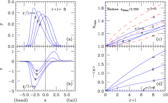
where , . The normalized induced voltage . Note that there are two free parameters in our equation: the (normalized) resistance times current, , and the (normalized) inductance times current, . To solve Eq. 5, we begin at a position far in front of the bunch, choose (a small number), numerically solve the differential equation, and compute the total integral of . We then iterate this process, adjusting until the integral equals 1.
Numerical results are shown in Fig. 3. In (a,b) we show representative bunch shapes and induced voltages for the example ; in (c,d) we give the first and second moments of the bunch shape, and also the full-width-at-half-maximum , as functions of .
4 Fitting to Bunch Length Measurements
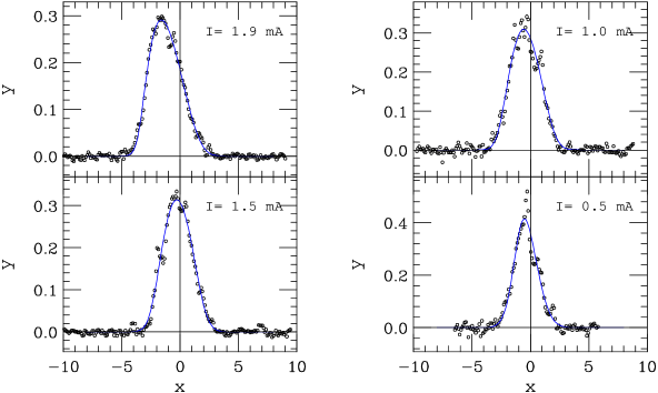
We fit the on-coupling bunch length measurements to , where is the Haïssinski solution to the impedance. The fitting parameters are , , , , , and , a centroid shifting parameter. We use the Method of Maximum Likelihood to do the error analysis, a method that assumes all errors are purely random and normally distributed[9]. Fig. 4 shows four sample fits (here is in the unshifted Haïssinski frame). We see some scatter in the data, though the fits are reasonably good.
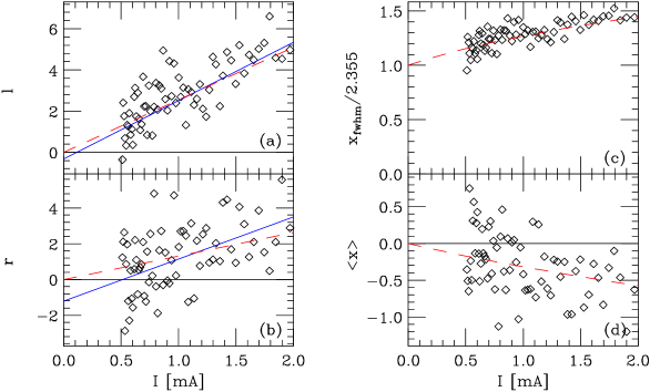
In Fig. 5 we summarize the fits for kV. Shown are the fitting parameters (a) and (b); the full-width (c) and centroid position (d) of the fitted distributions. In (a) and (b) the solid lines are least squares fits to the results, the dashed lines are least squares fits through the origin. We see that the least squares fit for naturally passes very close to the origin; the fit for , however, does not pass so close, indicating that the resistive part of the model does not fit as well. (This observation is also true for the cases of the other rf voltages.) Nevertheless, as our solution we take the least squares fit through the origin for both parameters (the dashes). The resulting full-width and centroid shift are given by the dashes in (c,d). We should note also that the fitted values of , a parameter that should be proportional to the bunch charge, correlated very well with the actual DCCT current readings.
In Table 1 we give a summary of the fitting results for the four different voltages. From the scatter in the entries the overall results are estimated to be: k and nH. When the measurements were repeated six months later, and a slightly different analysis was applied, the results were: k and nH.
| (kV) | (k) | (nH) |
|---|---|---|
| 150 | 1.3.05 | 54.7 |
| 200 | 1.7.05 | 50.6 |
| 250 | 1.1.04 | 39.4 |
| 300 | 0.8.04 | 35.4 |
5 Discussion
From Table 1 we note that the scatter in the results, for both and , is much larger than the estimated errors, implying that there are significant systematic errors or problems with the model. Systematic errors might include problems with the streak camera, such as residual space charge or aberrations in the optics. Error in the rf voltage, and consequently in the parameter , can also contribute to a systematic error in the results, though we don’t think that this a significant effect. To improve the fit to the data (remember: the least squares fit to the fitted deviated from the origin) a different impedance model, such as a broad-band resonator, can also be tried. Nevertheless, the fits to our model were fairly good and the results are reasonably consistent, at least to (20-30)%.
The impedance values implied by our analysis are much larger than expected: is about a factor of 3 larger than earlier calculations, and is about a factor of 10 larger, a result that is especially puzzling. To see whether there actually is such a large, resistive impedance in the ATF, it is planned, in the near future, to directly measure the beam synchronous phase shift with current using a synchroscan streak camera, one whose timing is accurately tied to the rf system timing. With such hardware, we believe that the expected 2-3 degree phase shift (at 714 MHz) in going from high to low current should be relatively easy to detect.
References
- [1] F. Hinode, editor, KEK Internal 95-4 (1995).
- [2] E.S. Kim, Proc. of the 1st Asian Particle Acc. Conf. (APAC98), Tsukuba, Japan, 1998, 489.
- [3] See, e.g., R. Holtzapple, SLAC-R-0487, PhD Thesis, June 1996.
- [4] See, e.g., K. Bane, SLAC-PUB-5177, February 1990.
- [5] See, e.g., A. Hoffman, et al, IEEE Trans. Nucl. Sci., NS-26, No. 3, 3514 (1979).
- [6] R. Holtzapple, et al, Phys. Rev. ST Accel. Beams, 3:034401, 2000.
- [7] K. Bane, et al, KEK-ATF Report 00-05, May 2000; T. Naito, et al, KEK-ATF Report 01-01, January 2001.
- [8] J. Haïssinski, Il Nuovo Cimento, 18B, No. 1, 72 (1973).
- [9] See, e.g., P. Bevington and D. Robinson, Data Reduction and Error Analysis for the Physical Sciences, 2nd Ed., (McGraw-Hill, Inc.) 1992.