A Measurement of Lorentz Angle of Radiation-Hard Pixel Sensors
Abstract
Silicon pixel detectors developed to meet LHC requirements were tested in a beam at CERN in the framework of the ATLAS collaboration. The experimental behaviour of irradiated and not-irradiated sensors in a magnetic field is discussed. The measurement of the Lorentz angle for these sensors at different operating conditions is presented. A simple model of the charge drift in silicon before and after irradiation is presented. The good agreement between the model predictions and the experimental results is shown.
1 Introduction
In the presence of an electric field and a magnetic field mutually orthogonal the charge carriers move along a direction that forms an angle ( Lorentz angle ) with the electric field. This angle affects the area of collection of the charge carriers.
Resolution and efficiency of the detector depend on the track incidence angle and on the charge drift angle: the determination of this angle is therefore very important to define the mechanical design and optimize detector performance.
The silicon pixel detector of the ATLAS experiment will be exposed at intense fluxes of radiation during its lifetime; as a result the properties and the conditions of operation of the sensors will change. Several single chip assemblies were characterised extensively in test beam experiments performed at the CERN SPS accelerator with a pion beam of 180 GeV/c momentum [2].
A beam telescope consisting of 4 pairs of silicon microstrips detectors (each pair consisting of two planes of detectors with orthogonal strips) was used to measure the transverse position of the incident beam particles. The pixel assemblies and the silicon strip telescope were positioned inside a magnet for the measurement of the Lorentz angle.
1.1 ATLAS Pixel Sensors
A detailed description of the ATLAS pixel sensors can be found in [1, 3], so only a brief description is given here. The sensor is a matrix of 18 160 n+ implants on a high resistivity n-bulk substrate. This choice allows for operation in partially depleted mode after bulk inversion induced by radiation damage. The isolation between n+ pixels is obtained using the newly developed p-spray technique [4]. The dimensions of pixel cell are 50 400 . The pulse height measurement is performed by measuring the time the pulse from the amplifier remains above the threshold (Time Over Threshold). Typical thresholds were around 3000 electrons. Some detectors were exposed to a fluence comparable to those expected for LHC. Irradiations were performed using the 300 MeV/ pion beam at PSI and the 55 MeV/ proton beam at LBNL. Sensors irradiated with fluences of 0.51015 and 11015 /cm2, hereafter referred respectively as half-irradiated and full-irradiated sensors, were tested in the beam. They were cooled at during data taking.
2 Lorentz angle measurement
The distribution of charge produced by ionizing particles while drifting to the read-out pixels can spread over more than one pixel. The spread depends on the particle incidence angle and is minimum for an angle equal to the Lorentz angle.
The Lorentz angle was extracted finding the minimum (with a parabola fit) of the mean cluster size measured as a function of the angle of the incident beam particles with respect to the normal to the detector [5]. For each angle data were taken both without magnetic field and with a magnetic field of 1.4 Tesla. Data taken without magnetic field were used to check the consistency of the measurement with an expected value of .
| Fluence | Volts | Dep. depth [m] | (Parabola) | (Model) |
|---|---|---|---|---|
| 0 | 150 | |||
| 150 | ||||
| 600 | ||||
| (’98) | 600 | |||
| (’99) | 600 |
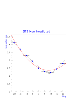
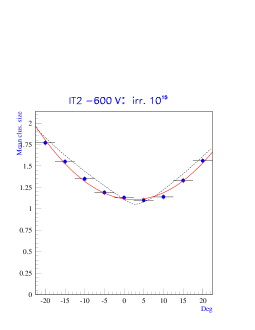
The mean cluster size as a function of the angle for not-irradiated sensor operated at 150 V is shown in fig. 1. The Lorentz angle is . In fig. 2 the distribution of the same quantity for a full-irradiated sensor is shown. The plot refers to data taken in a test beam in 1998. The corresponding Lorentz angle is . The same sensor was measured again in 1999, finding a compatible value of . An half-irradiated sensor was also tested at two different operating voltages: at 600 V as foreseen during data taking in ATLAS and at the lower voltage of 150 V for a better understanding of its behaviour. The measured Lorentz angle values were respectively and .
The expected mean multiplicity as a function of the track incidence angle was numerically calculated, using the properties and the operating conditions of the detectors under study (temperature, magnetic field, bias voltage, depletion, geometry and thresholds). This calculation is based on a model which describes charge drifting in silicon devices. To compute the drifting trajectories is necessary to know the electric field, the magnetic field and the mobility.
The Lorentz angle is given by [6]
| (1) |
where is the Hall mobility and the drift mobility. Their ratio r (Hall factor) depends on the scattering mechanism. It has a weak dependence on temperature while it does not depend on doping level as long as the doping level is below . The mobility depends on temperature and electric field. This dependence was parametrized as in [7].
Fig. 3 shows the mobility and the Lorentz angle (assuming and T) as a function of the electric field for =263 K and =300 K (irradiated and not-irradiated detectors). The markers correspond to the temperature and the mean electric field present in the detectors under study, where V is the applied voltage and d is the depletion depth.
The irradiated samples have a lower Lorentz angle because of lower mobility due to a larger electric field. Actually the electric field is not constant in the detector due to the presence of spatial charges, then Lorentz angle varies throughout the detector with the position inside the depletion zone. The track incidence angle for which the mean hit multiplicity is minimum was defined effective Lorentz angle.
The doping concentration was assumed to be uniform. This is in agreement with the scaling of depletion depth with bias voltage observed in half-irradiated detectors: the depletion approximately doubles when the voltage is increased from 150 V to 600 V. With this assumption the electric field varies linearly from the backplane to the read-out plane, both in irradiated samples , which have a p-type substrate and are partially depleted, and in not-irradiated devices which are over depleted.
The mean multiplicity for a given detector and track incidence angle was computed taking into account charge drifting, charge diffusion and threshold. Experimental results were compared with the model. The values of depletion depth used in the model were experimentally measured (see Section3). The results obtained are summarized in table 1.
3 Measurement of the Depletion Depth
The measurement of the depletion depth was performed rotating the detector around the axis parallel to the longer size of pixels. The angle between the beam direction and the normal to the sensor plane was set to or . The method is illustrated in fig 4: a cluster of contiguous pixels is activated by the beam particles crossing the detector.
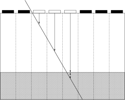
The charge collected at each pixel is proportional to the length of the track segment in the depleted area below the pixel itself. The alignment of the tracks is performed by the measurement of Time Over Threshold of the first fired pixel in the cluster. For each fired pixel in the cluster the depth of the center of the segment is calculated.
In fig. 5 the distributions of the track-segment depth are shown for a sensor irradiated to a fluence of and operated at two different values of bias voltage. The maximum depth is measured determining with a fit the point of inflexion of the track-segment depth distribution.
The consistency of the method was checked with not-irradiated sensors, that are fully depleted, for which the depletion is equal to the nominal thickness.
4 Conclusions
The Lorentz angle of ATLAS pixel radiation-hard sensors in a field of 1.4 Tesla was measured. For a not-irradiated sensor operated at 150 V a value of was found. Two different measurements for a sensor irradiated with and operated at 600 V gave the compatible values of . and . The Lorentz angle depends through the mobility upon the electric field inside sensors. The observed behaviour is well explained by a model based on charge drift in silicon. At the operating conditions for ATLAS pixel sensors a Lorentz angle of at the beginning of data taking, decreasing to after 10 years of operation, is expected.
References
- [1] The ATLAS Pixel Collaboration, ATLAS Pixel Detector Technical Design Report, CERN/LHCC/98-13, CERN 1998
- [2] F. Ragusa, Recent developments in the ATLAS pixel detector, Nucl. Instr. and Meth. A 447 (2000), 184.
- [3] M.S. Alam et al., The ATLAS silicon pixel sensors, CERN-EP/99-152, submitted to Nucl. Instr. and Meth. A
- [4] R.H. Richter et al., Nucl. Instr. and Meth. A 377 (1996) 412.
-
[5]
E. Belau et al., Nucl. Instr. and Meth. A 214 (1983) 253.
N. Bingefors et al., Nucl. Instr. and Meth. A 328 (1993) 447. - [6] W. Shockley, Van Nostrand, Princeton, N.J. (1950).
- [7] C. Jacoboni et al., Solid State Electronics 20 (1977) 77.