Two Large-Area Anode-Pad MICROMEGAS Chambers as the basic elements of a Pre-Shower Detector
Abstract
The design of a detector based on MICROMEGAS (MICRO MEsh GAseous Structure) technology is presented. Our detector is characterized by a large active area of 398281 mm2, a pad read-out with 2022 mm2 segmentation, and an uniform amplification gap obtained by insulating spacers (100 m high and 200 m in diameter). The performances of several prototypes have been evaluated under irradiation with secondary beams of 2 GeV/c momentum charged pions and electrons. We consider such a detector as the basic element for a pre-shower detector to equip the PHOton Spectrometer (PHOS) of the ALICE experiment. Its assets are modularity, small amount of material, robustness and low cost.
I Introduction
The main goal of experiments at relativistic heavy-ion colliders, like RHIC at Brookhaven and LHC at CERN, is to produce and study, in the laboratory, the primordial matter of the universe which is predicted to consist of a plasma of deconfined quarks and gluons (QGP). Among the various considered probes and related observables (strange hadrons, heavy mesons, di-electrons, etc.), direct photons will explore the partonic phase during the equilibration process, as well as the QGP phase itself [1, 2, 3]. In the ALICE (A Large Ion Collider Experiment) experiment at CERN [4], direct photons will be detected and identified with PHOS (PHOton Spectrometer) [5]. PHOS is a highly segmented electromagnetic calorimeter (EMCA) which will consist of 17280 lead-tungstate (PbWO4) crystals, associated to a charged particle veto detector (CPV). Each crystal (2.22.218 cm3, 20 radiation lengths) is coupled to a PIN-diode associated to a low noise pre-amplifier. The PHOS spectrometer will be positioned at the bottom of the ALICE magnet, 4.6 meters away from the interaction point. It will cover the pseudo-rapidity range from -0.12 to 0.12 and the azimuthal-angle domain from 45∘ to 135∘. Rejection of charged hadronic showers will be performed with the CPV detector, positioned in front of the PHOS crystals.
Recent analyses of the direct photon production in heavy-ion collisions at SPS energies [2, 3, 6] have pointed out the limits of the photon identification power resulting from two kinds of contaminations: i) the showers induced by neutral hadrons (mainly and ), and ii) the overlap of showers in high multiplicity events. These contaminations are expected to become much more severe at LHC energies. In order to properly minimize these effects, we have designed a pre-shower detector to be associated with PHOS. This detector noticeably improves the photon identification power and allows for a direct measurement of the electromagnetic shower vertex. The PPSD (PHOS Pre-Shower Detector, Fig. 1) consists of two distinct MICROMEGAS (MICRO MEsh GAseous Structure) gas counters: the Charged Particle Veto (CPV) and the Photon Conversion (PC) chambers, sandwiching a passive Pb converter.
Among the new micro-pattern detectors exploiting avalanche multiplication in narrow gaps [9], MICROMEGAS technology [10] appears as a very promising option in terms of performances, robustness, reduced amount of material, and cost (see e.g. [11, 12, 13, 14, 15, 16]). For our specific needs, we justify the choice of the MICROMEGAS technology with the following considerations:
-
1.
It provides the modularity well suited to cover areas of a few squared meters.
-
2.
It is mechanically robust and resistant to electrical discharges.
-
3.
The small lateral development of the electron cloud in the amplification gap, prevents from significant overlaps in high multiplicity events.
-
4.
The small amount of material minimizes photon-conversion and nuclear interactions within the detector.
Using our PPSD design, the identification capabilities of PHOS will be improved as follows:
-
1.
Muons will be identified as minimum ionizing particles (MIPs) in the CPV, PC and EMCA detectors.
-
2.
About half of the charged hadrons (, , K+, K-, etc.) will be detected as MIPs in the CPV, the PC, and the calorimeter. The other half of charged hadrons will develop a hadronic shower in the calorimeter.
-
3.
Photons will be unambiguously identified by three features: the absence of a hit in the CPV, a hit in the PC detector, when the photon is converted into an pair within the absorber, and an electromagnetic shower in the calorimeter. The identification efficiency will depend on the thickness of the passive converter. The optimal thickness results from a compromise between the photon identification efficiency of the PPSD and the photon energy resolution of the spectrometer. From simulations [7], we deduced that the best trade-off is achieved for a thickness equivalent to one radiation length. Additionally, from the hit position in the PC detector, the shower vertex will be directly measured, providing information to resolve the overlapping showers expected in high multiplicity events.
-
4.
Neutral hadrons will trigger most of the time nor the CPV, neither the PC detector (the intermediate Pb passive converter represents only 5% of the nuclear interaction length).
-
5.
Electrons and positrons will be identified by a hit in the CPV and PC and by an electromagnetic shower developing in the EMCA. Additional improvement of the electron and positron identification power could be achieved by considering the deposited energy in the PC detector.
In the present report, the performances of large-area anode-pad MICROMEGAS detectors, irradiated with a 2 GeV/c pion and electron beam, are presented in terms of pad response to MIP, gain in the amplification gap and detector efficiency. In addition, we have studied the electrical discharge probability per ionizing particle as a function of the detector gain, in order to probe the reliability of this technology in large multiplicity experiments. Finally, we have studied the electron and pion response functions of a pre-shower detector prototype.
II Description of a Large-Area Anode-Pad MICROMEGAS Chambers
The MICROMEGAS technology [10, 11] consists of an asymmetric two-stage parallel-plate gas-detector. The first stage, a 3 mm thick conversion gap, is separated from the 100 m thick amplification gap, by a micro-mesh foil resting on insulating spacers. The amplification gap is closed at the bottom by the pad anode surface. Such a configuration allows to establish simultaneously a very high electric field in the amplification region ( 50 kV/cm) together with a low electric field in the drift region ( 2 kV/cm), by applying suitable voltages between the three electrodes (cathode-mesh-anode). When a charged particle traverses the conversion gap, it generates primary electrons which are subsequently multiplied in the small amplification gap. The associated ion cloud is quickly collected on the micro-mesh layer generating a relatively fast signal, whereas only a small part of the ion cloud penetrates into the conversion region. The amplified electron cloud is collected on the anode providing a fast electric signal.
Based on this principle, we have developed several large-area prototypes with pad read-out (Fig. 2 and Fig. 3). The characteristics of the chambers are the following:
-
1.
Anode: The total area of the anode plane is mm2, providing an active area of mm2. The anode electrode consists of a 1.0 mm thick printed circuit board. Its inner surface is segmented in rectangular 20 22 mm2 gilded copper pads, and the signal is collected on the other side through strips to the connectors. The inter-pad width is 100 m and the total number of pads is 256. Each pad is pierced by a conductive pine hole of 300m in diameter to allow for readout through the board. The rigidity of the board is obtained by sticking an additional 3 mm thick board made of low composite material (EPOXY glass and ROHACELL). To keep the small amplification gap as uniform as possible, well-calibrated micro-spacers (100 m high and 200 m in diameter) are deposited on the pads with a pitch of 2 mm in both directions.
-
2.
Cathode: The cathode consists of a 9 m gilded copper layer, glued on a 3 mm thick plate made of composite material and sandwiched between two 300 m thick GI180 boards. The top cathode plane is glued to a 6 mm thick Plexiglas frame of mm2.
-
3.
Mesh: The original electro-formed micro-mesh*** BMC Industries, 278 East 7th Street, St. Paul, MN 55101, USA. consists of a 3 m thick grid of 22”22” made of pure Ni. The 39 m squared holes grid are outlined by a 11 m thick border of Ni in steps of 50 m, i.e. 500 LPI (“Lines Per Inch”). The optical transparency reaches 59%. The micro-mesh is stretched on the Plexiglas frame which defines the 3 mm thick conversion gap between the micro-mesh and the cathode plane.
-
4.
The micro-mesh and cathode assembly is placed on top of the micro-spacers of the anode plane. A 2 mm thick composite-material top-lid covers the whole system to ensure the gas tightness of the chamber.
-
5.
The gas mixture flows through the detector at a pressure slightly above atmospheric pressure.
-
6.
The signals of the individual pads are collected, through the metallic hole, at the backplane of the anode plane by individual strips and transported to the front-end electronics located on the two opposite sides of the detector.
-
7.
The total thickness of the detector throughout the active detection area, is 13 mm corresponding to 1.76% of .
III Experimental setup for the beam tests
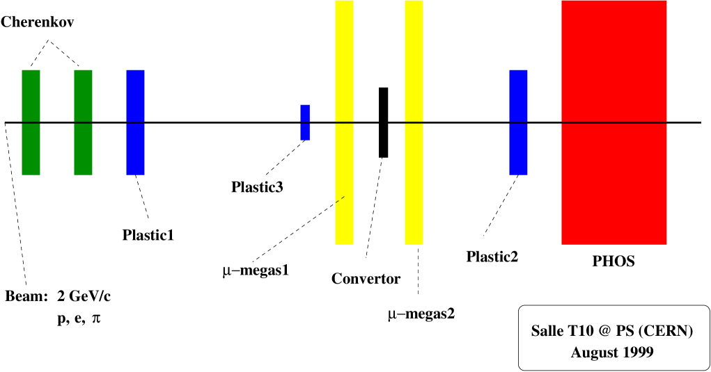
Our prototype of the PPSD detector was tested in the T10 hall at CERN (Fig. 4) The choice of the gas mixture during the experiment was Ar + 10% (isobutane). The voltage of the drift zone was fixed to = -1000 V. The basic elements of this test experiment were:
-
1.
Beam. The PS accelerator at CERN delivered a secondary beam of 2 GeV/c momentum. This beam consisted of hadrons ( 60%, mainly charged pions) and leptons ( 40%, mainly electrons). The size of the beam ”spot” was about 10 cm in diameter and the spill duration was 1 s with an inter-spill time of 9 s. The beam intensity stayed in the range of to particles per spill.
-
2.
Beam identification. Two Cherenkov detectors C1 and C2 were placed upstream of the detector to identify the impinging particles. However, only C2 (filled with CO2 at atmospheric pressure) allowed a discrimination between hadrons and leptons.
-
3.
Trigger. Two plastic scintillators (Pl1 and Pl2) with a square shape of 1010 cm2 were inserted along the beam line (Fig. 4) to define the main trigger of the acquisition. Coincidences between Pl1 and Pl2 defined a wide beam trigger. A small plastic scintillator Pl3 (11 cm2) was also included in the trigger electronics during some runs to define a narrow beam trigger. It was used to measure the MICROMEGAS detector efficiency and the background induced by the passive converter.
-
4.
MICROMEGAS detectors. Two MICROMEGAS detector prototypes were placed upstream and downstream with respect to the passive converter. Amplification of the pad signal was performed by GASSIPLEX based electronics [20]. The elemental electronics card consisted of 3 GASSIPLEX chips serving 16 channels each. These cards (6 cards per detector) were directly attached to the detector board. The GASSIPLEX sequential signal was digitized by the CAEN V550 VME ADC (up to 1024 channels). Operations on the GASSIPLEX and the V550 module were synchronized via a CAEN V551A VME sequencer.
-
5.
Passive Converter. During a few runs, a passive lead converter, 6 mm thick, covering an area of 1010 cm2 was placed in between the two MICROMEGAS chambers.
-
6.
PHOS array. An array of 88 PHOS type crystals was also placed at the end of the beam line but not used in our investigation. It is mentioned here for the sake of completeness.
IV Detector performances
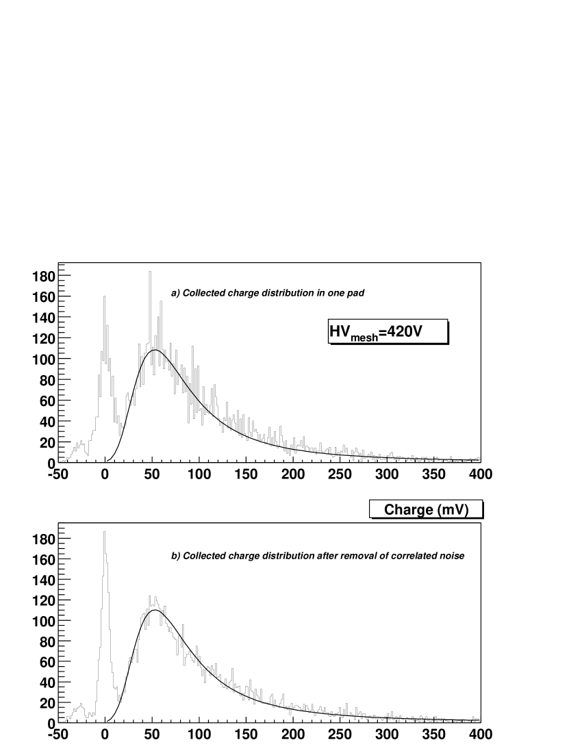
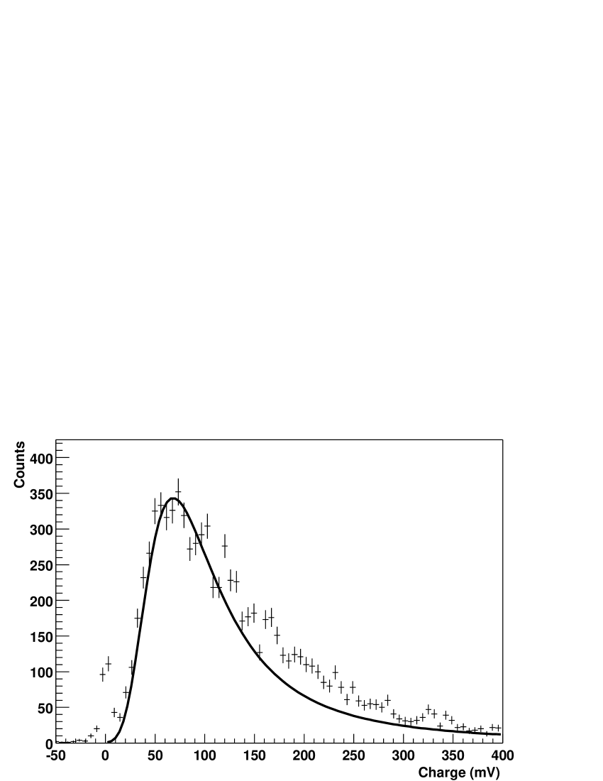
The charge distribution collected by a single pad (Fig. 5) of the MICROMEGAS chamber when considering the wide beam trigger, exhibits two components:
-
For low amplitudes (50 mV) the intrinsic electronic noise of the pad exhibits a peaked Gaussian distribution. This corresponds to events in which beam particles fire the wide beam trigger and hit one of the neighboring pads. The mean of the Gaussian distribution, , results from the intrinsic noise or pedestal. The width expressed as the standard deviation of the distribution, , results from the pad intrinsic electronic noise, which depends on the capacitance of the pad and on the electromagnetic environment.
-
At larger amplitudes, one observes the detector response to ionizing particles which exhibits the usual Landau distribution reflecting the fluctuations in the number of primary electrons created in the thin drift region. For a 3 mm gap filled with Ar+10% isobutane at atmospheric pressure, on average, about 34 electrons per MIP are created. The maximum of the Landau distribution, , reflects the gain achieved in the amplification zone and its width the average number of primary electrons (a smaller average number of primary electrons leading to larger fluctuations).
The correlated noise, a noise level common to all pad signals, adds to the intrinsic noise of a pad. It can be removed on an event-by-event basis. We defined this noise as
| (1) |
where is the number of pads with a collected charge lower than 3 times the width of the noise. After removal of this correlated noise (Fig. 5b), the charge distribution exhibits a much narrower noise peak, offering an improved discrimination of MIP particles from noise, and leading to an increase of the detector efficiency.
A Gain in the amplification gap
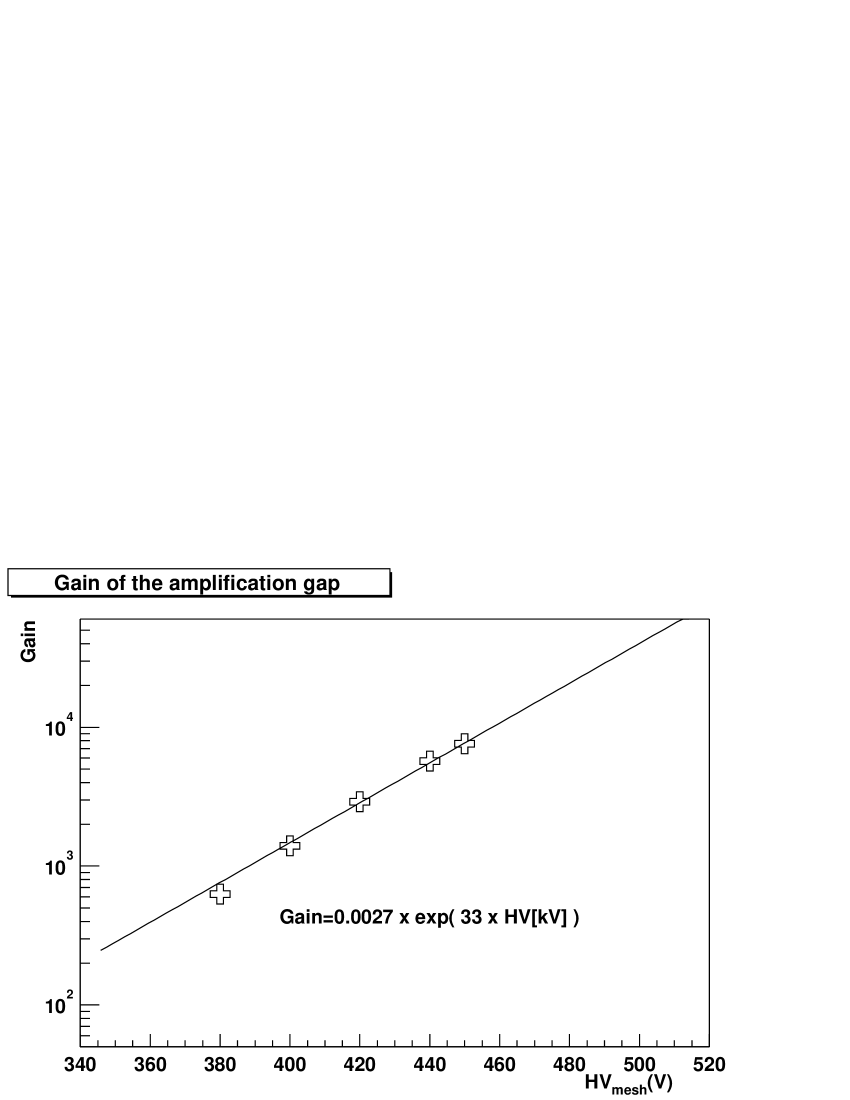
We have studied the evolution of the Landau distribution as a function of the micro-mesh voltage and for a constant cathode voltage. We observe that the position of the maximum increases with the micro-mesh voltage: an increase of 20 V changes the position of the Landau maximum by a factor 2. The total number of electrons collected at the anode pad is calculated as:
| (2) |
where and are the position of the maximum of the Landau and Gaussian distributions respectively, = 10 mV/fC is the gain of the GASSIPLEX (pre-amplifier and shaper) electronics [20], is the factor to convert the average charge from the maximum value (GEANT simulations of the energy loss fluctuations give = 2.5) and is the charge of the electron. The gain, , is calculated as:
| (3) |
where is the number of primary electrons generated in the conversion gap. The gain ranges from several hundreds to several thousands for a voltage variation between 380 and 450 V (Fig. 6). The maximum achieved gain in the amplification gap, while staying below the spark threshold, is of the order of 104.
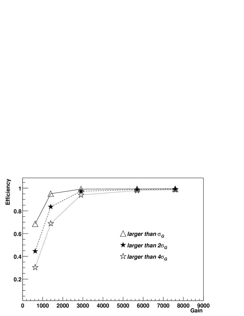
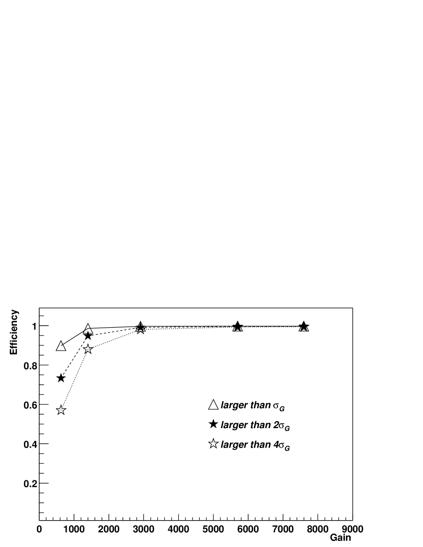
B Detector efficiency
The detector efficiency for MIPs was studied as a function of the detector gain (Fig. 7 and Fig. 8). The efficiency, , has been therefore defined as the ratio between the integrated area of the Landau distribution, starting from (where corresponds to times the noise width), and of the total integrated Landau distribution:
| (4) |
where is the induced charge in a pad. A direct measurement of the detector efficiency deduced from the events registered with the small beam trigger is in good agreement with the value deduced using the above method. For micromesh voltages larger than 420 V (i.e. ), the measured detector efficiency is larger than 95%. The steep drop of the detector efficiency for voltages below 410 V results from the fact that the gain is too low to induce a signal larger than the nominal noise dispersion. Subtraction of the correlated noise considerably improves the efficiency, and a 95% efficiency is already reached for a gain of .
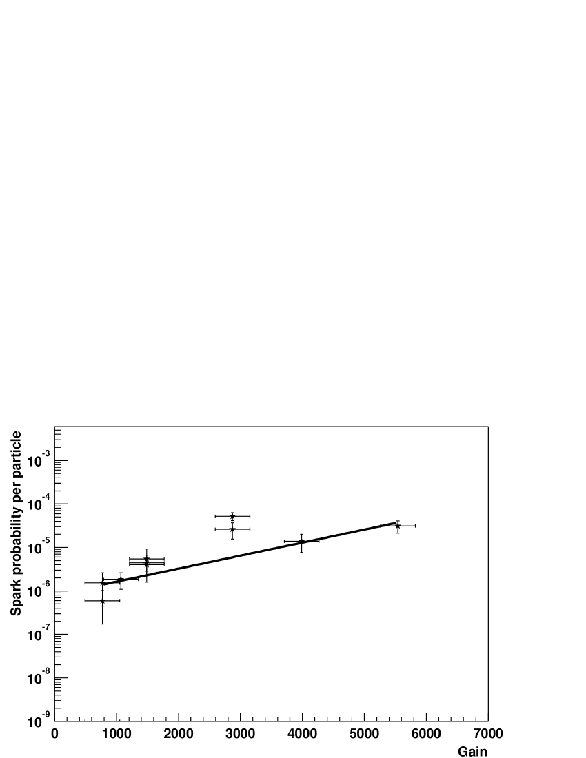
C Discharges in the amplification gap
The fundamental limitation of micro-pattern gas detectors results from the discharges induced by high particle fluxes or highly ionizing particles. Several mechanisms have been put forward to explain this breakdown process [17]. In the particular environment expected in ALICE (mainly dominated by a hadron background at low flux, below 1 Hz/mm2), the transition to a streamer regime followed by a electrical discharge occurs when the avalanche starts to contain a critical quantity of a few electrons (Raether criterion) [18]. Highly ionizing particles like alpha particles loose around 500 keV of their kinetic energy in the drift gap releasing about = primary electrons, whereas MIPs loose only around 1 keV (generating around 30 primary electrons). Alpha particles will, therefore, induce a discharge in the MICROMEGAS for gains above several (leading to larger than ). The same effect is observed when the MICROMEGAS detector is irradiated with hadron MIPs, like charged pions. In this case, nuclear interactions with nuclei of the gas mixture in the drift gap could be at the origin of the induced discharges, since a strong dependence with the average atomic number of the gas mixture has been observed [16, 19]. Although MICROMEGAS detectors are very resistant to sparks, a discharge will induce a non-negligible dead time over the whole detector active area, leading to a reduction of the effective efficiency.
We have measured (Fig. 9) the discharge probability per ionizing particle as a function of the detector gain. We obtain discharge probabilities roughly between and for different prototypes. The discharge probability does not depend on the beam intensity, as it could be expected. However, since the beam intensity was measured by Pl1 and Pl2 coincidences, impinging-particle trajectories outside of the plastic active area and passing through the MICROMEGAS detector, were not counted. This induces an asymmetric systematic error which would tend to slightly decrease the measured discharge probability.
Central heavy ion collisions at LHC will induce a flow of charged particles of the order of 50 charged particles per m2 in PHOS [5]. Taking a conservative value of 8000 central collisions per second, the charged particle rate will be of the order of 50 KHz per chamber. If the detector operates at gains of 2000 (leading to efficiencies larger than 95%), we expect a spark probability of (Fig. 9), i.e. a spark rate of 0.15 spark/chamber/second. Taking into account the fact that the dead time induced by a spark is less than 10 ms [16, 19], the dead-time induced by sparks will be as low as 0.15%. In this respect, the particle induced discharges are not a handicap of the MICROMEGAS detectors, when the chambers operate at modest gains.
In addition, recent measurements [16, 19], exhibit a strong dependence of the spark probability per ionizing particle on the average atomic number of the gas mixture, following a dependence. Therefore, selecting a gas mixture with Ne gas should lead to an additional reduction of the spark probability by more than one order of magnitude.
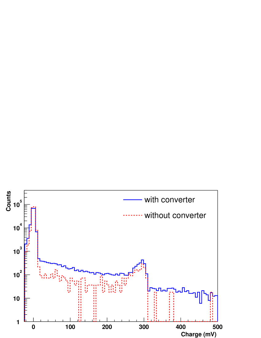
D Background induced by the passive converter
The background induced by the lead passive converter in the MICROMEGAS pad chambers has also been studied. Using the narrow beam trigger (see Fig. 10 where almost no noise peak is apparent) we have measured the charge distribution in the neighboring pads without and with the lead passive converter. We observe the following (Fig. 11):
-
without converter, 2% of MIPs induce a signal larger than the nominal noise in a neighboring pad;
-
with converter, only 6% of MIP particles induce a signal in a neighboring pad.
We conclude that the passive converter induced background is relatively small, and the detector occupancy of the MICROMEGAS pad chambers is hardly increased.
E Pre-shower response function to electrons and hadrons
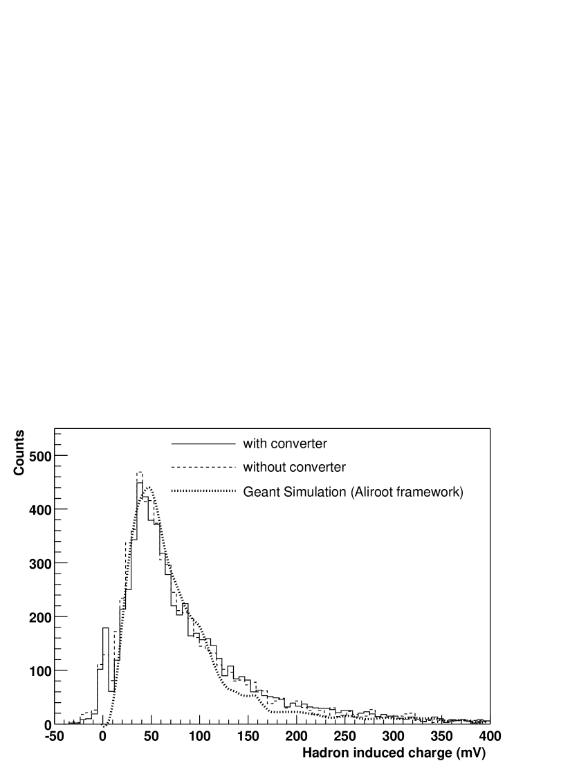
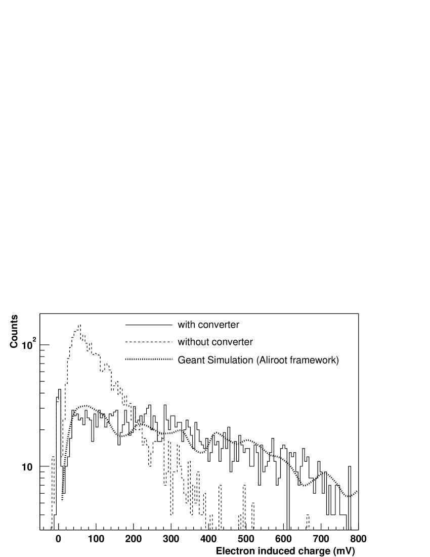
In this last section, we present the response function of the pre-shower detector to hadrons and electrons of 2 GeV/c momentum. The discrimination between the hadron and electron beam was done by means of the Cherenkov counter C2 (Fig. 4). Comparisons of the experimental response functions with the results of GEANT3.21 simulations of the pre-shower detector were also performed [7].
-
Hadron beam (Fig. 12): The PC detector exhibits almost the same Landau-like distribution with and without the converter. Fluctuations of the deposited energy in the thin conversion gas gap were calculated using the PAI model implemented in GEANT. This simulation reproduces relatively well the shape of the Landau-like distribution, although GEANT underestimates the tail of the measured distribution.
-
Electron beam (Fig. 13): Without converter, the PC detector exhibits the same Landau-like distribution observed with the hadron beam. However, by including the converter (1.07 X0) in the setup, a wider distribution is observed: on average 65% of the impinging electrons develop an electromagnetic shower inside the converter. The secondary particles produced in the shower will result, on average, in a higher energy deposit in the gas cell associated to the anode-pad leading to a broader charge distribution. GEANT3.21 simulations of the deposited energy by 2 GeV/c electrons describe rather well the observed distribution.
We conclude that the hadron response function is not significantly modified by the passive converter. However, electrons exhibit a very different response function in the presence of the passive converter, due to the initial development of electromagnetic showers. The deposited energy distribution in PC detector is wider, and this observation could be exploited to improve the electron and positron identification power of the PHOS detector.
V Conclusions and perspectives
We have developed a large-area MICROMEGAS detector with anode pads read-out. Prototypes have been irradiated with a 2 GeV/c momentum beam of electrons and hadrons. We have studied the pad response function, the gain in the amplification gap and the detector efficiency as a function of the electric field. The measured performances are in good agreement with those obtained in other MICROMEGAS developments. We have investigated the discharge probability per incident MIP particle, concluding that the induced discharges do not represent a real handicap to operate MICROMEGAS chambers in the environment expected in central heavy-ion collisions at LHC energies. A pre-shower detector design based on a sandwich of two MICROMEGAS chambers with a passive Pb converter in between, has been proven to be a promising option for the improvement of PHOS detection capabilities. The measured background induced by the converter in the MICROMEGAS chambers is very small. The pre-shower response function of hadrons and electrons presents various facets worth exploiting further. We observe that the hadron beam induces, in both gas detectors, the typical Landau-like distribution of the collected charge. The electron beam not only induces the typical Landau-like distribution in the CPV detector of the pre-shower but also exhibits a much wider charge distribution in the PC detector, signing the initial development of the electromagnetic shower.
Following the results of the tests discussed in the present article, an improved version of a PPSD has been designed. The new detector has a larger active area (380380 mm2), a thicker conversion gap (6 mm) better suited for the use of a gas mixture like Ne with 5-10% of CO2 and a 200 m amplification gap [21]. These improvements (larger amplification gap and lighter gas mixture), will lead to allow for a reduction of the spark probability by a factor 20 to 50, and therefore lead to a spark rate of 10 sparks/chamber/hour for the ALICE hadronic environment. In addition, the size of the pad has been reduced to 1111 mm2 in order to reach the spatial resolution needed to determine the shower vertex.
VI Acknowledgments
We thank M. Ippolitov and PHOS collaborators for their help during the beam test at PS (CERN). The technology for manufacturing the circuit board has been efficiently developed by A. Gandi and R. de Oliveira (CERN-EST-MT). We would like to acknowledge here the fruitful discussions with Y. Giomataris and Ph. Rebourgeard at DAPNIA (Saclay), and with P. Lautridou, L. Luquin and M. Labalme of Subatech (Nantes) during the development of the MICROMEGAS prototypes. This work was supported in part by the “Conseil Régional de la Région des Pays de la Loire”, France.
REFERENCES
- [1] Cheuk-Yin Wong ”Introduction to High-Energy Heavy-Ion Collisions”, World Scientific Publishing Company, Singapore, 1994.
- [2] R. Albrecht et al., Phys. Rev. Lett 76 (1996) 3506.
- [3] Proceedings Quark Matter 99, May 10-15 (1999), Torino, Italy. Nucl. Phys. A661 (1999).
- [4] ALICE Technical Proposal CERN/LHCC-95-71 LHCC/P3 (1995).
- [5] PHOS TDR CERN/LHCC 99-4, ALICE TDR 2 (1999).
- [6] M. M. Aggarwal et al., in preparation.
- [7] http://AliSoft.cern.ch/offline/
- [8] A. Oed, Nucl. Inst. and Meth. A263 (1988) 351.
- [9] F. Sauli, Nucl. Inst. and Meth. A419 (1998) 189.
- [10] Y. Giomataris, Ph. Rebourgeard, J.P. Robert and G. Charpak, Nucl. Inst. and Meth. A376 (1996) 29.
- [11] Y. Giomataris, Nucl. Inst. and Meth. A419 (1998) 239.
- [12] G. Charpak, Nucl. Inst. and Meth. A412 (1998) 47.
- [13] G. Barouch et al., Nucl. Inst. and Meth. A423 (1999) 32.
- [14] J.P. Cussonneau et al., Nucl. Inst. and Meth. A419 (1998) 452.
- [15] Proceedings 2nd MICROMEGAS Workshop, 24 Feb. - 5 Mars 1999, Saclay, France.
- [16] Proceedings 3rd MICROMEGAS Workshop (http://www-iphe.unil.ch/micromegas), 8 - 9 March 2000, Lausanne, Suisse.
- [17] P. Fonte, V. Peskov and B. Ramsey, IEEE 46 (1999) 321.
- [18] A. Bressan et al., Nucl. Inst. and Meth. A424 (1999) 321.
- [19] Ph. Rebourgeard, Private communication.
- [20] J. C. Santiard et al., Report CERN-ECP/94-17, 1994.
- [21] G. Martínez et al., in preparation.