Soliton electro-optic effects in paraelectrics
Abstract
The combination of charge separation induced by the formation of a single photorefractive screening soliton and an applied external bias field in a paraelectric is shown to lead to a family of useful electro-optic guiding patterns and properties.
pacs:
42.50.Rh, 42.65.Pc, 03.65.KfApart from their inherent interest as peculiar products of nonlinearity, spatial solitons hold the promise of allowing viable optical steering in bulk environments [1] [2]. Photorefractive screening solitons differ from other known manifestations of spatial self-trapping for their peculiar ease of observation and versatility [3], and recent experiments in photorefractive strontium-barium-niobate (SBN) and potassium-niobate (KNbO3) have demonstrated two conceptual applications of their guiding properties. In the first case, a tunable directional coupler was realized making use of two independent slab-solitons [4]; in the second, self-induced phase-matching was observed to enhance second-harmonic-generation [5]. Although results suggest a means of obtaining all-optical functionality, actual implementation is hampered by the generally slow nonlinear response [6], that can be ”accelerated” only at the expense of stringent intensity requirements[7]. In contrast, non-dynamic guiding structures have been observed by fixing a screening soliton [8], or in relation to the observation of spontaneous self-trapping during a structural crystal phase-transition [9]. One possible method of obtaining acceptable dynamics is to make directly use of the electro-optic properties of the ferroelectrics involved, in combination with the internal photorefractive space charge field deposited by the soliton. Since photorefractive charge-activation is wavelength dependent, one can induce charge separation in soliton-like structures at one active wavelength (typically visible), and then read the electro-optic index modulation at a different, nonphotorefractive, wavelength (typically infrared) [10] [11]. For noncentrosymmetric samples (such as the above mentioned crystals) that typically host screening soliton formation, the electro-optic index of refraction modulation is proportional to the static crystal polarization P, and thus to the electric field (linear electro-optic effect). For these, no electro-optic modulation effects are possible: for whatever value of external constant electric field Eext, the original soliton supporting guiding pattern remains unchanged. In centrosymmetrics, such as photorefractive potassium-lithium-tantalate-niobate (KLTN), solitons are supported by the quadratic electro-optic effect [12] [13] [14] [15]. In this case, the ”nonlinear” combination of the internal photorefractive field with an external electric field can give rise to new and useful soliton-based electro-optic phenomena, which we here study for the first time.
The basic mechanism leading to screening soliton formation is the following: a highly diffracting optical beam ionizes impurities hosted in the lattice of an electro-optic crystal. An externally applied electric field makes these mobile charges drift to less illuminated regions, forming a double layer that renders the resultant electric field in the illuminated region lower. For an appropriate electro-optic sample, this leads to a self-lensing and soliton propagation, when beam diffraction is exactly compensated. For slab solitons, i.e. those self-trapped beams that originate from a beam that linearly diffracts only in one transverse dimension (x), for a given soliton intensity full-width-half-maximum (FWHM) x, a given ratio between the soliton peak intensity and the (generally artificial) background illumination, (intensity ratio), solitons form for a particular value of applied external biasing field . The soliton-supporting electric field E is expressed by E=(V/L)(1+I(x)/Ib)-1, where V is the external applied voltage, L is the distance between the crystal electrodes (thus =V/L), and I(x) is the soliton optical intensity confined in the x transverse dimension [12]. This electric field, a result of a complex nonlinear light-matter interaction, is present even when the generating optical field is blocked, and the sample is illuminated with a nonphotorefractively active light. Charge separation is smeared out only by slow recombination, associated with dark conductivity, characterized by considerably long decay times. The nonphotorefractively active illumination, although not leading to any further evolution in the internal charge field, will feel the index inhomogeneity due to the quadratic electro-optic response described by the relation n =-(1/2) n3 g(-1)2E2, where n is the crystal index of refraction, is the effective electro-optic coefficient for a given scalar configuration, is the vacuum dielectric constant, and is the relative dielectric constant. The actual electric field in the crystal is now E=(V/L)(1+I(x)/Ib)-1-(V/L)+Eext, where Eext (in general ) is the externally applied electric field after the nonlinear processes have occurred (the ”read-out” field). The index pattern induced is
| (1) |
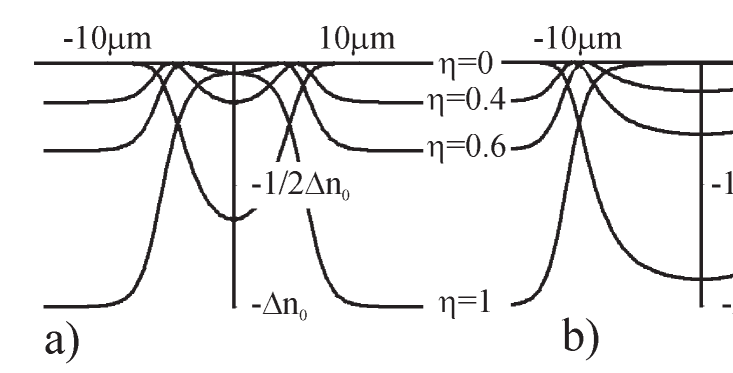
where n0 =(1/2) n3g(-1)2(V/L)2. In Fig.(1) we show two families of induced index patterns associated with two solitons at different saturation levels. In Fig.(1a) a 7m FWHM soliton at =514 nm wavelength (n5.4, for n=2.45) with an intensity ratio =4, leads to three characteristic pattern regimes: for E1, the soliton supporting potential is formed. For 0, an antiguiding hump appears, whereas for intermediate values of , a twin-waveguide potential forms. Analogous results can be predicted for a strongly saturated regime shown in Fig.(1b), where a 11m soliton is formed for 22.
Experiments are carried out with an apparatus that is well documented in literature [13] [14]. An enlarged TEM00 Gaussian beam from a CW Argon-ion laser operating at =514nm, is focused be means of an f=150mm cylindrical lens onto the input facet of an mm sample of zero-cut paraelectric KLTN, at T=20 ∘C (with a critical temperature Tc=11 ∘C), giving rise to an approximately one-dimensional x-polarized Gaussian beam of x11 m (”soliton” beam), and the entire crystal is illuminated with a second, homogeneous beam (”background” beam) from the same laser, polarized along the y axis. Both the focused and the plane-wave beams copropagate along the z-direction. The constant voltage V is applied along the crystal x direction, the crystal itself being doped with Vanadium and Copper impurities, and photorefractively active at the laser wavelength. Guiding patterns can be investigated either by illuminating the crystal with an infrared beam (as mentioned above), or simply by using the same soliton-forming wavelength, but at a lower intensity, since photorefractive temporal dynamics are proportional to beam intensity. Here we use this read-out method, and in what follows all read/write experiments are at =514nm, with Iread/I20. By changing the value of the applied readout voltage, Vext, we can explore the optical potential described by Eq.(1), through the variable . Beam distribution is investigated by imaging the facets of the sample onto a CCD camera by means of a second lens placed after the sample (along the z direction).
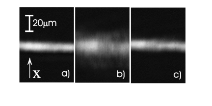
In Fig.(2) the observation of a single photorefractive screening soliton is shown. The 11m soliton is observed with an intensity ratio u 22 at Vexp=1.33 kV, annulling linear diffraction to 24 m . Soliton formation takes approximately 3 min, for an I1.8 kW/m2 (I80 W/m2), measured directly before the sample, thus meaning that erasure during readout would take, at the very least, about 1 hr (i.e. longer than the duration of any one of our experiments). Had we used an IR read-out beam, decay would be halted indefinetly. Given the sample geff=0.12m4C-2, 9000, 6.9, the expected value for soliton formation would be V1.27 kV.
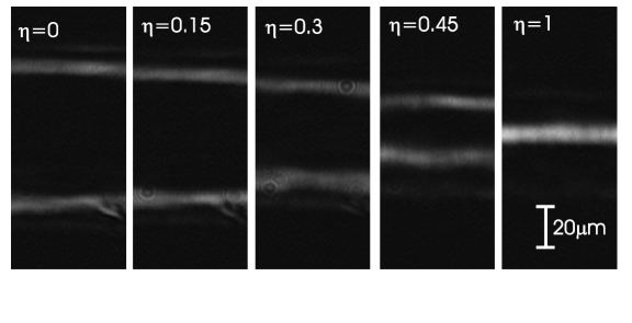
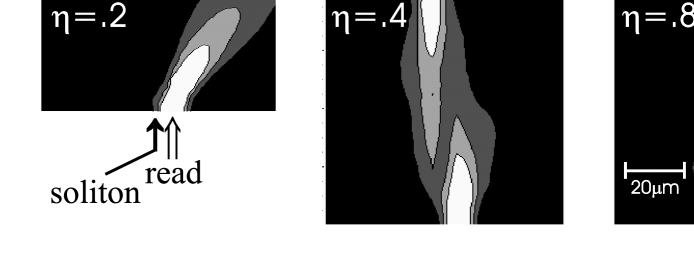
In Fig.(3) we show the same region of the crystal invested by the less intense (but otherwise identical to the soliton generating) ”read” beam at various values of . For =1 the output beam is identical to the soliton (apart from the actual intensity). For low values of (0.4) the index pattern given by Eq.(1) is antiguiding, and the output beam is scattered and split into two diffracting beams (beam ”bursting”, see Fig.(1b)). As is increased, the defocusing is weakened and for the sample gives rise to a beam-splitting on the twin-waveguide structure formed by the two-hump potential, as shown in Fig.(1). The distance between the two beams is m. As opposed to previous defocusing, in this case light is exciting a guided mode.
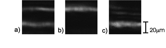
Next we shift the crystal with respect to the optical beam in the x direction, so as to launch it directly into one of the twin-guides for intermediate values of . For an = 0.45, shifting the crystal by 10m, the beam is guided by the side hump, as shown in Fig.(4b). In this forward guiding condition, we change to =0.8. The potential commutes from a double-hump twin-waveguide to a single guiding pattern (see Fig.1). The optical beam is redirected as shown in Fig.(4c).
It is therefore possible to realize, by means of the formation of a single photorefractive centrosymmetric screening soliton, three qualitatively different optical circuits: a single waveguide, a double waveguide beam-splitter, and an antiguiding beam-stopper. If the crystal is shifted so as to launch the guided beam into one of the twin-guides, it is possible to deviate the beam, maintaining its strong confinement, realizing an electro-optic switch. Had we used a longer sample, launching the beam in a twin-waveguide leads to a tunable directional coupler, as shown in Fig.(5).
The observed phenomena represent an important step in the achievement of viable soliton based components in two major aspects. The first is that the observed phenomenology occurs with the formation of a single soliton, that is only used to deposit a pattern of charge displacement (a peculiar volume hologram), whereas switching from one regime to the other occurs only through the change of the applied electric field. Thus switching dynamics are only limited by capacity charging times, as all other electro-optic devices. Secondly, whereas screening soliton formation requires a constant applied external field, during read-out, the use of independent electrodes can allow the formation of composite circuitry in cascade, all from a single soliton.
The work of E.D. and M.T. was carried out in the framework of an agreement between Fondazione Ugo Bordoni and the Italian Communications Administration. Research carried out by A.J.A. is supported by a grant from the Ministry of Science of the State of Israel.
REFERENCES
- [1] G.I. Stegeman and M. Segev, Science 286, 1518 (1999).
- [2] M. Segev and M. Stegeman, Phys. Today 51, 42 (1998).
- [3] B. Crosignani, P. Di Porto, M. Segev, G. Salamo, and A. Yariv, Riv. Nuovo Cimento 21, 1 (6) (1998).
- [4] S. Lan, E. DelRe, Z. Chen, M. Shih, and M. Segev, Opt. Lett. 24, 475 (1999).
- [5] S. Lan, M. Shih, G. Mizell, J. A. Giordmaine, Z. Chen, C. Anastassiou, J. Martin, and M. Segev, Opt. Lett. 24, 1145 (1999).
- [6] L. Solymar, D. J. Webb, and A. Grunnet-Jepsen, The physics and applications of photorefractive materials (Clarendon Press, Oxford 1996).
- [7] K. Kos, G. Salamo, and M. Segev, Opt. Lett. 23, 1001 (1998).
- [8] M. Klotz, H. Meng, G. J. Salamo, M. Segev, and S. R. Montgomery, Opt. Lett. 24, 77 (1999).
- [9] E. DelRe, M. Tamburrini, M. Segev, R. Della Pergola, and A. J. Agranat, Phys. Rev. Lett. 83, 1954 (1999).
- [10] M. Shih, Z. Chen, M. Mitchell, M. Segev, H. Lee, R. S.Feigelson, and J. P. Wilde, J. Opt. Soc. Am. B 14, 3091 (1997).
- [11] For linear schemes based on screening see A. Bekker, A. Ped’el, N. K. Berger, M. Horowitz, and B. Fisher , Appl. Phys. Lett. 72, 3121 (1998) and Ph. Dittrich, G. Montemezzani, P. Bernasconi, and P. Gunter, Opt. Lett. 24, 1508 (1999).
- [12] M. Segev and A. J. Agranat, Opt. Lett. 22, 1299 (1997).
- [13] E. DelRe, B. Crosignani, M. Tamburrini, M. Segev, M. Mitchell, E. Refaeli, and A. J. Agranat, Opt. Lett. 23, 421 (1998).
- [14] E. DelRe, M. Tamburrini, M. Segev, E. Refaeli, and A. J. Agranat, Appl. Phys. Lett. 73, 16 (1998).
- [15] A.J. Agranat, R. Hofmeister, and A. Yariv, Opt. Lett. 17, 713 (1992).