Dynamical systems as logic gates
Abstract
A scheme for logical computation using non-linear dynamical systems is presented. Examples of discrete-time maps configured as AND, OR, NAND and NOR gates are given. It is seen that the logical operations are flexible in the sense that an AND gate can be transformed into an OR gate with a simple change of a single parameter and vice-versa. Also, a NAND gate can be transformed into a NOR gate and vice-versa. It is shown, by example, that the scheme can even be extended to continuous-time flows. Since the NAND and NOR operations are universal, it is possible to implement any switching function by interconnecting blocks that realize these operations.
pacs:
05.45.-aI Introduction
In recent years, computation using non-conventional techniques has received considerable attention. Computation and information-processing techniques based on chemical, biological and quantum-mechanical phenomena have been studied. Murali, Sinha, Ditto and Munakata have proposed using clipped chaotic-dynamics for carrying out flexible computations Munakata et al. (2002); Murali et al. (2003a, b). In this paper, a simple scheme is proposed to configure any non-linear dynamical system as a logic gate. For this purpose, the qualitative change undergone by the system-dynamics at a bifurcation is exploited. The principle of construction of the AND, OR, NAND and NOR gates is demonstrated by examples. Both discrete-time and continuous-time nonlinear dynamical systems are considered.
II Computation using One-Dimensional Maps
Consider the logistic map May (1976)
| (1) |
is the control parameter, is the discrete-time and is the state of the system. Let where is a bias. and are logic inputs that take the value for logic- (false) and for logic- (true).
For the logistic map, the first period-doubling bifurcation takes place at . The second period doubling takes place at . The bifurcation diagram of the logistic map is shown in Fig. 1.
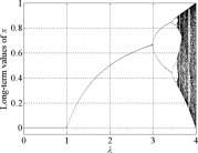
Let and in conformance with positive logic. Let us choose . Then, if both , and the map will converge to a fixed point. If either or is equal to , and the map still converges to a fixed point. However, if both , and the map settles into a 2-cycle. If the logic output is regarded as a False (logic 0) for a fixed point and a True (logic 1) for a 2-cycle, then it can be seen that the map functions as an AND gate.
If the value of is increased to while retaining the values of and , the system settles into a 2-cycle if either or both of and are true and hence we obtain an OR gate. Therefore, it can be seen that a suitable change in the parameter transforms the OR gate into an AND gate and vice-versa. The scheme is summarized as Table 1.
| Gate | ||||||
|---|---|---|---|---|---|---|
| 0 | 0 | 0 | ||||
| 0 | 1 | 0 | ||||
| 2.56 | 1 | 0 | 0 | AND | ||
| 1 | 1 | 1 | ||||
| 0 | 0 | 0 | ||||
| 0 | 1 | 1 | ||||
| 2.85 | 1 | 0 | 1 | OR | ||
| 1 | 1 | 1 | ||||
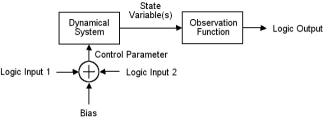
In this scheme, the logic output is defined based on the state of the system. Such a definition of the output is not in line with the output of conventional (electrical) logic gates that have two-level output signals. However, it must be mentioned that definition of input/output logic based on observed phenomena in the state of the system is not entirely new. For instance, Steinbock et al have proposed realizations of chemical-wave logic circuits wherein the binary output logic is defined by the synchronous or asynchronous nature of waves propagating through a medium Steinbock et al. (1996). For compatibility with conventional logic gates having two-level inputs and outputs, one can define an Observation Function that transforms the state of the dynamical system into a two-level signal. Note that the observation function is not essential for the system to function as a logic gate. However, if it is required to inter-connect logic gates, two-level inputs and outputs are helpful. Realizable observation functions with an appropriate level-shifting mechanism should make it possible to connect the logic output of one gate as a logic input for another. For the current example of the logistic map, an observation function can be defined to give meaningful logic output as
| (2) |
A fixed-point, with this observation function, yields zero whereas a 2-cycle yields the distance between the two points of the attractor set, which is a positive real number. Therefore, observing the output of this function is equivalent to assuming a fixed-point denotes logic 0 and a 2-cycle denotes logic 1. The scheme of implementation of a logic gate is summarized in Fig. 2.
In the preceding example, an AND/OR gate is constructed around the period-doubling from a fixed-point to a 2-cycle. In principle, the scheme should work around any bifurcation of the map. Since the behavior of the system undergoes a noticeable qualitative change at the point of bifurcation, if an observation function that differentiates between the two behaviors can be defined, the system can function as a logic gate. The bias of the control parameter ( in the preceding example) and the values of the logical inputs and can be chosen in several ways. However, the author has used the following scheme for this choice: An interval is chosen such that the critical value of the control parameter is exactly at its middle. and should respectively be chosen such that the map demonstrates the desired pre-bifurcation and post-bifurcation behaviors at these points. In the case of the preceding example, and the map undergoes a further bifurcation to a 4-cycle if , a distance of about from . Therefore, we choose the interval i.e. . We find the value . Then we take and . For operation as an AND gate, we choose and for operation as an OR gate, we choose .
III Computation using Two-Dimensional Maps
As a second example of computation using discrete-time maps, consider the Duffing’s map:
| (3) |
| (a) | (b) |
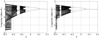
It can be noticed that the bifurcation diagrams are qualitatively different from that of the logistic map since progressive bifurcations take place with progressively decreasing values of the control parameter . This fact makes it possible to configure the Duffing’s map as a NAND/NOR gate instead of AND/OR. Analogous to the previous example, let . First, let us work with . In this case, a bifurcation from a fixed-point to a 2-cycle takes place at . Let and . As in the case of the logistic map, let a fixed-point denote false () and a 2-cycle denote true (). Then a NAND gate and a NOR gate can respectively be realized with and .
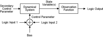
Looking at Fig.s 3(a) and 3(b), one more way of transforming the NAND gate realized at to a NOR gate becomes apparent. Instead of changing the value of , if the value of is changed to , the bifurcation from a fixed-point to a 2-cycle occurs at . If we retain , the system settles to a fixed-point if at least one of equal and the system functions as a NOR gate. Since is considered the control parameter, we refer to as the secondary control parameter. Transfer-function control of the logic gate by bias value as well as secondary control parameter is summarized in Table 2.
| Gate | ||||||
|---|---|---|---|---|---|---|
| 0 | 0 | 1 | ||||
| 0 | 1 | 1 | ||||
| 1 | 0 | 1 | NAND | |||
| 1 | 1 | 0 | ||||
| 0 | 0 | 1 | ||||
| 0 | 1 | 0 | ||||
| 1 | 0 | 0 | NOR | |||
| 1 | 1 | 0 | ||||
| 0 | 0 | 1 | ||||
| 0 | 1 | 0 | ||||
| 1 | 0 | 0 | NOR | |||
| 1 | 1 | 0 |
Variation in the critical value of the control parameter with the variation of a secondary control parameter can be seen in many 2-dimensional maps and can be used for controlling the gate’s transfer-function as seen in this example. In section IV, we shall see that such control of the transfer-function is also possible with continuous-time flows. Fig. 4 summarizes this scheme.
IV Computation using Flows
Consider the Rössler system Peinke et al. (1992); Nagashima and Baba (1999)
| (4) |
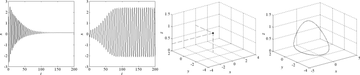
where and respectively denote the derivatives of the state-variables and with respective to time . Let and . Let be the control parameter. The system bifurcates at with fixed-point convergence for and limit-cycle for . Plots of state-variable and stationary phase-space trajectories at and can be seen in Fig. 5.
| (a) | (b) | (c) | (d) |
If a fixed-point denotes logic 0, a limit cycle denotes logic 1, and we obtain an AND gate. The bias value yields an OR gate.
Several observation functions can be defined to differentiate between the signals of Fig.s 5(a) and 5(b). For an electrical system, if is a voltage signal, a full-wave rectifier followed by a low-pass filter will give a constant DC signal for the limit-cycle case of Fig. 5(b) while giving zero output for the fixed-point case of Fig. 5(a) and can be considered a realizable observation function.
As in the case of two-dimensional maps, a secondary control parameter can also be used to control the transfer function. If is changed to , the bifurcation from a fixed-point to limit-cycle takes place at . Then, for itself, we obtain an OR gate. The configuration of the Rössler flow as a NAND/NOR gate is summarized in Table 3.
| Gate | ||||||
|---|---|---|---|---|---|---|
| 0 | 0 | 0 | ||||
| 0 | 1 | 0 | ||||
| 1 | 0 | 0 | AND | |||
| 1 | 1 | 1 | ||||
| 0 | 0 | 0 | ||||
| 0 | 1 | 1 | ||||
| 1 | 0 | 1 | OR | |||
| 1 | 1 | 1 | ||||
| 0 | 0 | 0 | ||||
| 0 | 1 | 1 | ||||
| 1 | 0 | 1 | OR | |||
| 1 | 1 | 1 |
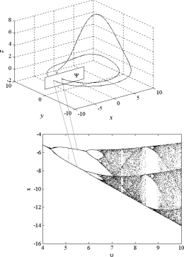
The Rössler system undergoes a series of bifurcations as is further increased. Consider the one-sided Poincaré section Parker and Chua (1987); Kapitaniak (1998) formed by the set of points at which the stationary orbit intersects the plane as changes from positive to negative. Let us denote this section plane by the letter . The Poincaré section for is shown in Fig. 6(top) and consists of only two points. Now, let be varied and at each value of the Poincaré section be determined. The abscissa (-coordinate) of each point in the Poincaré section, plotted against the corresponding value of gives the bifurcation diagram. This is shown in Fig. 6(bottom). Any bifurcation that causes a qualitative change in the behavior of the system can be used to fashion the logic-gate around.
V Concluding Remarks
It is not difficult to extend the proposed scheme to -input logic gates provided the control parameter can be split into components corresponding to one bias and the logic inputs.
In the previously proposed scheme of using clipped chaotic dynamics for logical computations Munakata et al. (2002); Murali et al. (2003a, b), it is required to modify the dynamical system by inserting a threshold-controller in the feedback path. The scheme proposed in this paper has no such requirement. Further, the threshold controller required for clipped-chaos based computation is not easy to realize as a non-electrical system. Therefore, the applications of such a scheme are likely to be restricted to electrical-realizations of dynamical systems. However, the currently proposed scheme merely requires the system dynamics to be observed and a distinction to be made between the two possible states of the system. Therefore, it is possible to employ dynamical systems of diverse physical nature - mechanical, chemical, optical, biological and fluid-dynamic systems - for information processing and computation.
Since the NAND and NOR operations are functionally complete Kohavi (1978); Tocci (1995), it should be possible to implement any arbitrary switching function by interconnecting dynamical systems that realize these logic gates. It is also interesting to note that the flip-flop, which is the fundamental digital memory element, can also be realized as an interconnection of NAND/NOR gates.
References
- Munakata et al. (2002) T. Munakata, S. Sinha, and W. L. Ditto, IEEE Trans. Circ. and Sys. - I 49, 1629 (2002).
- Murali et al. (2003a) K. Murali, S. Sinha, and W. L. Ditto, Int. J. Bifurcation and Chaos 13, 2669 (2003a).
- Murali et al. (2003b) K. Murali, S. Sinha, and W. L. Ditto, Phys. Rev. E 68, 016205 (2003b).
- May (1976) R. May, Nature 261, 459 (1976).
- Steinbock et al. (1996) O. Steinbock, P. Kettunen, and K. Showalter, J. Phys. Chem. 100, 18970 (1996).
- Peinke et al. (1992) J. Peinke, J. Parisi, O. Rössler, and R. Stoop, Encounter with Chaos (Springer-Verlag, Berlin, 1992).
- Nagashima and Baba (1999) H. Nagashima and Y. Baba, Introduction to Chaos (Institute of Physics Publishing, Bristol/Philadelphia, 1999).
- Parker and Chua (1987) T. S. Parker and L. O. Chua, Proc. IEEE 75, 982 (1987).
- Kapitaniak (1998) T. Kapitaniak, Chaos for Engineers (Springer-Verlag, Berlin, 1998).
- Kohavi (1978) Z. Kohavi, Switching and Finite Automata Theory (McGraw Hill, New York, 1978), 2nd ed.
- Tocci (1995) R. J. Tocci, Digital Systems: Principles and Applications (Prentice-Hall, Englewood Cliffs, N.J., 1995), 6th ed.