[
Structure and Stability of Si(114)-
Abstract
We describe a recently discovered stable planar surface of silicon,
Si(114). This high-index surface, oriented 19.5∘ away from
(001) toward (111), undergoes a reconstruction. We
propose a complete model for the reconstructed surface based on
scanning tunneling microscopy images and first-principles total-energy
calculations. The structure and stability of Si(114)-
arises from a balance between surface dangling bond reduction and
surface stress relief, and provides a key to understanding the
morphology of a family of surfaces oriented between (001) and (114).
(A preprint with high-resolution figures is at
http://cst-www.nrl.navy.mil/papers/si114.ps)
pacs:
PACS numbers: 68.35.Bs,61.16.Ch,73.61.Cw] The (001) and (111) surfaces of silicon are its primary growth and cleavage planes, respectively. Surfaces with orientations between these two planes are both intrinsically interesting and technologically important. For these intermediate orientations, surface morphology depends strongly on the orientation angle. For example, small misorientations away from the low-index planes produce vicinal surfaces consisting of terraces separated by steps [2, 3, 4], whereas larger angles often lead to sawtooth-like, grooved surfaces [5, 6]. Between (001) and (111), only two orientations are known to form planar surfaces with stable reconstructions: Si(113) [7, 8] and Si(5 5 12) [9]. Recently, (114) surfaces have been observed both on cylindrical Si samples [10] and within etch pits formed on Si(001) [11]. In addition, sawtooth-like structures composed of (114) and (113) facets have been observed on samples oriented between (114) and (113) [6, 10]. These results suggest that Si(114) is a planar surface that is thermodynamically stable against faceting.
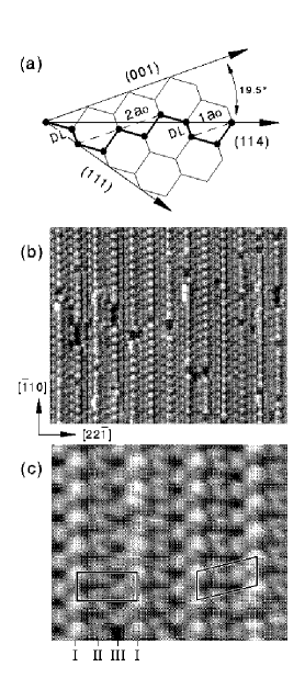
The (114) plane can be considered a highly vicinal (001) surface, oriented =19.5∘ from (001) toward (111). The structure of the ideal bulk-terminated (114) surface is an alternating sequence of one- and two-unit-cell wide (001) terraces separated by double-layer steps, as shown in Fig. 1(a). This basic terrace-plus-step morphology also describes real surfaces over a large range of orientation angles: from slightly vicinal (001) surfaces with large variable-width terraces to steeper orientations consisting of three-unit-cell wide terraces separated by double-layer steps (=11.4∘) [12]. It is interesting to ask at what orientation angle this morphology breaks down, and for what reasons. For example, the Si(113) surface (=25.2∘) has a stable reconstruction that cannot be simply described as the expected sequence of one-unit-cell terraces and double-layer steps [8]. For a surface with (114) orientation, one is therefore led to consider three possibilities: (i) a periodic surface with a terrace-plus-step morphology; (ii) a periodic surface without a terrace-plus-step morphology, similar perhaps to Si(113)-; or (iii) a non-periodic (e.g. grooved) surface. In this Letter we use scanning tunneling microscopy (STM) to definitively establish that Si(114)- is a planar surface with a stable terrace-plus-step reconstruction. We propose a complete structural model for the reconstructed surface, and use first-principles electronic-structure methods to provide strong theoretical evidence in support of this model. The structure of Si(114) reveals it to be a natural extension of vicinal (001); indeed, it marks the endpoint of a family of surfaces having closely related structure.
The clean Si(114) surface [13] appears in constant-current STM images as a well-ordered periodic array of row structures oriented along the [10] direction [Fig. 1(b)]. The period of this structure in the [22] direction is approximately 16 Å, equal to the length of the bulk-terminated (114) unit cell. Along each row, the period in the [10] direction is 7.7 Å, twice that of the bulk-terminated unit cell. Atomically resolved images reveal three distinct types of row structures, labeled I, II, and III in Fig. 1(c). The phase relationship along [10] between these row structures varies over different regions of the surface, giving rise to areas of local as well as periodicity [see Fig. 1(c)].
Our proposed structural model for Si(114)- is closely related to the structure of vicinal Si(001). The Si(001) surface undergoes a reconstruction in which the surface atoms pair up and bond to reduce the number of surface dangling bonds, forming parallel rows of dimers. For vicinal surfaces with greater than 4–5∘, the great majority of resulting (001) terraces consist of dimers oriented parallel to the step edges (B-type terraces), with these B-type terraces separated by double-layer steps ( steps) [2]. Chadi first proposed that steps are rebonded, i.e. they incorporate another row of atoms at the step edge to reduce the number of dangling bonds [14]. This basic morphology—B-type terraces separated by rebonded steps—has also been observed in STM studies of curved Si samples having regions with local orientation 9–11∘, where the (001) terrace width is only three or four unit cells [12]. We propose that a variant of this basic morphology also describes the very narrow terraces found on Si(114). Specifically, our structural model for Si(114)-, shown in Fig. 2, is an alternating sequence of single- and double-width B-type (001) terraces, separated by rebonded steps (stepping up from the double-width terrace) and non-rebonded steps (stepping down from the double-width terrace). The presence of both rebonded and non-rebonded steps provides an important mechanism for stress relief within the unit cell, as discussed in detail below.
This structural model is strongly supported by the results of first-principles calculations of equilibrium surface geometry and surface energy, and the resulting simulated STM images. The calculations were performed in a supercell slab geometry (inversion symmetric) with ten layers of Si and a vacuum layer equivalent to six Si layers. Full structural relaxation was performed using the Corning electronic-structure code of Allan, Teter, and Payne [15], which solves the Kohn-Sham equations in the local-density approximation (LDA) with a plane-wave basis and norm-conserving pseudopotentials [16]. The kinetic-energy cutoff was 10 Ry, and a single -point was used throughout. Structural relaxation was performed on all the atoms until the rms force was less than 0.1 eV/Å[17].
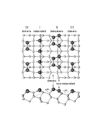
The fully relaxed surface geometry for our proposed model includes three prominent row structures per unit cell, corresponding to the three types of rows seen in the STM images. Row I in the images arises from the line of rebonding atoms at the rebonded step edge; row II arises from the row of tetramers (i.e. the combination of the dimers on the double-width terrace and the non-rebonded step-edge atoms); and row III arises from the dimers on the single-width terrace. The correspondence between theory and experiment is examined in detail in Fig. 3. Figs. 3(a) and (b) show STM images for filled and empty states, respectively, from the same surface area; Figs. 3(c) and (d) show numerically simulated STM images (constant current surfaces) calculated by integrating the local-state density over filled and empty states, respectively, near the Fermi level. In the filled-state STM image [Fig. 3(a)], rows I, II, and III all show 2 periodicity along [10] (=3.84 Å is the surface lattice constant): rows I and III each appear as an array of maxima with 2 spacing, whereas row II has a more variable appearance. In the empty-state image [Fig. 3(b)], all three rows also exhibit 2 periodicity, but the features are more diffuse within each row.
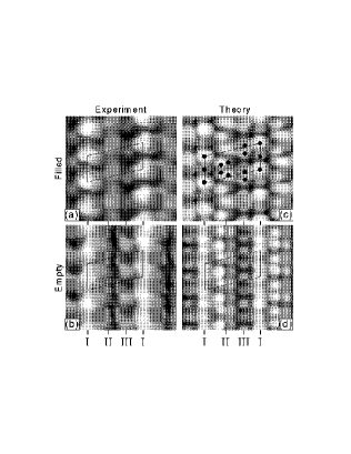
The general appearance of the rows is accurately reproduced in the simulated STM images based on our model. In the simulated filled-state image [Fig. 3(c)], row I is most prominent, and the expected 2 periodicity is apparent in all three rows, in good agreement with the STM data. Along row I, weak maxima are visible between the dominant peaks spaced 2 apart; these maxima are only occasionally resolved in STM images. Row II has a zigzag-like internal structure, consistent with the variable appearance observed experimentally. In the simulated empty-state image [Fig. 3(d)], the 2 periodicity is still evident in row II, but is much weaker in rows I and III, as observed in the experimental image. Finally, the experimental observation of areas with local and symmetry is also consistent with our model. We have calculated total energies of both reconstructions and find differences only at the level of 1–2 meV/Å2.
Several of the topographic features described above are a consequence of a structural distortion that occurs within each row. For example, at equilibrium the dimers that constitute row III are each tilted (buckled) so that the two dimer atoms have a theoretical height difference of =0.17 Å. This buckling occurs on flat Si(001) as well, and is energetically favored by the transfer of an electron from the lower to upper atom of the dimer. A similar buckling occurs along the line of rebonding atoms that constitute row I (=0.18 Å). Both of these bucklings, although small, give rise to a large corrugation of the constant-current surfaces and are critical to explaining the appearance of rows I and III as lines of maxima with 2 spacing. The tetramers, which constitute row II, have a more complicated geometry that gives rise to the internal structure visible in both the experimental and simulated images. In the equilibrium surface geometry shown in Fig. 2, the tetramers are essentially symmetric (no buckling). In the course of relaxing from slightly different initial geometries, however, we found a variation on this structure (also at equilibrium and with essentially the same total energy) with a highly buckled tetramer (=0.30 and 0.15 Å for the dimer pair and step-edge atom pair, respectively). The simulated images in Fig. 3 are from a surface with buckled tetramers; the similar total energies suggest the possibility of different metastable geometries within row II, explaining its variable appearance in the experimental images.
Experimentally, we observe that Si wafers oriented within 0.5∘ of (114) form large terraces of (114) separated by steps. Wafers with orientations a few degrees off (114) toward (111) form grooved surfaces consisting of (114) and (113) facets [18], consistent with earlier x-ray scattering results [6] and ex-situ atomic force microscopy [6]. These observations suggest that the surface energy of (114) is quite low, perhaps comparable to Si(113)-. We have investigated the stability of our Si(114)- reconstruction model, relative to low-index reconstructed surfaces, by calculating surface energies, . Here is the total energy of the supercell containing atoms, is the total energy per atom of bulk Si (computed using the same lattice vectors, energy cutoff, and zone sampling as for the surface calculations), and the factor of two accounts for the two surfaces per unit cell. We find the surface energies for the fully relaxed reconstructions of Si(111), (001), and (114) to be 84, 86, and 85 meV/Å2, respectively, indicating that Si(114)- is approximately as stable as the low-index (111)- and (001)- surfaces.
While our proposed model—a terraced surface with steps alternately rebonded and non-rebonded—was guided by our STM results, we have also carried out fully relaxed total-energy calculations for a number of alternative structures. All lead to simulated STM images in strong disagreement with experiment, and most lead to significantly higher surface energies than our proposed model. Two of these models, however, shed light on the mechanism that ultimately stabilizes Si(114): (Model A) a terraced surface with every step rebonded; and (Model B) a terraced surface with every step non-rebonded. Because rebonded steps have fewer surface dangling bonds than non-rebonded steps, one might naively predict Model A to be strongly favored relative to both Model B and our model. When fully relaxed, however, we find that Model A has a surface energy of 87 meV/Å2, very slightly higher than our model (Model B is significantly higher, at 97 meV/Å2).
We believe that the alternation of rebonded and non-rebonded step edges is ultimately favored because it leads to an optimal balance between surface dangling bond reduction and surface stress relief. For isolated steps on Si(001), rebonded steps are energetically preferred to non-rebonded steps because the number of dangling bonds is reduced. However, rebonded steps contribute a tensile stress in the direction perpendicular to the step edge. For sufficiently wide terraces, this stress is elastically relieved, so that rebonded steps are favored. For very short terraces, however, this relief mechanism is not available, and the resulting energy penalty may be larger than the energy gain from dangling-bond reduction. Si(114) balances these competing effects by incorporating both a rebonded and a non-rebonded step in each unit cell, allowing for both dangling-bond reduction and stress relief within the unit cell.
This mechanism of stress relief can be demonstrated quantitatively by calculating the LDA surface stress tensor for each model, , where is the surface strain tensor and is the surface cell area [19]. Based on the above arguments, for Model A one expects a large tensile stress in the -direction (i.e. perpendicular to the step edge), whereas for Model B and our model one expects a smaller (compressive or tensile) stress. Indeed, we find the values of to be 0.27 eV/Å2 (tensile) for Model A, 0.03 eV/Å2 (compressive) for Model B, and 0.11 eV/Å2 for our model. These numerical results are consistent with the qualitative scenario described above: Model A has a low density of dangling bonds but high surface stress, which incurs a large energy penalty; Model B has a low surface stress but high density of dangling bonds, which also incurs a large energy penalty. Our proposed model compromises on both dangling bonds and surface stress, and by so doing is the most favorable.
The competition between the energy gain from dangling-bond reduction and the energy penalty from tensile stress at rebonded steps provides a framework for understanding the surface morphology of a surprisingly large class of orientations, from slightly vicinal Si(001) up to Si(114) (=19.5∘). For orientations up to (114), the stress at rebonded steps can be relieved either on the terraces or by the presence of non-rebonded steps, and consequently the terrace-plus-step morphology is favored. For example, curved surfaces with local (119) and (117) orientations (=8.9∘ and 11.4∘, respectively) form well-ordered B-type terraces separated exclusively by rebonded step edges [12, 20]. Moreover, planar surfaces with (115) orientation (=15.8∘) consist of a complicated arrangement of B-type terraces separated by both rebonded and non-rebonded steps [18]. Beyond (114), however, the terraces become too narrow to afford sufficient stress relief, and so the terrace-plus-step morphology is no longer favored, leading to fundamentally different surface morphologies. For example, surfaces with orientations between (114) and (113) form mesoscale sawtooth-like grooves [6, 10], and surfaces with (113) orientation are stabilized by a more complex reconstruction [7, 8]. We therefore conclude that Si(114) marks the endpoint of a family of orientations, each member of which has a related surface morphology consisting of (001) terraces separated by steps.
Computational work was supported by the Cornell Theory Center and by a grant of HPC time from the DoD Shared Resource Center MAUI. Some computational results were obtained using the software program PlaneWave (Biosym Technologies). This work was funded by ONR and an NRL/NRC postdoctoral fellowship (AAB).
REFERENCES
- [1] Electronic address: erwin@dave.nrl.navy.mil
- [2] B. S. Swartzentruber, N. Kitamura, M.G. Lagally, and M.B. Webb, Phys. Rev. B 47, 13432 (1993).
- [3] O.L. Alerhand et al., Phys. Rev. Lett. 64, 2406 (1990).
- [4] E.D. Williams and N.C. Bartelt, Science 251, 393 (1991).
- [5] A.A. Baski and L.J. Whitman, Phys. Rev. Lett. 74, 956 (1995).
- [6] S. Song and S.G.J. Mochrie, Phys. Rev. B 51, 10068 (1995).
- [7] J. Knall et al., Phys. Rev. Lett. 66, 1733 (1991).
- [8] J. Dabrowski, H.-J. Müssig, and G. Wolff, Phys. Rev. Lett. 73, 1660 (1994).
- [9] A.A. Baski, S.C. Erwin, and L.J. Whitman, Science 269, 1556 (1995).
- [10] T. Suzuki et al., Surf. Sci. 298, 473 (1993).
- [11] D.L. Kendall et al., Optical Engineering 33, 3578 (1994).
- [12] M. Hanbücken, B. Röttger, and H. Neddermeyer, Surf. Sci. 331-333, 1028 (1995).
- [13] The experiments were performed in ultrahigh vacuum (UHV) with Si wafers oriented to within 0.5∘ of (114). The chemically precleaned samples were mounted on a button heater in UHV, flashed to 1150 ∘C for 60 s (pressure Torr), and then slowly cooled (see Ref. [5]). This procedure resulted in contaminant-free surfaces with well-ordered terraces greater than 0.1 m 0.1 m (determined only by the wafer miscut).
- [14] D.J. Chadi, Phys. Rev. Lett. 59, 1691 (1987).
- [15] M.P. Teter, M.C. Payne, and D.C. Allan, Phys. Rev. B 40, 12255 (1989).
- [16] M.P. Teter, Phys. Rev. B 48, 5031 (1993).
- [17] These values for supercell size, energy cutoff, zone sampling, and relaxation tolerance give relative surface energies with an uncertainty of about 1 meV/Å2.
- [18] A.A. Baski, S.C. Erwin, and L.J. Whitman, unpublished.
- [19] R.D. Meade and D. Vanderbilt, in Atomic Scale Calculations in Materials Science, edited by J. Tersoff, D. Vanderbilt, and V. Vitek (MRS, Pittsburgh, 1989), p. 451.
- [20] Curved surfaces consisting of (112), (113), (115), and (117) facets are also discussed in D.P. Adams and S.M. Yalisove, in Mechanisms of Thin Film Evolution, edited by S.M. Yalisove et al. (Mat. Res. Soc., Pittsburgh, 1994), p. 35.