The ATLAS Pixel Project
Abstract
The ATLAS experiment at the Large Hadron Collider will incorporate discrete, high-resolution tracking sub-systems in the form of segmented silicon detectors with 40MHz radiation-hard readout electronics. In the region closest to the interaction point, the thin silicon tiles will be segmented into a pixel geometry providing two-dimensional space-point information. The current status of the ATLAS pixel project will be presented with an emphasis on the performance of the front-end electronics and prototype sensors.
I Introduction
The ATLAS experiment [1] at the CERN Large Hadron Collider will function as an exploratory tool for the Higgs boson along with possible new physics phenomena beyond the scope of the Standard Model such as supersymmetry. An average of 23 minimum-bias events will be produced every 25ns at the design luminosity ( = 1034cm-2s-1). Hence interesting signatures will be buried amongst extraordinary degrees of background. In order to realise fully the physics potential of 14TeV collisions at this luminosity, ATLAS must be capable of high-efficiency track reconstruction with excellent impact-parameter resolution for 3D-vertexing and b-tagging. Even at lower luminosities of 1033cm-2s-1, ATLAS will encounter millions of pairs per year for top-quark analyses along with a plethora of -quarks enabling the possibility of CP-violation studies in the -sector. For these areas of study, the tracking system must again deliver high spatial precision and reconstruction efficiency along with excellent momentum resolution.
In addition to the performance requirements, the extremely harsh radiation environment defines perhaps the greatest challenge of all to the detector elements in ATLAS. At a radius of 30cm in the barrel region we expect to encounter a hadronic fluence***expressed in terms of the 1MeV-neutron NIEL equivalent damage of 1.310cm-2 after 10 years of operation. At 10cm the figure is closer to 1.010cm-2.
The Inner Detector of ATLAS [2] will incorporate high-resolution, low mass discrete tracking components in the form of silicon microstrip and silicon pixel [3] detectors. The pixel elements will form the innermost layers by virtue of their higher granularity and because they are more suited to providing pattern recognition capability at the greatest track densities. Also, having a greater degree of segmentation than their strip-geometry counterparts naturally endows them with lower noise-per-channel and greater immunity to radiation damage.
II Layout of the Pixel System
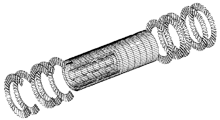
Figure 1 shows the relative positioning of the individual modules within the pixel sub-detector. There are 3 barrel layers at radii of 4.3, 10.1 and 13.2cm along with 5 disc structures which extend to 78cm in the forward directions; providing pseudorapidity coverage to 2.5. The innermost barrel layer, (known as the -layer), is not expected to survive the 10-year duration of the experiment and will therefore be replaced periodically. A single module comprises a silicon sensor tile with 16 front-end readout chips bump-bonded to it along with one Module Controller Chip (MCC). The pixel detector will incorporate 2228 such modules with a total active area of 2.3m2.
III Module structure and hybridization
There are currently two technology options being pursued for module hybridization known as the flex-hybrid approach and the MCM-D technique†††Multi Chip Module - Direct.. The former incorporates a thin kapton hybrid which is glued to the sensor backplane to provide the necessary bussing between the FE-chips, MCC and optical transmission components. The front-end chips, which are bump-bonded to the opposite face of the sensor, protrude along the long-edges of the module in order that their 48 power,data and control bond-pads may be wire-bonded up to the hybrid. The MCC sits on top of the hybrid along with the other electrical components such as decoupling capacitors, optical-link termination devices and temperature sensor.
The MCM-D method eliminates the need for wire bonds as the bussing is processed on to the sensor surface (active-side) in four layers of copper metallisation. The long sensor dimension is extended to provide a region of ‘dead’ silicon upon which the MCC and peripheral components are mounted. The sensor is also wider in order that the connections from the front-end chips to the power and control bus’ may be formed using bump-bonds in the same way that the individual pixel implants are connected to the preamp inputs.
Bump-bonding at 50m pitch was until recent years considered to be a serious issue. However, there are several vendors with whom very promising experience has been gained recently in both the Indium and -solder technologies with pre-flip-chip yields of order 10-5. For the Indium process, the flip-chip stage involves pressing together the electronics chip and sensor, (both of which have the bumps grown on them), to form a cold weld. Solder bumps are grown only on the electronics surface using a plating and re-flow technique. The recipient sensor surface is plated with a wettable metallisation. Flip-chipping in this case involves bringing the two surfaces into accurately aligned contact and re-flowing the solder at 250C.
IV Prototype Sensors
The pixel sensors will be formed from 250m-thick high- Silicon except within the -layer where it is hoped to utilise material as thin as 200m. High- silicon which begins as -type inverts to -type after a hadronic dose of 2.510cm-2. Beyond this dose the depletion voltage rises as the effective carrier concentration continues to increase. After 10-years of radiation exposure, the required reverse-bias voltage for full depletion of the pixel sensors will be in excess of 1000V. Since the maximum operating voltage is specified to be 600V, we will be forced to operate them in a partially-depleted regime. For this reason all of the prototype designs are based on -type pixel implants so that post-inversion, the junction resides on the active side.
The first-phase of sensor prototyping was conducted with two vendors; Seiko in Japan and C.I.S. in Germany. Identical wafer designs were submitted to both and featured two full-size tile designs. One of these had p-stop isolation structures, (known as ‘Tile-1’), whilst the other, (Tile-2), used the p-spray [4] technique to over-compensate the electron accumulation-layer which otherwise has the effect of shorting -implants together. Along with these devices there were a variety of smaller detector designs with a pixel-array corresponding to that of a single readout chip. Some of these matched the Tile-1 and Tile-2 designs (known as ST1 and ST2 respectively). Figure 2 shows the layout of these two designs in detail. The ST1 design is on the left and the -type isolation rings may be seen surrounding the -pixel implants. In the ST2 design there are also ring-like structures around each pixel but these are now -type and have the purpose of reducing the inter-pixel capacitance. The ST2 design also incorporates reach-through biasing which is not possible to implement with p-stop isolation.
The third design shown in figure 2 is known as SSG‡‡‡Single Small Gap. This also utilises p-spray isolation but does not include any intermediate structures. Neighbouring pixels rather have just small gaps between them.
V Front-End Readout Electronics
There are many demands on the front-end readout electronics. Insensitivity to the changes in transistor thresholds and transconductance brought on by a total ionising dose of 30MRad, (in layer-1 after 10-years of operation), must be built into the design. In addition, the front-ends must be able to deliver high-efficiency performance when the operation of the sensors has been compromised by hadronic damage. This will involve leakage-current tolerence to the level of 100nA/channel whilst maintaining sensitivity to charge spectra much reduced by partial-depletion operation and charge-trapping effects. The power consumption must not exceed 40W per channel, the timewalk must be contained to the 25ns bunch-crossing period of the LHC and the cross-coupling between neighbouring pixels should account for a charge loss of no more than 5%.
Over the last year and a half, the demonstrator development programme has followed two concurrent design directions. The two designs, known as FE-A and FE-B, were aimed at the DMILL and Honeywell radiation-hard process’ respectively. To date both have been realised in radiation-soft technologies, (namely AMS and HP), and evaluated extensively in laboratory and testbeam environments. The FE-A design, (which was initially a BiCMOS design), was also laid out and fabricated as a pure CMOS chip which is referred to as the FE-C. The two design efforts have joined forces and are now on the threshold of the first radiation-hard submission (to DMILL), of a common demonstrator design, (FE-D), which is largely based on combined features of the FE-A and FE-B approaches. Later in 1999 it is planned that a common design submission also be made for the Honeywell SOI process (FE-H). All of the demonstrator chips were designed to be fully pin-compatible enabling a common hardware test system to be used for all cases. Only minor software and firmware options are required to switch between different chips.
There were several philosophical operational differences between FE-A and FE-B not least of which was the use of a dual-threshold discriminator for the FE-B front-ends as opposed to the faster single discriminator approach used in FE-A. Time information is derived from a lower time-threshold whilst the upper threshold is resposible for hit-adjudication. Both approaches incorporate negative polarity preamps for the in sensors, LVDS inputs and outputs for clock and control lines, a serial command protocol and serial readout scheme for line reduction and local data storage in the form of end-of-column-pair buffer sets and a FIFO for hits which have matched incoming triggers. They also both incorporate eight 8-bit local DACs for front-end biases, a local chopper circuit for calibration charge injection, 7-bits of digital charge measurement based on time-over-threshold, channel-by-channel masking capability for separate strobe and readout selection and a 3-bit local threshold-tuning DAC, (TDAC), in every pixel cell for threshold-dispersion reduction.
VI Results from demonstrator-assembly testing
Throughout 1998 the collaboration followed a rich program of testing of ‘single-chip assemblies’ which comprised the radiation-soft demonstrator electronics bump-bonded to the first-generation prototype sensors, (both irradiated and non-irradiated samples). Testing has also progressed on a smaller number of full-scale modules with 16 FE readout-chips connected to a single tile.
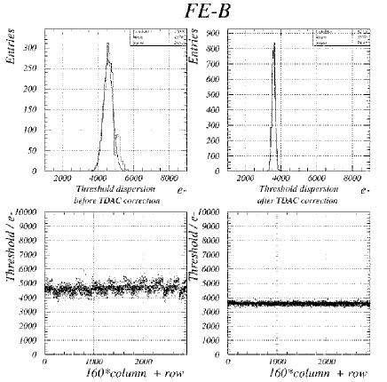
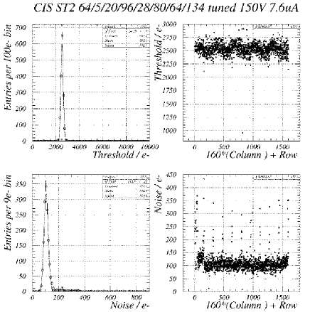
The top-left plot in figure 3 shows the distribution of thresholds for a bare chip. This is formed from scanning the input calibration-pulse amplitude in fine steps and deriving an ‘s-curve’ of efficiency versus charge (knowing the magnitude of the calibration capacitance) pixel-by-pixel. The width of this distribution is 265e- with all of the 3-bit TDACs set to the same value. On the right of this plot the TDAC values for all channels have been assigned in order to minimise the dispersion. This process results in a post-tune distribution width of 94e-.
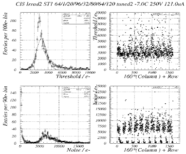
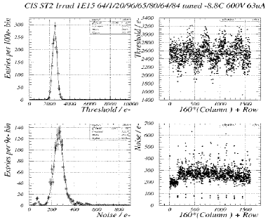
The two lower plots on the left of figure 3 show the threshold values plotted according to ‘channel-number’ which is defined to be 160column number + row number. The four rightmost plots show the tuned-threshold distribution and noise distribution for a typical FE-B single-chip assembly incorporating an ST2 sensor. The equivalent noise charge (ENC) is measured to be 105e-. Similar results are obtained for ST1 assemblies whereas the noise for an SSG device was measured to be 170e- due to the higher load capacitance.
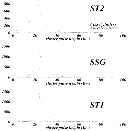
A range of assemblies were evaluated in the H8 testbeam of CERN’s SPS accelerator during four periods of 1998 running. The H8 facility offers a four cross-plane silicon microstrip hodoscope, providing an extrapolation resolution of 3m for charged pions with momenta in excess of 100GeV/c. This enabled detailed studies of hit-efficiency, charge-collection efficiency, resolution and noise occupancy to form part of the comparative process for the different prototype sensor designs both before and after irradiation. The left-most plots in figure 4 show the charge spectra obtained from the three principal design types, ST2, SSG and ST1 for tracks of normal incidence. Each plot has two histograms, one corresponding to the case where only a single channel was seen to fire and the other for double-channel clusters. In all cases except for ST2, the spectra show the usual Landau/Gaussian-convolution shape, peaking at around the 21,000e- value expected for the 280m thickness of Silicon. For the ST2 case the double-channel distribution has a distinctly lower peak value indicating some degree of charge-loss. In the central plots, a mean-charge surface is plotted as a function of the local extrapolation point within a 2-pixel cell.
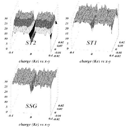
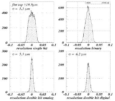
For the ST1 and SSG cases it is clear that there is a slight degree of charge-collection inefficiency in the region between neighbouring columns. For the ST2 design, the loss is extreme in this region and further loss is apparent all around the pixel-cell outline. This effect is directly attributable to the atoll -rings which surround each pixel in the ST2 design. The leftmost plots in figure 5 show residual distributions for an SSG assembly for tracks of normal incidence. The upper right distribution corresponds to the overall binary case in the dimension which yields an r.m.s. of 12.9m. This is slightly better than the expected 50m/ due to a small admixture of double-channel clusters. Similar results were obtained for all of the designs pre-irradiation.
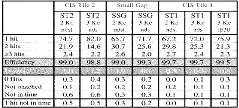
The table overleaf summarises the overall efficiency figures obtained for the ST1, ST2 and SSG assemblies for thresholds of approximately 2ke- and 3ke-. The values are at least equal to 99% in almost all cases upon application of a range of quality cuts in time and space, the single exception being ST2 at 3ke- threshold which registers 98.8%. This is due to the worse charge-collection efficiency mentioned earlier.
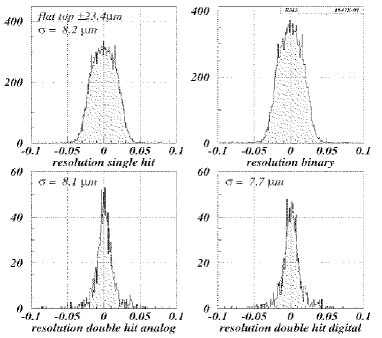
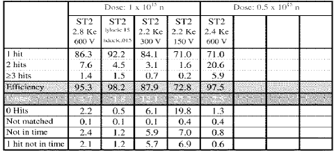
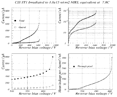
Irradiated ST1 and ST2 samples were also tested in H8 at -10C. ST2 samples which had received 5.010cm-2 and 1.010cm-2 both performed extremely well for various reverse-bias voltages up to 600V, as tabulated in the right-hand table below. An efficiency of 98.2% was recorded for the maximum dose sample when the analysis was restricted to a region within each pixel cell which eliminates the charge-loss effects due to the atoll structures. The fake-occupancy probability for this device was recorded to be 0.910-7 and half of those ‘hits’ were identified as originating from physics. On the right of figure 5 are the distributions of residuals for the high-dose ST2 sample. The overall binary resolution is measured to be 16.5m. The corresponding ST1 irradiated samples in contrast showed poorer performance. Extremely large numbers of noise hits were recorded for even the 510cm-2 sample for applied detector biases in excess of 10V.
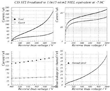
Noise analyses of the irradiated ST1 samples in the laboratory indicate severe micro-discharge occurance once the backplane bias is raised much above 100V. At 250V a broad spectrum of noise values are recorded up to 15,000e-. Even the highly dosed ST2 assembly on the other hand yields a very tight noise distribution at 600V in the laboratory with a mean of just 260e-, (see figure 7).
Figure 8 shows the results of I-V characterisations of the high-dose irradiated samples. The ST1 assembly breaks down at an applied bias of around 630V whereas the ST2 device shows no signs of breakdown even up to 1kV. All of these results strongly reinforce the view that p-spray isolation leads to lower surface fields than the p-stop approach and thus greater micro-discharge and breakdown immunity when operated at high-voltage. The next generation sensor prototypes reflect these observations with the principal design based on p-spray isolation without any intermediate structures. This design looks like the SSG approach except that the gaps are made slightly wider in order to optimise the noise performance.
VII Conclusions
The ATLAS Pixel demonstrator program is progressing well with very encouraging results obtained from radiation-soft versions of the front-end readout electronics. The success of the electronics program has enabled evaluation of a series of prototype sensor designs which have provided the collaboration with a clear concept for a new prototype layout. This new design is optimised for high-voltage operation post-irradiation whilst maintaining good charge-collection efficiency. The experience obtained with the two front-end design concepts (FE-A and FE-B) has been of great benefit in converging on combined designs for the upcoming radiation hard submissions.
REFERENCES
- [1] ATLAS Technical Proposal CERN/LHCC/94-43 (1994).
- [2] ATLAS Inner Detector Technical Design Report CERN/LHCC/97-16 (1997).
- [3] ATLAS Pixel Detector Technical Design Report CERN/LHCC/98-11 (1998).
- [4] T.Rohe et al., Nucl. Inst. Meth. in Phys. Res. A, 224-228 (1998).