A 16-channel Digital TDC Chip with internal buffering and selective readout for the DIRC Cherenkov counter of the B A B AR experiment
Abstract
A 16-channel digital TDC chip has been built for the DIRC Cherenkov counter of the BaBar experiment at the SLAC B-factory (Stanford, USA). The binning is 0.5 , the conversion time 32 and the full-scale 32 . The data driven architecture integrates channel buffering and selective readout of data falling within a programmable time window. The time measuring scale is constantly locked to the phase of the (external) clock. The linearity is better than 80 rms. The dead time loss is less than 0.1% for incoherent random input at a rate of 100 on each channel. At such a rate the power dissipation is less than 100 . The die size is 36 .
LPNHE 99-02
1 Introduction
The circuit was built for the ring imaging Cherenkov counter (the DIRC) of the B A B AR experiment[1] presently under construction at SLAC (Stanford Linear Accelerator Center) around the interaction point of the PEP-II collider[2] to observe CP violation in the decays of mesons. The accelerator is an asymmetric collider with beam energies of 9 (electrons) and 3.1 (positrons). The most recent review of the physics prospects of the B A B AR experiment can be found in reference[3].
The paper starts by recalling the context (sect. 2) through a brief description of the experiment. The timing features of the collider and the detector as well as the properties of the signal and the background are listed and it is explained how the TDC requirements were derived from them. Next comes the detailed accounting of the TDC implementation (sect. 3). The two main building blocks of the circuit: the time measuring section and the selective readout are described in turn. Some of the chip design methods are described at the end of that section. Finally, sect. 4 is devoted to the description of the measurements that were made on the chips to understand their performance.
2 Context
2.1 The DIRC in the B A B AR experiment
The physics require full (better than 3 ) charged hadron (/K) identification for tracks with momenta between 0.7 and 4.2 spread according to the peculiar kinematics of the asymmetric storage ring. This is achieved by means of a ring imaging Cherenkov counter (the DIRC) which is briefly described in sect. 2.1.1.
The main features of the photodetectors and collider relevant for the design of the electronics are the following. The photodetectors are phototubes (PMT) spread across so big an area that they are at most hit by one photon per event. Hence no amplitude measurement is needed to characterize a hit PMT. A hit is therefore essentially defined by its timing. The photodectector signal at the input of the electronics chain is described in sect. 2.1.2.
PEP-II is a B factory, i.e. a very high luminosity (3 1033 cm-2s-1) device, able to produce the rare CP violating meson decays. That implies a high counting rate both from physics events and machine background which requires not to compromise the PMT timing resolution, hence the use of high precision TDCs tied to the ultra stable machine RF clock. That also implies intricate trigger and data acquisition schemes (see sect. 2.1.3) with high bandwidth demands leading to designs where useless data are thrown away as early as possible. The requirements for the design of the TDC within the DIRC electronics chain are described in sects. 2.2 and 2.3.
2.1.1 The DIRC
The radiators of DIRC[4] are long (4.9 m) quartz bars with a rectangular section (3.5 cm wide and 1.7 cm thick) arranged as a 12 face prism which approximates a cylinder at a radius of 90 cm around the beam axis. Tracking devices inside that cylinder measure the trajectories and momenta of the charged particles. Some of those emit Cherenkov light in the quartz. The Cherenkov photons with enough grazing incidence upon the bar faces propagate towards the “backward” end of the bars (the “forward” end is equipped with a mirror) undergoing total reflections which maintain their initial direction up to a 16-fold discrete symmetry. The image finally expands inside a “standoff” box full of water towards a detection surface (1.2 m away from the bar ends) covered by 10751 photomultiplier tubes (PMT) with 1 inch diameter photocathodes[5]. An optimized coupling between the bars and the water volume is obtained by means of quartz “wedges” which maximize the Cherenkov photon acceptance at the price of an increased number of possible paths. Particle identification is obtained from the velocity measured by the Cherenkov angle.
The soundness of the DIRC concept was proven with a large scale prototype[6] at CERN in 1995-96.
2.1.2 The photodetectors and their signal
The photodetectors are ETL 9125 photomultiplier tubes which are fast and sensitive to single photoelectrons. Their characteristics measured on the delivered PMTs are detailed in reference[5]. The timing resolution is 1.5 rms; the tubes with a resolution above 1.8 were discarded. The tubes are operated at a typical gain of which correspond to high voltage settings between 900 and 1400 V. An average (single photoelectron) peak to valley ratio of 2.1 is measured, the range being between 1.7 (required minimum to accept a tube) and 3. The analog electronics allow to operate at a threshold of 10 of the single photoelectron peak which translates to a 2 mV signal at the input of the frontend. Under those conditions the PMTs have single photoelectron detection efficiencies above 90% and noise rates less than 1 .
2.1.3 Trigger and data acquisition
The dominant noise contribution for the DIRC comes from lost particles in the machine. At the time of the design, the rates were, somewhat optimistically, estimated (using a safety factor of ten) to be below 100 on each tube. Enough memory has to be included on the frontend to store the data while the trigger decision is made. The Level 1 (L1) trigger built from Drift Chamber, Calorimeter, and Muons Detector primitives, has a latency of 12 and an uncertainty (jitter) of less than one . Suppressing in the frontend the data stored during the latency but out of the resolution window eases by a factor 10 the bandwidth requirements for the communication channel between the frontend and the data aquisition downstream. Note that the physics events come much less frequently (100 overall) adding in a 1 window 50% more hits concentrated in a 60 interval.
2.2 The TDC requirements
The DIRC frontend electronics requirements have been devised from the anticipated environment. Of relevance for the TDC circuit are:
-
•
a timing resolution well below that of the PMTs,
-
•
a reliable time measuring scale,
-
•
the ability to store enough data to cope with the timing structure of the experiment, namely the duration of physics events and the characteristics of the trigger,
-
•
the ability to discard data not in time with the trigger,
-
•
the capacity to respond to random input rates of 100 , with less than a percent deadtime loss, and similarly for a coherent rate of 10 on the 16 channels of a circuit,
-
•
enough diagnostics available in the output data.
2.3 The TDC within the DIRC frontend electronics
The DIRC digital TDC chip is the main building block of the DIRC frontend electronics. It receives 16 outputs from two 8-channel analog chips with zero-crossing discriminators which time the PMT pulses. 64 PMT channels belong to a DIRC Frontend Board (DFB) which thus comprises 8 analog chips and 4 TDC chips. The data and control signals to and from the trigger and data aquisition systems travel on 1 optical fibers connected to one DIRC Crate Controller (DCC) board per crate with 14 DFBs. The clocks and commands needed by the frontend chips are distributed using a custom backplane PDB (Protocol Distribution Board). See the reference[11] for more details.
On any Level 1 trigger (L1) occurence, the digitized time data associated with this trigger are transferred to a Multi-Event Buffer (MEB) on the DFB and stay until a readout request (Readout Strobe) originated in the central control and timing system initiates readout into the data aquisition system.
3 TDC Implementation
To match the requirements a 16-channel integrated circuit[7] has been built which accepts TTL input pulses. It has been manufactured by ATMEL-ES2 using a 0.7 CMOS process. The die size is 36 , the dissipation is less than 100 when all 16 channels fire at 100 . After a summary of the performances actually achieved (sect 3.1), the global architecture (sect. 3.2) and the details of the timing (sect. 3.3) and selective readout (sect. 3.4) implementations are described in turn. Finally technical details about the scan test (sect. 3.5) and the chip layout (sect. 3.6) are given.
3.1 Performances
The performances are better than required. The TDC uses an external precision clock. For B A B AR, a 59.5 clock is derived from the storage ring radiofrequency. The chip can however be used with clock frequencies ranging from 45 to 90 . The time measurement is performed with a 0.5 binning (1/32 of the external clock period) over a 32 full scale. The double hit resolution is 32 (conversion time). The dead time loss associated with the storing and the sorting of the data is well below for the specified input rates. The acceptance window parameters are programmable between 64 and 16 (8 bits) for the latency and between 64 and 2 (5 bits) for the width. The Read and Write operations can be simultaneous. A bit pattern is output for every trigger which flags the overloaded channels.
3.2 Architecture
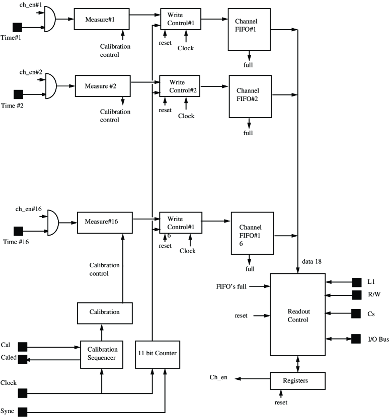
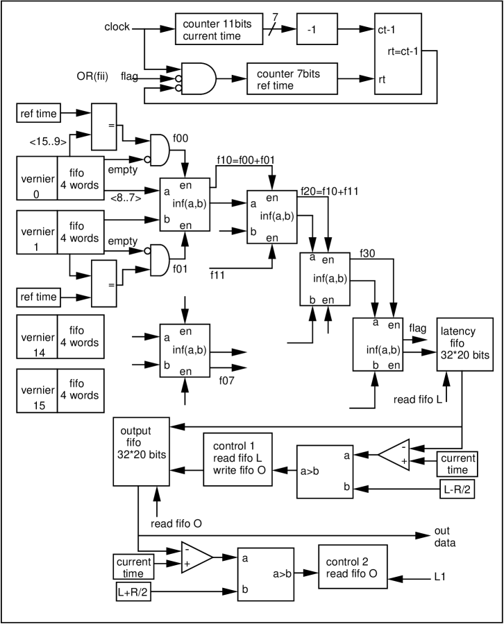
A block diagram of the chip is shown Figure 1. It mostly shows the timing section described in sect. 3.3. The Readout Control box on the figure incorporates the selective readout section (sect. 3.4).
The time measurement proceeds in two steps. On each of the 16 channels, a fine time measurement on 5 bits within a period of the external clock is achieved using voltage-controlled digital delay lines (sect. 3.3.1). The control voltages which synchronize the delay lines on the clock period are provided by an extra identical calibration channel. Thus the delay drifts from temperature, power supplies or the process are compensated by construction. This calibration (sect. 3.3.2) is fully transparent while the TDC is operated. A 11-bit synchronous counter, common to all channels counts the clock ticks to provide the coarse time measurement. In order to allow data-driven operations and asynchronous readout occuring at any trigger time, sixteen dual port FIFOs allow data to be written from the TDC section.
The selective readout uses three levels of buffering in FIFO memories to sort data in time with an incoming trigger, and make them available for readout (sect. 3.4). Each FIFO overload during a trigger window is reported at the end of each data block as a sixteen bit pattern.
3.3 Time measurement
The TDC section integrates one 60 MHz counter, 16 digital delay lines with 32 taps of 500 ps delay each and a calibration channel made of a delay line identical to that of a measuring channel. An incoming signal latches the counter state in a 11-bit register. It is also propagated through the delay line. The next clock positive edge latches the state of the delay line in a 32-bit register, the result being binary encoded to five bits. This method is one of those described in reference[8].
3.3.1 The fine time measurement
The basic cell of a delay line is composed of two CMOS inverters, one of which with its current limited by a voltage controlled resistor (Fig. 2). A complete line is made of 32 cells used for the measurement preceded and followed by 4 cells (underflow and overflow). The control voltage levels are the result of a continuoulsly running calibration process which locks the calibration channel to the external clock. These analog controls are common to all channels, assuming sufficient process uniformity within the chip. The feasibility of the design was known from measurements made on previous TDC chips using the same technology[9].
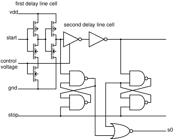
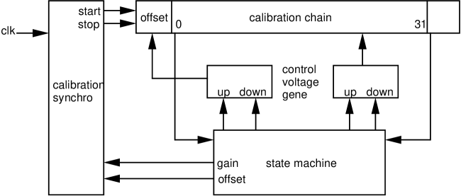
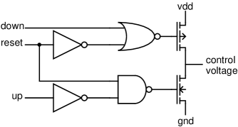
3.3.2 Phase locking
The calibration channel (Fig. 3) coupled with a state machine and two control voltage generators (Fig. 4) tunes two analog voltage levels to lock the total delay of the chain on the external clock period (gain) and to minimize the time offset of the line. The state machine schedules clock pulses to be sent at the calibration channel inputs. In an offset subcycle, a given clock pulse is sent to both the start and stop inputs and the offset control is adjusted until a zero digitization is obtained. Alternately a gain subcycle consists in sending one clock pulse to the start and the subsequent one to the stop. It ends when the fullscale digitization is reached. This process is basically convergent, and no loss of lock has been observed. Therefore, it is not monitored. Calibration is internally activated at 100 , giving the best linearity results.
3.4 Selective Readout
3.4.1 Overview

The block diagram of the selective readout (Fig. 5) shows the 3 levels of buffering implemented using FIFOs. The first level consists of the above mentionned 4 words deep channel FIFOs. They are emptied by a continuous read process at 30 running in the selective readout processor described in the next section (3.4.2). A 32 words deep FIFO called (L standing for latency) shared by all channels, receives the data sorted in chronological order (older first). As soon as the current time reaches that of the earliest trigger the oldest data can stem from, that data is transferred into the output FIFO, . It remains there at most for one trigger resolution. At any given time, thus contains all the data which are compatible with a trigger that could occur then. When indeed an L1 trigger occurs, an automatic readout signal empties and outputs a data packet with a header (containing the L1 time), as many words as present in and a trailer with flags indicating the overloaded channel numbers for that trigger. The readout process is sequenced at 30 . It always terminates before another L1 comes (not before 1.5 s in B A B AR). When data is readout, the process filling is still working. There is no deadtime associated provided the rate remains far from saturation i.e. less than 96 hits (sum of the depths of the FIFOs in series) during one trigger latency.
Detailed simulation studies have been performed to determine the selective readout parameters, namely the depth, the width of the time slices and the characteristics of the comparators used by the fast sort algorithm described next. The test bench results (see 4.3) validate the simulation for the rates specified in the requirements for which the time to move the data in the FIFOs contributes very little.
3.4.2 Fast sort
A dichotomic algorithm pictured on Fig. 6 selects the oldest data in the channel FIFOs during 256 time windows using 2-bit comparators. The comparisons have a 64 precision and the result of one round is available after 18 . They are performed on time slices delayed at least by one slice width with respect to the current time (given by the synchronous counter) to avoid carry problems (when the counter wraps around). The width of 256 is fixed by the response time of the comparator tree, and the required maximum input occupancy.
3.5 Fault simulation
A scan path has been implemented. The Built-In Self Test generator of the Silicon manufacturer has also been used for their FIFOs. 18k test vectors have been used, some of which were written by hand, for a fault coverage of 90 of the chip.
3.6 Layout
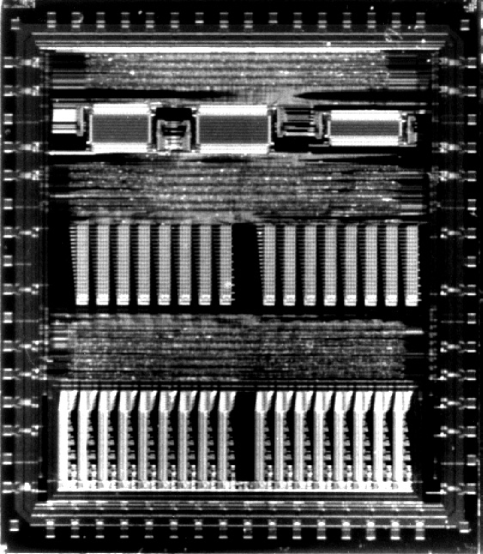
The layout (Fig. 7) has been done using the most appropriate style regarding the functionality.
TDC section and channel FIFOs (full custom). A stick layout symbolic editor[13], into which the silicon manufacturer’s design rules were input, was used to draw the sections critical for timing or silicon area: the delay chains, the fast counter, the charge pump and associated controls, the synchronization logic. All analog sections have been simulated with HSPICE before and after layout. Sufficient margins were used to ensure the required behaviour in a temperature range of 20 15 ∘C with a 10% voltage supply variations. A compact layout is obtained for the full custom part which occupies about half the chip area.
Latency and Output FIFOs. The latency and output FIFOs have been generated using the automated tool of the Silicon manufacturer as blackboxes to be filled when making the masks. Test vectors have also been generated automatically. A model for these FIFOs has been written in the Verilog hardware description language from which the associated counters and glue logics were merged into the the standard cells generated by the compiler Synergy. In this case as well, a post-layout simulation has checked the design accommodated temperature, voltage supply and process variations within the safety margins recommended by the manufacturer.
Random logic. The random logic has been implemented as standard cells, using the library of the manufacturer. A Verilog model was also provided.
Verilog models of the TDC sections have been written to simulate the chip globally. The full die size is 36 mm2.
4 Performance tests
The test bench described in section 4.1 was used to study the integral and differential linearities of the timing measurements (sect. 4.2) and the selective readout performance (sect. 4.3). The locking frequency range of the calibration (from 45 to 90 ), the cross talk between channels (none was found) and the sensitivity to the environment were also studied with the bench. The temperature coefficient is estimated to be 2.5 per ∘C and the supply voltage coefficient to be 500 per V. The manufacturer was given an array of 18k test vectors to check the digital functionality of the chip. Only chips which passed that test were delivered (1250 parts). Of those 97 % matched the specifications. A further selection was finally done to sift the best 805 chips (672 parts plus spares) for the DIRC. Further tests of the TDC were performed on the DFBs as part of the global commissionning of the DIRC electronics. At present the BABAR experiment including the DIRC is taking cosmic ray data and the TDCs as part of the DIRC system perform satisfactorily.
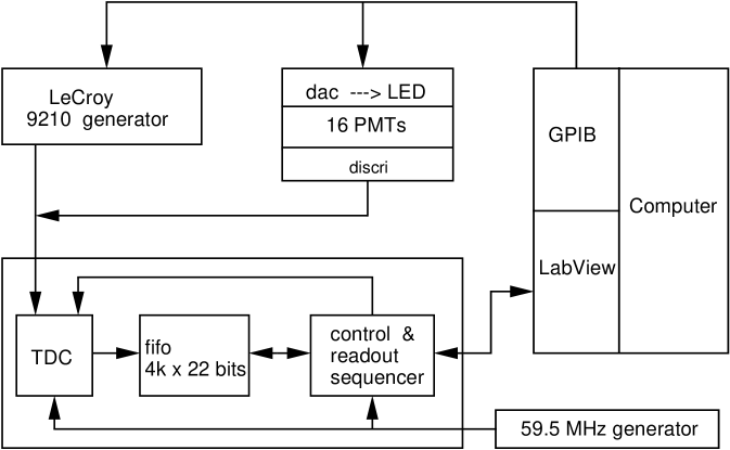
4.1 Test bench
Fig. 8 pictures the test bench. It uses 16 phototubes that can be illuminated by an LED the light output of which is adjustable to vary the rates. The TDC channels can be fired either by the discriminated pulses from the PMTs or by precisely timed signals from a pulse generator (LeCroy 9210). The time base (59.5 external clock) is produced by another precision pulser. A custom made four layer printed circuit board with the TDC, a 4k 22-bit word FIFO and a fast readout sequencer, is interfaced to a computer running LabView.
4.2 Time measurement
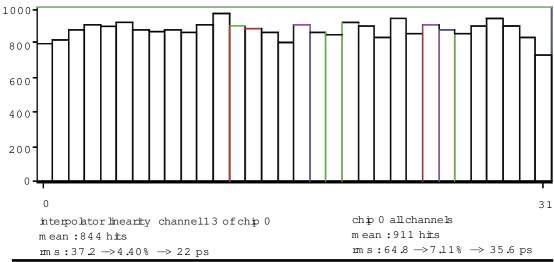
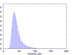
The linearity of the time measurement was tested locally and globally. For the differential linearity both random and deterministic methods were used. In the latter the delay between start and stop is varied in 10 steps across one delay line range (from 0 to 16 ). The measured time plotted against the set time showed the expected step curve. The difference between the measured and the set times had a standard deviation close to the expected 0.29 lsb111least significant bit. (lsb/) and never worse than 0.73 lsb or 383 , a figure well within the specifications. In the random method, the TDC channels are fired at an average rate above 100 from PMTs at random times with respect to the clock and the linearity is inferred from the deviation from uniformity of the distribution of the 5 least significant bits of the measured times. A typical result is shown Fig. 9. Worse results where the last bin is up to two times too wide were obtained for the edge channels of some chips, in particular those numbered 14 and 15. This unexpected non linearity is presumably a layout residual effect.
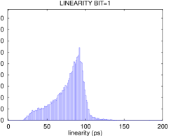
The local measurements could only test the fine time measurement. To prove that the fine and coarse scales matched seamlessly a global procedure was devised. The generator is run at 500 and asynchronously from the trigger to produce double pulses with a time spacing of 15 clock periods plus 520 (that brings the measured difference at the limit between 32 and 33 lsb). The measured time difference is recorded for 12000 triggers, enough to test the transition for 90 % of the synchronous counter codes. A few occurrences of a mismatch between the coarse and fine time measurements were found in those and further tests (performed on the DFB frontend boards). 3% of the channels were anomalous when the input rate was 30 times the rate specified in the requirements. Careful analysis revealed that the affected channels were edge channels with too wide a bin 31. It so turns out that the two problems, the existence of too wide bins for the edge channels and the occasional slipping of the synchronous counter, are correlated. The parade is to phase lock only 31 bins of the delay lines (instead of 32) to the external clock. Doing so, slightly worse results are obtained for the linearity (the average is 73 ). However, they correspond to timing resolutions (196 on average) well within specifications. And, most importantly, the probability of a carry problem becomes negligible for the specified input rates. The differential linearity statistics obtained with the random method in the two cases are displayed on Figure. 10.
4.3 Selective readout
The selective readout process has been checked by sending on an input a (500 ) signal one latency before the trigger while the other 15 received random PMT pulses at a rate up to 2 . No loss of data is observed. The signal is observed on its input channel while the others exhibit the expected accidental rate. The histogram of the time difference between the trigger and the recorded time measurement shows a peak at the expected value above a flat distribution again compatible with the accidental level (see Fig. 11) with the expected width corresponding to the trigger resolution setting and the fast sort algorithm properties.

The system detecting the channels with overloaded input has been tested satisfactorily.
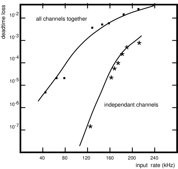
An experimental determination of the dead time loss is obtained from the ratio of the rate of all overloaded channels to the rate of good time measurements. A comparison to the simulated computation (Fig. 12) shows a good agreement for the two extreme cases that were studied: the case where all inputs receive independent random pulses at the specified rate and the case where all inputs are simultaneously fired by one and the same random input pulse at the specified rate.
5 Conclusion
The digital TDC chip described in this paper is a major building block of the DIRC frontend electronics since it captures the PMT hits and selects those in time with the trigger. The time is measured from an external reference clock with a typical frequency of 60 with a 0.5 lsb over a range of 32 . The data driven architecture enables to eliminate background data as soon as possible on the frontend without resorting to pipelines. It is a mixed analog and digital IC which was produced at ATMEL-ES2 using a 0.7 CMOS process with an excellent yield (97%). The 1213 good parts have performances above the specifications. The DIRC detector equipped with them is presently taking cosmic ray data at SLAC. The time distribution of cosmic ray tracks (Fig. 13) is conform to expectations.

Acknowledgements
This work has been supported by Institut National de Physique Nucléaire et de Physique des Particules, IN2P3 from the Centre National de la Recherche Scientifique, CNRS (France). It benefited a lot from discussions and collaborative work within the BaBar and DIRC Electronics communities as well as within LPNHE. One of the authors has been supported by the government of China while at LPNHE Paris as a foreign visitor.
References
- [1] “B A B AR Technical Design Report”, D. Boutigny et al., SLAC-R-95-457 (1995).
- [2] “An Asymmetric B Factory based on PEP: Conceptual Design Report”, edited by M. Zisman, SLAC-372, LBL PUB-5303 (1991).
- [3] “The B A B AR Physics Book, Physics at an Asymmetric B Factory”, P. F. Harrison and H. R. Quinn Editors, SLAC-R-504 (1998).
- [4] http://www.slac.stanford.edu/BFROOT/doc/DIRC/
- [5] “Systematic tests of DIRC phototubes”, Ph. Bourgeois et al., B A B AR DIRC Internal Note #105 (1998).
- [6] “Test of a Large Scale Prototype of the DIRC, a Cherenkov Imaging Detector based on Total Internal Reflection for BaBar at PEPII”, H. Staengle et al. Nucl. Instrum. Methods A, 397 (1997) 261.
- [7] “Développement d’un circuit intégré VLSI assurant mesure de temps et lecture sélective dans l’électronique frontale du détecteur DIRC de l’expérience B A B AR à SLAC”, B. Zhang, Thèse de Doctorat, Université Pierre et Marie Curie Paris, France (Sept. 1997).
- [8] “High Resolution Time to Digital Converters”, J.F. Genat Nucl. Instrum. Methods A, 315 (1992) 411.
- [9] “A 100 resolution time to digital converter chip in CMOS technology”, P. Bailly, J.F. Genat in Proc. of the Int. Conf. on Electronics for High Energy and Nuclear Physics, LeCroy, New-York (May 1993), talk given by J.F. Genat.
- [10] “A 500 picosecond resolution TDC for the DIRC at BaBar”, P. Bailly, J. Chauveau, J.F. Genat, H. Lebbolo, B. Zhang, in Proc. of the Int. Conf. on Electronics for High Energy and Nuclear Physics, LeCroy, New-York (May 1997), talk given by H. Lebbolo.
- [11] “The BaBar DIRC Front-end Electronics”, P. Bailly et al., in Proc. of the 1998 IEEE Nuclear Science Symposium, Toronto, Canada (1998).
- [12] “A Discriminator and Shaper Integrated Circuit.”, J. Ardelean, R. L. Chase, A. Hrisoho, S. Sen, V. Tocut, K. Truong, G. Wormser, in Proc. of the 1998 IEEE Nuclear Science Symposium, Toronto, Canada (1998), talk given by A. Hrisoho.
- [13] “PREFORME : Manuel d’Utilisation”, J.F. Navinier and J.C. Dufourd, Ecole Nationale Supérieure des Télécommunications (ENST), Paris (1993) unpublished.