TDC Chip and Readout Driver Developments
for COMPASS
and LHC-Experiments
Abstract
A new TDC-chip is under development for the COMPASS experiment at CERN. The ASIC, which exploits the CMOS sea-of-gate technology, will allow high resolution time measurements with digitization of , and an unprecedented degree of flexibility accompanied by high rate capability and low power consumption. Preliminary specifications of this new TDC chip are presented.
Furthermore a FPGA based readout-driver and buffer-module as an interface between the front-end of the COMPASS detector systems and an optical S-LINK is in development. The same module serves also as remote fan-out for the COMPASS trigger distribution and time synchronization system. This readout-driver monitors the trigger and data flow to and from front-ends. In addition, a specific data buffer structure and sophisticated data flow control is used to pursue local pre-event building. At start-up the module controls all necessary front-end initializations.
1 Introduction
The COMPASS experiment at CERN will investigate hadron structure by deep inelastic scattering processes and in addition pursue different aspects of hadron spectroscopy using hadron beams. Comparison with calculations based on operator product expansion or lattice techniques and with model predictions based on chiral symmetry or effective degrees of freedom will help to improve our understanding of hadrons. To reach this objective a new state-of-the-art fixed target spectrometer, capable of standing beam intensities of up to particles/spill and with excellent particle identification, will be put into commission in the year 2000.
These challenging physics goals of the COMPASS Experiment can only be met, if at highest possible beam rates large data statistics can be recorded. This leads to the requirement of an experiment with negligible dead time, which can digest data rates of several Gigabyte per second. This is at the edge of today’s digitization and bandwidth technologies.
The initial approach of the experiment was to minimize dead time by reading digitized data through pipelines where applicable. Availability of and resolution requirements on digitization units have made this goal not feasible for every detector component. The present scenario assumes a maximum dead time of 500 ns for analog sensitive front-end electronics which will digitize signal amplitude or charge with a precision better than 10 bit.
The readout architecture of the COMPASS experiment is summarized in Figure 1. Data are digitized right at the detector by the front-end electronics wherever possible. In case of analog readout the pedestal subtraction and zero suppression is performed by the front-end at the detector. To suppress background for time measurements only those hits are transfered to the data recording units which have a correlation to a trigger time.
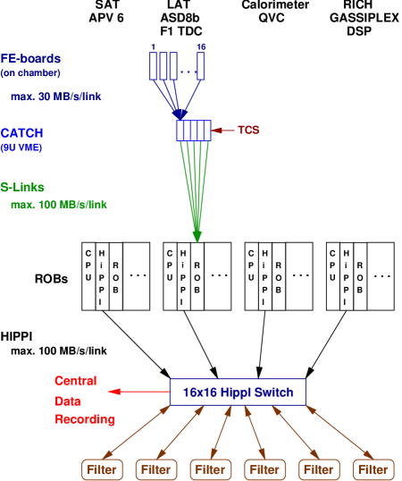
The data are transmitted from the front-end to CATCH modules (CATCH = COMPASS Accumulate, Transfer and Cache Hardware). The functionality of the CATCH will be described below.
From the CATCH data are transmitted via a standardized link to the read-out buffers (ROB) which can store all data from one spill. The backbone of this data transfer is the S-link [1] interface and the S-LINK data transfer protocol. Presently about 128 S-LINK connections are foreseen to transmit data with a maximum total bandwidth of about 12 GB/s.
The read-out buffers combine data which belong to one event, check consistency of the data and perform sub-event-building. In a next step they transmit the sub-events via HiPPI [2] or Gigabit Ethernet to filter computers. Here the final event-building is performed and events are reconstructed. The filter farm will reduce the data based on physics cuts by a factor of 5 to 10 and a continuous rate of 12 to 24 MB/s will be transfered to the central data recording facilities at CERN.
2 The TDC Chip
A key element in the experiment is a new developed dead time free TDC chip, the . It will be used to digitize the data from a large majority of detectors. Table 1 shows that the required specifications vary significantly for the foreseen applications of the chip. Certainly the most challenging demands are defined by the scintillating fiber (SCIFI) detectors. Count rates up to 6 MHz per channel and time resolution better than 100 ps are on the edge of today’s technology. When count rates and background become too high, existing limitations in bandwidth on data-links between TDC and the data recording system require on-chip event selection. Detector components like Plastic Iarocci Tubes (-Detector 1) or MWPC do not ask for precise timing but require lowest cost/channel due to the large number of channels involved. Thus multiplexed input is desirable for this kind of detectors. We were forced to develop a new multi-purpose TDC Chip, because no integrated TDC circuit is currently on the market with a sufficient degree of integration and flexibility to fulfill all requirements of COMPASS. In spite of the short time available for the R&D phase for COMPASS we decided to develop a TDC in collaboration with acam [3], a recently founded German enterprise specialized in the development of time measurement devices and applications.
| detector | channels | time | background | event |
|---|---|---|---|---|
| resolution | rate | rate | ||
| ps | kHz | kHz | ||
| Straws | 37000 | 1000 | 600 | 100 |
| Mega Chambers | 15000 | 500 | 100 | 100 |
| -Detector 1 | 9000 | — | 50 | 1 |
| -Detector 2 | 3000 | 2000 | 130 | 1 |
| MWPC | 18000 | — | 600 | 100 |
| SCIFI | 1280 | 320 | 600 | 6000 |
| Beam Scintillators | 512 | 100 | 600 | 6000 |
| Recoil-Detector | 5000 | 100 | 100 | 100 |
| Hodoscope | 1200 | 100 | 100 | 100 |
The development of the resulted in a highly programmable eight channel TDC ASIC based on a low cost m CMOS sea-of-gates process. The reasons for only eight channels in a single chip are driven by financial considerations as well as physical limitations. Eight channels in a chip optimize savings due to density on the die and costs for bonding and chip package. In addition chip prizes depend strongly on the number of produced chips and less on the die surface. Hence 6000 chips with 8 channels are more cost efficient than 1500 chips with 32 channels.
The scheme utilized in the avoids the use of high-speed clocks and shift registers and, therefore, results in very low power consumption. Signal propagation times in gate arrays have very large variations as a function of temperature and operation voltage. Furthermore signal propagation within gates have a spread strongly dependent on the production process. To overcome these disadvantages the exploits a self calibrating method utilized by voltage controlled delay elements as part of an asymmetric oscillator in a phase locked loop (PLL).
An outline of the chip is shown in Fig. 2. Non-perspective displayed boxes - like trigger counter, PLL or interface FIFO - refer to units which are shared between the eight channels, whereas the perspective displayed boxes - like hit buffer, trigger matching and readout buffer - indicate logic units in the chip which come eightfold and are not shared between the channels.
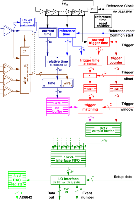
The preliminary specifications for the TDC are listed in Table 2. The can be considered as a real multi-purpose chip with very different modes of operation in terms of resolution and functionality.
| Number of channels: |
| 4 for high resolution mode |
| 8 for standard resolution mode |
| 32 for pattern recognition mode |
| Time bin size: |
| 75 ps for high resolution mode |
| 150 ps for standard operation mode |
| 5700 ps for pattern recognition mode |
| Reference-clock frequency: |
| Between 500 kHz and 40 MHz |
| (Clock is used for self calibration only) |
| Differential non-linearity: |
| Less than 0.05 LSB for high resolution mode |
| Less than 0.2 LSB for standard mode |
| Integral non-linearity: |
| Less than one time bin |
| Variation with temperature: |
| Less than one time bin |
| Dynamic range: |
| 16 bits |
| Double pulse resolution: |
| Typical 22 ns |
| Digitization and readout dead time: |
| None |
| Hit buffer size: |
| 32 measurements for high resolution mode |
| 16 measurements for standard mode |
| 16 measurements for pattern recognition mode |
| Output buffer size: |
| 8 measurements |
| Readout Interface: |
| 16 measurements |
| Trigger buffer size: |
| 4 |
| Power Supply: |
| 5.0 V, optional 3.3 V with reduced resolution |
| 30 mA - 80 mA, depending on trigger load |
| Temperature range: |
| -40 to +85 degree centigrade |
| Hit input: |
| LVDS or TTL |
| Package: |
| 160 PQFP |
In the standard mode the is an eight channel TDC chip with a digitization uncertainty of 150 ps. When a leading or trailing edge of a LVDS-signal [4] is present at one of the channel inputs the time relative to the last reset of the TDC is derived from a PLL and a coarse counter. The time stamp is written into the hit buffer. When a TTL signal edge is present at the trigger input the time relative to the last reset is measured for the trigger signal. In a next step the time stamps, which are stored in the hit buffer, are compared to the time stamp of the trigger time. Data within a pre-set time window are accepted for readout and copied to the output buffer. An 8 or alternatively 24 bit parallel bus is used for readout of the chip. The data bus can be operated at a maximum frequency of 50 MHz.
In the high resolution mode two channels are interleaved by 1/2 least significant bit (LSB) delay. Hence in this mode the has four channels with a resolution of 75 ps and the hit buffer for a single channel is increased by a factor of two. Otherwise the principle of operation is the same as in the standard mode.
The third way to operate the chip is the pattern recognition or latch mode. In this mode 32 input channels are connected to eight groups of fourfold latch-registers. Once a leading edge of a signal is detected on a input channel the fourfold input register is activated for the duration of a pre-set time interval and subsequent hits on the other inputs can be registered as well. When the pre-set time has passed, the register is copied to the hit buffer and cleared for new recording. While this transfer is realized a time-stamp with reduced resolution is taken and added to the information from the register.
In the fourth mode the chip can be used like any other normal common-start TDC. After a start-signal on a dedicated start-input has been applied all subsequent time measurements are relative to this start-signal. In this mode the time-stamps are immediately passed to the output bus and not stored in the hit buffer. This mode does not make use of the trigger-matching possibilities of the TDC.
Initialization of the -chip is performed via a 10 Mbps serial connection. The interface for this link is integrated in the TDC chip and no additional external control is needed.
As an additional feature the has eight eight-bit registers and a dedicated interface to an eight channel digital-to-analog converter (AD8842) [5], which can be used for threshold control of discriminator units placed on the front-end cards. The integration of the register and the interface in the TDC avoids additional memory and controller units on the front-end board.
3 Readout Driver Boards for COMPASS
The basic philosophy behind the COMPASS readout architecture design was to unify as much hardware components as possible to save on spare parts and manpower during preparation and during the data-taking phase of the experiment. Having this concept in mind we decided to concentrate the data as close as possible to the front-end into few high-bandwidth data streams. A logic consequence was the development of a standardized data multiplexer board, the CATCH, for all the different components of the COMPASS detector. The CATCH functions mainly as a derandomizer and must provide enough memory for intermediate storage of several events. To concentrate a large number of channels we decided to build the CATCH as a 9U VME board. However, the VME bus will only be used for power distribution, for transfer of set-up data during detector initialization and to spy on a sub-sample of events parasitically - but independent of the data acquisition system - during data taking.
Data input to the CATCH can be performed in several ways. The data-interfaces to the CATCH are designed as mezzanine cards following the IEEE CMC standard [6]. The advantage of mezzanine cards is that they allow easy and fast exchange without hardware modifications and thus give the highest degree of flexibility. Currently we design four different types of mezzanine cards: One card contains four 30 MByte/s HOTLink de-serializer receiver-chips [7] which will be used for front-end boards mounted on the detector; a second card contains -chips to assemble TDC boards; a third mezzanine card which contains several FPGA to implement fast 200 MHz dead-time-free scalers and a fourth card which will serve as an interface to the silicon detector readout boards.
The output of the CATCH module is connected through the P2 connector to a S-LINK multiplexer board mounted on the backplane of the VME crate. This multiplexer board is used to optimize the transmission rate on the S-LINK to the available S-LINK bandwidth, which is 100 MB/s/link. Figure 3 illustrates, as an example for the data flow on the CATCH, the use of the Cypress HOTLink receiver-chip as data input source. In this example 24 bit data words are transmitted in three words of one byte each.
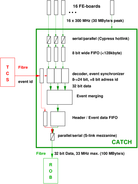
The data interfaces are scanned continuously for arriving events. All data are reformatted to 32-bit words and, if necessary, additional hardware addresses are added. These are transfered by the front-end only during the initialization process for unambiguous identification. Next all data from a trigger are packed between a S-LINK header and S-LINK trailer. The S-LINK header and trailer contain a unique bit pattern for identification. Furthermore a S-LINK header contains an event- and spill-number and describes the data source and event type. For each individual event the information contained in the header is received by the CATCH from the Trigger Control System (TCS). The data for one event are passed to the ROB when all front-end cards, which are connected to a CATCH, have transmitted either valid-data or an empty-data word for a particular trigger-number.
The CATCH module can also be used to erase data based on second level decisions from the readout stream. To implement this feature in an experiment the trigger numbers of events, which are rejected by the higher trigger level, have to be distributed to the CATCH boards via the trigger control system. The latency of the second level trigger decision and the total data rate per CATCH determines the memory needed to store events before they are passed to the ROB. Currently the implementation of several data compression methods on the level of the CATCH modules are discussed as a possibility for further reduction of data rates.
The handling of trigger signals from TCS on the CATCH board is illustrated in Figure 4. The CATCH-module receives trigger signals and a reference clock from the TCS via optical data transmission. The TCS interface board contains an optical or copper cable receiver and a unit to decode the time-division multiplexed signals transmitted by the TCS. The TCS receiver board can be mounted to the P2 connector on the backplane of VME crates. Once the CATCH receives a trigger signal from the TCS it encodes the signal as a pulse with the length of one clock cycle. The encoded trigger signal is passed immediately to the front-end cards synchronous to the COMPASS reference clock (38.88 MHz). To check data for consistency a local event number is generated and compared to the event numbers transfered with the data headers from the front-end.
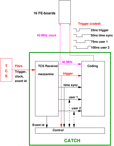
The physical network layer between front-end and CATCH is realized in standard S/STP CAT 6 [8] cable. This cable is widely used in Ethernet links between wall outlets and personal computers. The great demand for this kind of cable makes it the cheapest solution to connect two points with four differential lines up to frequencies of 700 MHz. In our application one differential line is used to distribute the COMPASS 38.88 MHz reference clock to the front-end. The second line is used to distribute up to four different user signals to the front-end. The signals are distinguished by their length with respect to the COMPASS reference clock. One of the four possible signals is the trigger-signal and another is a time synchronization reset at the beginning of a spill. The remaining two can be defined according to user requirements. A third line is used for as serial link to down-load initialization data to the front-end electronics at start-up. This serial line is operated at 10 Mbps. The fourth line is used to transfer the serialized data from the HOTLink transmitter (front-end) to the HOTLink receiver (CATCH).
4 Acknowledgement
This work would be impossible without the significant efforts by the staffs of the collaborating institutions, in particular those involved in front-end electronics development. The developments described in this report are supported by the German Bundesministerium für Bildung, Wissenschaft, Forschung und Technologie.
References
- [1] E. van der Bij et al., S-LINK: A Prototype of the ATLAS Read-out Link, Fourth Workshop on Electronics for LHC-Experiments, Rome, September 21-25 1998.
- [2] ANSI X3T9.3/91-005, High Performance Parallel Interface Standard.
- [3] Address: acam-messelectronic gmbh, Haid-und-Neu Str. 7, D-76131 Karlsruhe; EMAIL: support@acam.de.
- [4] IEEE P1596.3-1995, Draft Standard for Low-Voltage Differential Signals for Scalable Coherent Interface.
- [5] Analog Devices, Norwood, MA 02062-9106 Datasheet: AD8842, an 8-Bit Octal CMOS TrimDAC.
- [6] IEEE P1386, Standard for a Common Mezzanine Card Family: CMC.
- [7] Cypress Semiconductor, CY7B923/CY7B933 HOTLink Transmitter/Receiver Preliminary data Sheet, Cypress Semiconductor High Performance Data Book, August 1, 1993.
- [8] ISO/IEC 11801:1995 Information technology – Generic Cabling for Customer Premises.