The Charge Collection Properties of CVD Diamond
Abstract
The charge collection properties of CVD diamond have been investigated with ionising radiation. In this study two CVD diamond samples, prepared with electrical contacts have been used as solid state ionisation chambers. The diamonds have been studied with beta particles and 10 keV photons, providing a homogeneous ionisation density and with protons and alpha particles which are absorbed in a thin surface layer. For the latter case a strong decrease of the signal as function of time is observed, which is attributed to polarisation effects inside the diamond. Spatially resolved measurements with protons show a large variation of the charge collection efficiency, whereas for photons and minimum ionising particles the response is much more uniform and in the order of 18%. These results indicate that the applicability of CVD diamond as a position sensitive particle detector depends on the ionisation type and appears to be promising for homogeneous ionisation densities as provided by relativistic charged particles.
keywords:
CVD Diamond, Charge Collection Efficiency.PACS:
29.40, , , , and ††thanks: Corresponding author, e-mail: Alexander.Oh@desy.de.
1 Introduction
In recent years, diamond as a possible material for particle detectors has been the subject of considerable interest [1, 2, 3]. Significant progress in the techniques to produce synthetical diamond films of very high quality has been achieved by means of the Chemical Vapour Deposition method (CVD). A number of commercial manufactures of CVD diamond films [4, 5] and research institutes [6] have made systematic studies of the properties of this material feasible. The main advantage of the material compared to other semiconductor detector materials is its radiation hardness, which has recently been demonstrated to neutron fluences of up to [7]. The radiation hardness of the material is of strong interest for the detector development at projected experiments where high radiation levels are expected due to the increasing luminosity and energy, as e.g. the experiments at the Large Hadron Collider at CERN. The main problem of using CVD diamond as a detector material are the charge collection properties, since an application as a detector for ionising particles requires that the material response is homogeneous throughout the volume and that a sufficient fraction of the produced charge is collected. General studies of the CVD diamond growth conditions for detector applications with a large sample are presented in [6].
In this paper we present different studies of the charge collection properties of CVD diamond films. We investigate both the bulk properties of the material and the behaviour of charge produced close to the surface.
1.1 Principle
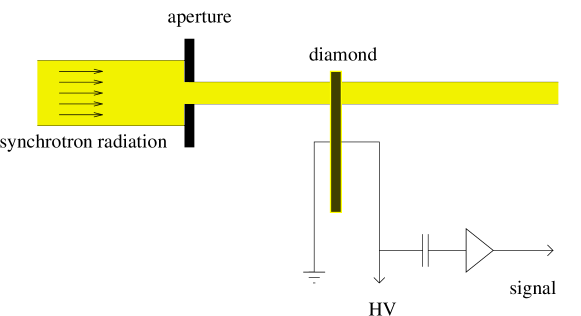
One of the aspects which make CVD diamond films an attractive material for the detector development is its very high specific resistivity of . This allows a very simple construction of a detector as a solid state ionisation chamber (see fig. 1). By contacting the material on opposite sides and applying a sufficient potential across the contacts, charges produced in the bulk of the material by an incident charged particle start to drift towards the electrodes

and induce mirror charges. The ratio of the amount of charge measured, , to the amount of charge produced, , is the collection efficiency
The efficiency is below 100%, if trap- or recombination-sites in the material hinder the charge carriers to reach the electrodes, as is the case for diamond. The mean free path length , also called Schubweg [8], for each type of charge carriers ( for electrons and holes) can be expressed as the product of the mobility , the electric field strength and the life-time , as
The combined mean free paths of electrons and holes,
| (1) |
is the mean distance a hole and an electron can separate. This distance is referred to as the collection distance [1]. The collection distance and the efficiency are related according to Ramo’s theorem [9] by
| (2) |
with being the detector thickness.
The above discussion holds for uniform ionisation within the detector volume and . If the charge is created in the vicinity of one electrode (, with the distance of the charge to the electrode) the van Hecht-equation [10] relates and as
| (3) |
where denotes the Schubweg for electrons
and holes respectively, depen-
ding on the direction of the
electrical field.
Throughout this paper, we will use the quantity because the definition of involves fewer assumptions than the charge collection distance. However, the values are given in collection distance as well where appropriate.
Systematic studies of the dependence of on growth parameters have shown that high values of are reached for films produced with slow growth rates [6]. Until now charge collection efficiencies of up to 38% [6] have been reported.
It is known that the exposure of diamond to ionising radiation and UV-light can substantially increase . This phenomenon is called priming [11]. The passivation of traps by occupation with free charge carriers is the reason for the observed behaviour. The same mechanism leads to a deterioriation of the signal as for example seen when irradiating diamond with alpha particles or protons at energies corresponding to stopping ranges of a few micron. The deterioriation is caused by the build-up of space charge and the resulting compensation of the applied field [12].
Another important issue is the homogeneity of . It is known that the collection distance (which relates to by eq. 2) varies with the film thickness, as low values are typically observed on the substrate side and high values on the growth side. This is due to the fact that polycrystalline CVD diamond films consist of several columnar micro-crystallites. Typically the crystallites are very small at the beginning of the growth process and become larger as the film thickness increases [13]. A linear model has been proposed to describe the collection distance as a function of the film thickness [14]. For an application as a particle detector, it is important that the average is constant over the active detector area. While highly energetic minimum ionising particles yield a rather homogeneous response (see section 3), it has been shown that this is not the case for particles depositing their charge in a thin surface layer [12, 15]. Thin films for which the stopping range of the ionising particle is of the order of the film thickness seem to exhibit a more homogeneous response [16].
1.2 Methods of investigation
We investigate the charge collection properties of CVD diamonds by four different methods. The response of CVD diamond to homogeneous ionisation densities has been measured with beta particles from a source. The ionisation density produced by beta particles above is similar to the ionisation density produced by minimum ionising particles (MIPs), which are to be detected in the application as a vertex detector in a high energy particle physics experiment. By fitting the pulse height distribution, we obtained information about the homogeneity of . To investigate the priming effect on the CVD diamond samples, has been measured with beta particles while the samples were under continuous exposure of ionising radiation. In a second experiment, the diamond has been scanned with a beam of 10 keV photons. The photons ionise via the photo effect and produce when averaged over many events a similar ionisation density distribution as MIPs. With this method the local variations of have been measured with a resolution of about . The results are compared with the data obtained with MIPs.
In contrast, the other two methods described in this paper use radiation which produces charge carriers only in a shallow layer below the surface. Hence, these methods are not measurements of the bulk properties as are the first two. Since all the produced charge is deposited in a surface layer of the detector, they are more sensitive to polarisation effects, as will be discussed in section 7. One method uses alpha particles from an source. Various pulse height spectra have been recorded at different electrical field strengths and polarities in order to extract information about . The other method uses protons with an energy of 2 MeV and allows to do a spatially resolved measurement. The recorded pulse spectra are mapped onto the diamond surface. The spatial information has been used to compare the data to SEM (scanning-electron-microscopy) pictures and to data obtained with the 10 keV photon beam described above.
2 Sample preparation
For the studies presented here, two CVD diamond samples produced by different manufacturers (sample A from Norton [17] and sample B from FhG [18]) have been used. The sample A was initially grown to a thickness of after which were removed from the substrate side [4]. The growth side has been polished to reduce the surface roughness, which has been measured to be smaller than after polishing [4]. The grain-size on the growth side is in the order of . No information is available about the grain size on the substrate side. The sample size is . Sample B has been grown to a thickness of and is not polished. The grains have a typical size of on the growth side. From SEM we estimate a surface roughness of below . The sample has a circular shape and a diameter of . Pole figure measurements [19] showed no preferred orientation for sample A and a slight (111)-texture for sample B.
In order to provide electrical contacts, both samples have been metallised on growth and substrate side with layers of Ti (50 nm), Pt (30 nm) and Au (60 nm), followed by an annealing step and treatment in oxygen plasma to reduce surface conductivity [20]. The quality of the contacts has been checked by measuring the current-voltage (I-V) characteristic in darkness at room temperature. All I-V-curves are symmetric, i.e. independent of polarity, indicating, that front and back-contact are of the same type. The specific resistivities and some of the properties of the samples are listed in table 1.
| Producer | Name | Process | [ ] | ||
|---|---|---|---|---|---|
| Norton | A | DCAJ | no information | 300 | |
| FhG | B | MWP | 1.3 | 123 |
3 Measurements with beta particles
The average charge collection properties of the diamond samples have been investigated using beta particles. Since they traverse the detectors, they probe along the particle trajectory, and result in a measurement averaged over the detector thickness. This method is widely used to characterise diamond samples, since it corresponds most closely to the situation of a real detector application.
The field dependence of has been measured for the two samples. From the shape of the distribution of the collected charge we have obtained information about the variation of laterally.
The dependence of on the absorbed radiation dose of the samples has also been studied. The priming effect of ionising radiation has been established, and for each sample the characteristic priming dose constant has been derived.
3.1 Experimental set-up
Beta particles have been used emitted from a source () which have a maximum energy of 2.28 MeV to measure averaged over the bulk of the material. A diagram of the experimental set-up is shown in figure 2. The beta particles were collimated by a aperture in a Plexiglas block. The diamond was placed in the collimated beam of beta particles followed by a silicon detector which was used as a trigger device.

The aperture ensured that all beta particles traversed the sensitive region of the diamond-detector. After having traversed the diamond, the beta particles had to deposit enough energy () in the silicon-detector to be accepted as an event. The trigger-rate was limited by the DAQ system to about 15 Hz. The characteristic energy-loss of the beta particles in the diamond is approximately that of minimum ionising particles (MIPs) which on average produces electron-hole-pairs in diamond [1]. The collection efficiency is given by
where is the diamond thickness in and the average image charge induced on the electrodes of the diamond detector.
The charge was measured with a charge-integrating amplifier Amptek A250 followed by a shaping-amplifier Ortec 572 with a shaping-time constant of . The signal was read out with a digital scope and averaged over 3000 events to improve the signal-to-noise ratio. Additionally, the signal was recorded with a multi channel analyser (MCA).
In a second experiment the sample was alternately exposed to a strong source () without applying a voltage and to the weaker source described above to measure . With this set-up the dose dependence of was measured.
3.2 Experimental results


The charge collection efficiency as a function of the field strength (fig. 3) exhibits a sharp rise with up to about 1 kV/cm for both samples. At higher field strengths, the curve flattens due to enhanced phonon creation and the resulting decrease of the mobility [1]. Above an applied voltage of , the signal became noisy for both samples, because the leakage current increased. As the corresponding field strengths differ by a factor this is taken as indication for surface currents.
When the samples were irradiated, a dose-dependent increase of was observed. In fig. 4, the dose-dependent development of for three different field strengths is shown. The initial drop of on sample B is suspected to be due to polarisation effects. The same behaviour has been observed for sample A at 4.3 kV/cm and 3.3 kV/cm. We have fitted a function of the form
| (4) |
to the monotonically rising part of the data and extracted the priming-dose constant .
The unprimed and primed efficiencies, the ratio of unprimed over primed efficiency, and for the two samples are summarised in tab. 2. The ratio of in the primed to the unprimed state is compatible for the two samples, whereas is significantly different.


| name | , unprimed | , primed | [rad] | ratio |
|---|---|---|---|---|
| A | ||||
| B |
The primed state of the diamonds has been observed to be stable for days. The diamonds can be reset to the unprimed state by illumination with light in the visible region. IR-light was found to have no effect on the primed state. UV-light with a spectrum extending to about 5 eV did not show this reset effect but instead a priming effect on the diamonds.
A pulse-spectrum of sample A in the primed state is shown in fig. 5. By fitting the spectrum with a function, which is based upon the theoretically expected shape and allows for a Gaussian distribution of , information about the width of can be obtained.
A description for the pulse spectrum of MIPs in thin detectors is the Landau distribution, which does not place a limit on the maximum energy transfer and thus is only a rough approximation for beta particles with a maximum energy of as used in this experiment. A more general description was derived by Vavilov [21], taking into account the particle velocity, , and the ratio of the mean energy loss of the particle in the target and the maximum allowed energy transfer in a single collision with an atomic electron. To fit the pulse spectrum, we used an implementation of this more accurate Vavilov distribution [22], , where is a scaling parameter and is an offset parameter. To account for electronic noise and possible intrinsic variations of , the Vavilov distribution has been folded with a Gaussian, , with a width . The complete fit function is given by
| (5) |
with being a normalisation factor. For the fit, we used , and . The values are motivated by the assumption that the average energy of the beta particles contributing to the spectrum was . The maximum energy transfer was taken to since an energy of about 100 keV is required to trigger an event in the silicon detector. The mean energy loss in the diamond is approximately given by the specific energy loss of a MIP in diamond. For a diamond with a thickness of , the mean energy loss is . The width of the Gaussian, as well as the mean , the normalisation and a scaling parameter are free variables in the fit. The fit results in a width of the Gaussian of with of . To determine the systematic uncertainty of the fit we varied and to cover the energy range for . This resulted in a systematic uncertainty on of . The electronic noise was determined to be , thus, the intrinsic broadening of is given by
or expressed in charge collection efficiency
assuming a Gaussian distribution of the broadening. Translated into collection distance using equation (2), the width of the intrinsic Gaussian describing the distribution of the collection distance is . This computation indicates a relative variation of the collection efficiency, i.e. distance, to its average of at the level, which can not be explained by the uncertainty of the fit. This is an evidence that is not a constant value of the sample but has a broad distribution.

4 Measurements with a 10 keV photon beam
The knowledge of the local variation of for homogeneous ionisation is important for the application as a position sensitive detector for highly energetic particles, where strong inhomogeneities would deteriorate the efficiency and position resolution of the device. In the following, photons are used to measure the average charge collection properties of diamond samples. We present a measurement of which is spatially resolved over the active detector area. This allows a study of the homogeneity of on a scale of about .
Photons of 10 keV interact with diamond predominantly via the photo-effect. When averaged over many photons the ionisation density distribution is given by with being the absorption length, the distance in the material, and a constant. Since for 10 keV photons in diamond and the thickness is for the investigated sample A, the resulting ionisation density distribution is approximately homogeneous.
4.1 Experimental set-up
A 10 keV photon beam from the HASYLAB synchrotron light source at DESY was used to study the charge collection properties of CVD diamond. Monochromatic photons with an energy of were selected using a graphite monochromator. The beam size was reduced with a variable aperture to a spot size of typically .
The beam clock of the synchrotron provides an external trigger source marking the arrival of a photon pulse every 500 ns. The duration of the photon pulses is in the order of picoseconds. The flux per bunch of the monochromatic synchrotron beam is calculated to be of the order of . The expected charge deposition in the diamond is per bunch. The diamond was mounted on a movable table behind the aperture. An electrical field was applied to the diamond and the photoinduced signals were amplified and read out with the same read-out chain as described above, except that the shaping time was reduced to 500 ns with a shaping amplifier (Ortec 454). The chain was calibrated by injecting a known charge using a test-pulser and a capacitor. The signals of the amplifier chain were averaged over 2048 bunches to improve the signal-to-noise ratio. A schematic view of the set-up is shown in fig. 7.
The CVD diamond sample A was measured in this set-up. It was metallised on both sides with a pattern as shown in fig 6.
4.2 Results and discussion
We have measured the response signal at different field strengths and for different aperture openings. Three different aperture sizes of approximately , and were used. Fig. 8a shows the induced signal as a function of the applied field. The dependence is very similar to the results obtained with MIPs (see section 3). A steep rise of the signal at small values of is followed by a flattening of the curve at higher field strengths.
Within the precision of the aperture adjustment, a linear scaling of the induced signal with the spot size has been observed (fig. 8b). Furthermore, the signal height is compatible with the magnitude calculated from the photon flux and the charge collection efficiency measured with MIPs (see section 3). Although no precise absolute values of can be determined due to the uncertainties in the absolute photon flux, accurate measurements of relative changes of across the surface of the detector are obtained. Since the ionisation density distribution is similar to the distribution created by MIPs, we assume a similar charge collection behaviour with 10 keV photons. Therefore, we normalise the mean of the measured distribution of to the value measured with beta particles and can calibrate this way the set-up.
To obtain a spatial map of , we scanned the metallised part of the sample A, consisting of a half-circle and rectangle (see fig. 6), with a spot size of and with a step size of . At each point, the induced signal for a field of has been measured. The signal has been corrected for the change in photon flux in time, deduced from the beam current in the electron storage ring.


The map obtained is displayed in fig. 9a. The signal heights are encoded using a grey-scale. High signals are represented by dark grey, areas of low signals are marked with a light grey. The metallised part of the sample gives a clear signal, while the non-metallised area show only the pedestal noise. The light areas on the lower left and right side are caused by absorption from silver paint, which has been used to contact the sample. The spectrum of the signal response on the metallised area is shown in fig. 9b. It represents the distribution of the measured on the metallisation folded with a distribution, which is due to noise. As the uncertainties in the photon flux allow only relative measurements, we follow the discussion above and set the average of the distribution equal to measured with MIPs (see sec. 3) assuming that the sample was in a primed state. The expected dose absorption of the diamond sample is of the order of and thus the sample should be fully primed in less than 0.1 second as the priming dose constant was measured to (see sec. 3). To account for the uncertainty of the priming state of the sample due to the exposure to the beam we rescanned the diamond a second time and found a shift in the mean of the spectrum of factor 1.05 which is assigned as a systematic error.
The noise distribution has been estimated from the data by looking at the spread of the amplitude for 8 subsamples. The average of the spread is . To determine the total width of the signal, a Gaussian has been fitted to the distribution. A width of is obtained from the fit. To extract the intrinsic width of the distribution, we assumed the contributions of the noise and the intrinsic variations of to be Gaussian and calculated the intrinsic width of the distribution by
This value has to be compared with a measurement of with MIPs as discussed in section 3 which gives a value of . The two methods give values of which are in good agreement. The high value of reflects the polycrystalline nature of the CVD diamond.
As the measurement with beta-particles were performed with an aperture of the variation of was calculated as a function of the position of a box, which contained the events used for the calculation of . Within the statistical error no deviation from the result calculated with full statistics was observed.
5 Measurements with alpha particles
The crystallites in polycrystalline CVD diamond films are larger on the growth side than on the substrate side. Therefore, it is interesting to study the charge collection properties on both sides separately. This was done with mono-energetic alpha particles from a source with an energy of . The mean free path of alpha particles in diamond is about . Most of the kinetic energy is deposited via ionisation at the end of the track (Bragg-peak). The deposition of charge takes place in a shallow layer close to the surface, whose charge collection properties determine the signal. Thus, the response signal to alpha particles can be used to extract information about the difference of on growth and substrate side.
5.1 Experimental set-up
The alpha-source and the diamond were placed in a vacuum-chamber at a pressure of . The AC-coupled amplifier chain was connected to the side which has been exposed to the alpha-particles. The polarity of the electrical field is defined relative to the exposed side of the diamond, i.e. a negative potential on the exposed side is a negative field. The detector signal was amplified by a Canberra 2022 charge sensitive preamplifier, followed by an Ortec 572 shaping-amplifier with a time constant of and an Ortec 444 gated biased amplifier. Since the mean free path of the alpha particles is much smaller than the film thickness of the diamond no external trigger could be used. The signal from the diamond itself had to be used as a trigger, which required to set a threshold to discriminate events from noise. The threshold was set to 6700 e. The noise from the system was determined to be 590 e. The signals were recorded with a multi-channel-analyser. A silicon detector was used to calibrate the set-up, assuming 100% collection efficiency of the silicon detector and an energy of to create an electron-hole-pair at room temperature in silicon.
5.2 Experimental results
Alpha-spectra for different electrical field strengths have been recorded, exposing the growth as well as the substrate side. During the irradiation with alpha particles, the counting rate and the pulse height of the diamond detectors were decreasing. The change of the counting rate with time for a fixed threshold can be seen in fig. 10a. The decreasing counting rate indicates the build-up of a polarisation field which compensates the externally applied field, as after removing the voltage, the diamond was still polarised and signals of opposite polarity have been observed.
Since the polarisation lowers the signal over the exposure time, the measured depends on the history of the sample. To have reproducible results, the diamond was exposed for a period of to alpha particles while having applied the electrical field. Then the field was reversed and the response for the same time was measured. The counting rate dropped more than an order of magnitude during the measurement period. This procedure ensured a well-defined initial condition of the sample, independent of the initial polarisation state.
The two samples, A and B, show a different response. The thick sample A exhibits a steeply falling spectrum with no visible peak when irradiated with mono-energetic alpha particles, while the thick sample B produces a very broad peak. Typical spectra are shown in fig. 10b. As already pointed out in [24], the interpretation of spectra in terms of is difficult due to the influence of polarisation, which is disturbing the intrinsic electronic properties of the crystallites. The method is especially sensitive to polarisation because of the thin layer in which most of the charge is deposited. The measurements of the distribution using methods which are less sensitive to polarisation (beta particles, 10 keV photons) show a much narrower distribution of .


Nevertheless, the data can be used to compare the response of growth and substrate side at different field strengths and polarities. To extract a value of from the alpha spectra we use two methods. For all spectra, we take the average of the spectrum as a measure of . Since we apply a noise cut in the spectrum, the observed average for alpha particles should be systematically higher than the true . If a peak is visible, we additionally fit a Gaussian to the spectrum and take the mean as another measure of . This can only be done for sample B.
The field strength dependence of is shown for both samples in fig. 11.


One should note that the dependence is similar to the measurements with beta particles. Furthermore, is higher for negative fields than for positive fields on both growth and substrate side indicating a higher mobility lifetime product for electrons.
The response is much better on the growth side than on the substrate side, as expected from the better crystalline quality on the growth side. The results from growth and substrate side can be compared to verify the linear model proposed in [14], which predicts a linear increase of the collection distance with the film thickness. If we apply this model to sample A, the linear model predicts a ratio of growth side to substrate side collection distance of , taking into account that sample A was ground at the substrate side from an original thickness of to . The measured values are varying between 2.4 at and 5.2 at , with a mean value of .
The average for negative and positive polarity at a field of is for sample B and for sample A. Using the van Hecht-equation (3), the average collection distance for sample A is approximately and for sample B . Comparing these values with measurements of obtained with beta particles, the agreement is reasonable for A and poor for B. Beta particles enable a more precise measurement of since polarisation effects are negligible.
6 Measurements with a proton micro-beam
A proton micro-beam [25] of protons was used to investigate the lateral distribution of on the growth and substrate side. The penetration depth of protons in diamond is about [23] and, therefore, much smaller than the sample thickness (). The ionisation density has a characteristic Bragg peak at the end of the trajectory. Only a shallow layer of the diamond of a few microns thickness is probed, similar to the investigations using alpha-particles. Thus the information about the distribution and homogeneity is disturbed by a strong polarisation field. The spatially resolved response behaviour of growth and substrate side was recorded and compared to SEM pictures. Only sample A was investigated.
6.1 Experimental set-up
The proton micro-beam had a proton energy of and a beam spot size of about . The sample has been mounted on a sample-holder in an evacuated chamber at a pressure of about .
The diamond signal was amplified by an Amptek A250 charge integrating amplifier. Then a shaping amplifier () and a gated biased amplifier, also used for the alpha particle measurements, further amplified the signal. The signal was again self-triggered with the threshold set to . The set-up has been calibrated with a silicon-detector.
6.2 Experimental results
The response spectrum of the diamond film to protons at is displayed in fig. 12 for the substrate and the growth side.

The shape of the spectra is similar to those seen with alpha particles. Furthermore, the substrate side is less efficient than the growth side. The ratio of the average pulse heights of growth and substrate side is , which is smaller than the ratio observed with alpha particles (see section 5). The difference could be due to the lower threshold and the bigger penetration depth of protons compared to alpha particles.
Unlike the alpha measurements, measurements with the proton micro-beam allow to resolve signals spatially thus obtaining a map of .
The edges of the metallisation were clearly visible and some spot-like structures of high response with typical dimensions of to with a spot density of about were observed. The vast majority of the sample did not show a signal above the applied threshold of the read-out system. The fact that the regions at the edges of the metallisation gave a higher response is attributed to the higher field strength due to the non-uniformity of the electric field. We made use of this effect to correlate proton micro-beam measurements with SEM pictures, as discussed below.
The centres of high response, which are named in the following hot spots, were partly not stable in time, indicating polarisation phenomena. Some remained localised and constant under continuous irradiation, others tended to disappear, while yet another type seemed to appear only after some irradiation. Measurements with a proton micro-beam from [24] are in agreement with our observations.
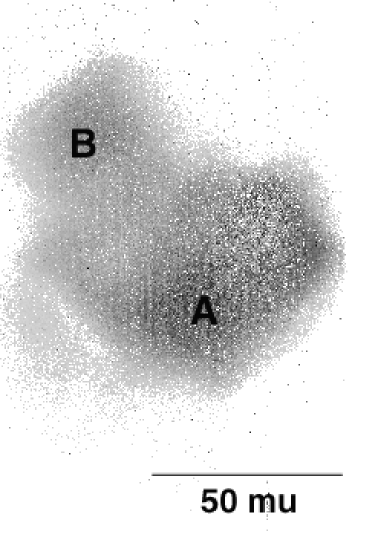
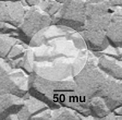
The same area of the diamond was scanned with a SEM and the SEM picture was correlated with the proton micro-beam measurement, as shown in fig. 13. Due to alignment and scaling uncertainties we estimate a matching resolution of .
Hot spots were found preferentially on cloven structures between grains. A remarkable large hot spot (see the arrow in fig. 13), which was stable under continuous irradiation, was located in the middle of the metallisation strip. The structure of this single hot spot is displayed in fig. 14 for different field strengths. The counting rate was reduced when the applied field was lowered and
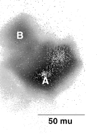
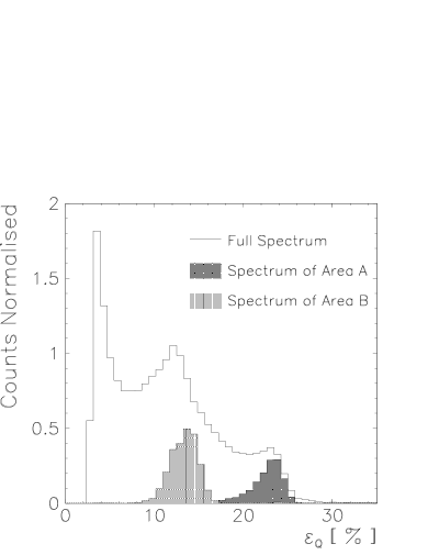
the corresponding spectra (fig. 15a) show a decrease in pulse height for lower fields. Two distinct peaks in the spectrum are observed, which are ascribed to two different areas in the hot spot. Fig. 15b shows the full spectrum of the hot spot and in shaded the spectra of area A and B at . Both spectra show clearly separated peaks. Area B is less efficient than area A. The peak position of A corresponds to a collection efficiency of about 25%.

Within the accuracy of the matching of the SEM-picture and the map we assigned the highlighted area shown in fig. 16 to this hot spot. The size of the highlighted area includes the estimated error on the matching. It shows that the hot spot sits most likely on the cloven structure as indicated in the picture.
We also scanned the substrate side of the diamond. The results of the substrate side gave a similar picture. Again the edges of the metallisation showed significant higher counting rates and hot spots appeared also on the substrate side. However, the population with hot spots was denser on the substrate side (spot density of about ) and they were smaller in dimension (typically to ) than on the growth side. This can be explained by the fact that the average grain size is smaller on the substrate side than on the growth side [13]. Furthermore, the existence of hot spots on the substrate side indicates that the surface roughness is not responsible for this phenomenon, since the substrate side was polished.
We tried to correlate maps of the growth side and the substrate side. If hot spots would appear at the same locations on the growth and on the substrate side it could indicate that continuous crystal columns of high collection efficiency are present at this locations. However, we could not observe a spatial correlation between the hot spot from the substrate and the growth side. This indicates that the lattice orientation or the crystal quality of the columnar structured crystallites are not a sufficient condition for a hot spot. The instability of some hot spots indicate a close link to polarisation phenomena as proposed by [24]. The result indicates that the crystallite orientation, quality and size are not sufficient conditions to produce a hot spot. The results favour the interpretation of a complex polarisation phenomenon at grain boundaries [24]. This view is supported by the spatially resolved measurement of with 10 keV photons, which ionise uniformly in the bulk and suppress polarisation. No enhancement of was seen with photons at the hot spot locations found with protons.
7 Summary and interpretation of the result
We have presented four experiments using different types of ionising radiation to investigate the charge collection properties of CVD diamond. In particular, we have used beta-particles of up to , a narrow beam of photons from a synchrotron source, alpha-particles and a proton micro-beam.
The samples show an increase of the charge collection efficiency, , when irradiated with beta-particles. The radiation dose needed to achieve saturation of this so called priming effect is different by a factor 15 between the two investigated samples. The relative improvements of ( for sample A and for sample B) are comparable.
To obtain information about the lateral distribution of , the signal spectrum recorded with beta particles was fitted with a smeared Vavilov-distribution which results in an intrinsic broadening of of for sample A (see section 3). This value is in good agreement with a direct measurement of the width and the spatial distribution of with a beam of photons, which measures for the same sample
In contrast, the response behaviour of the CVD diamond samples to mono-energetic alpha-particle and protons with stopping ranges of a few microns indicates a much higher value for . The particles produce a very broad pulse distribution with an exponential fall-off towards large pulse-heights. A strong polarisation build-up decreases the average value of and the counting rate during irradiation. This confirms observations reported in [12]. The spatially resolved measurement of with a proton micro-beam reveals single spots (hot spots) in the material with a high response embedded in passive areas, which is in agreement with observation made in [15, 24]. The shape of the hot spots and the correlation with SEM-pictures indicates that hot spots are bound to the crystallite structure. Since hot spots appear on the growth and on the polished substrate side we conclude that hot spots are neither caused by distinct surface topologies, nor require a certain crystallite size.
The most likely explanation seems to be that particular configurations of grain boundaries in the bulk, which are most likely to possess a high trap density [24], influence the polarisation field in the neighbourhood of single crystallites. The unstable behaviour of some hot spots and the good response on metallisation edges corroborates this assumption. As a result of this proposed complex and non-uniform polarisation, as seen by low energy particles is inhomogeneous. This is supported by the measurements with alpha-particles. The pulse distributions obtained with alpha-particles are compatible with the proton micro-beam measurements. Furthermore, the hot spots seen with the proton micro-beam do not show significantly higher values of compared to a photon beam. This suggests that the existence of hot spots is bound not only to a good crystal quality in this particular spot, but also to distinct features of the polarisation field in this area. The maps of obtained with a proton micro-beam are highly distorted by the local polarisation fields. Thus this method is not suitable to determine maps of for MIPs.
The observed increase of under irradiation with MIPs and the decrease of observed under irradiation with protons and alpha particles is not contradictory. In the former case traps are filled throughout the bulk thus increasing due to the decrease of active trap levels. However, because of the rather homogeneous distribution of the trapped charge no effective polarisation field is produced. In the latter case the majority of the charge is deposited in a shallow layer. In the electric field the charge carriers are separated and trapped and thus create a strong polarisation field. The polarisation is dominating over the increase of from trap passivation.
The applicability of CVD diamond as a particle detector depends on the radiation to be detected. For radiation which deposits charge inhomogeneously as in the case of alpha-particles, whose stopping range is much less than the film thickness, varies strongly and the stability is very poor. For homogeneous ionisation typically produced by MIPs or synchrotron-radiation at photon energies with , is stable if the detector is in its primed state, and a Gaussian-like distribution is observed. Thus, we conclude that CVD diamond has the potential of being used as a stable detector for homogeneous ionisation density distributions. However the relatively high value of might limit the achievable resolution of a position sensitive device.
References
- [1] L.S. Pan et al., J. Appl. Phys. 74 (1993) 1086.
- [2] F. Borchelt et al,NIM A354 (1995) 318.
- [3] T. Pochet et al., Conf. Proc. Vol. 52 “EURODIAMOND 96”, SIF, Bologna (1996).
- [4] G.J. Schouten, Distributor of Norton Diamond, Semi Dice, Wormeveer, Netherlands, private communication.
- [5] DeBeers Industrial Diamond Division (UK) ltd.
- [6] A. Bluhm, A. Oh, M. Paul, L. Schäfer, A. Wagner and W. Zeuner, contribution 15.099 to DIAMOND 97, Edingburgh (1997), to be published in Diamond and Related Materials.
- [7] J. Hassard and A. Howard, J. Phys. D - Appl. Phys. 28 (1995) 1279.
- [8] R. Hofstadter, Nucleonics (Apr.1949) 2.
- [9] S. Ramo, Proceedings of the I.R.E. (Sept.1939) 584.
- [10] K. Hecht, Z. Physik 77 (1932) 235.
- [11] R. J. Keddy, T. L. Nam and R. C. Burns, Phys. Med. Biol., Vol. 32, No 6 (1987) 751.
- [12] C. Manfredotti et al., NIM B93 (1994) 520.
- [13] W. A. Yarbrough and R. Messier, Science Vol. 247 (Feb.1990), 688.
- [14] S. Zhao, Ph.D. Thesis, Ohio State University (1994).
- [15] A. Oh, Diploma Thesis, University of Hamburg (1995), unpublished.
- [16] F.Foulon et al., IEEE Trans. Nucl. Sci. 41 (1994) 927.
- [17] St. Gobain Norton, Northboro, MA, USA.
- [18] Fraunhofer Institut für Schicht und Oberflächentechnik, Braunschweig, Germany.
- [19] Pole figure measurements have been carried out, Michael Zeitler, University of Augsburg.
- [20] Metallisations were carried out at [18].
- [21] S. M. Seltzer and M. J. Berger, Nuclear Science Series, Report No 39, (1964) 187.
- [22] B. Schorr, Computer Phys. Comm. 7 (1974) 215.
- [23] J.F.Ziegler, Hydrogen: Stopping Powers and Ranges in All Elemental Matter Vol. 3 (Pergamon Press, NY, 1977).
- [24] C. Manfredotti et al., Phys. Stat. Sol. (a) 154 (1996) 327.
- [25] The measurements with a proton micro-beam were carried out at the I. Institut für Experimentalphysik, University of Hamburg.