PERFORMANCE OF THE ATLAS-A SILICON DETECTOR WITH ANALOGUE READ OUT
Abstract
The performance of an ATLAS-A silicon micro-strip detector prototype with FELIX 128 analogue read out chip has been studied. The noise level and the signal to noise ratio have been measured as a function of both detector bias and temperature. No evidence of micro-discharge was observed for detector bias voltages up to 300 V.
UNIVERSITY OF LIVERPOOL
ATLAS
INDET–NO–xx
arch-ive/9606012
June 21, 1996
Physics Department, Oliver Lodge laboratory, University of Liverpool,
Oxford Street, Liverpool L69 3BX, U.K.
1 Introduction
The inner tracker of the ATLAS experiment at LHC will be built of silicon micro-strip detectors [atlas_tp]. These detectors have to operate in a high radiation level environment [rad_dose]. The effect of the radiation damage is basically an increase of the leakage current and a change in the effective bulk doping concentration. Therefore, a reduction of the signal to noise ratio and detector efficiency could be expected. In order to recover the expected performance after the detector has been irradiated, the simplest solution is to increase the bias voltage. However, some phenomena can limit the maximum value of the bias voltage applied on the detector [v_limit]. Then, the degraded performance of an irradiated detector could stand below the required minimum for a satisfactory operation of the ATLAS tracking system.
In the case of AC-coupled silicon detectors, micro-discharges [udq-japones] at the edges of the strips are one of the possible causes limiting the maximum value of the bias voltage applied on the detector. The micro-discharges are manifested as a steep increase in the noise level with an associated increase in the detector current.
The ATLAS-A detector design is based in -type strips on a -type bulk, because after radiation damage the lightly doped -type bulk inverts to a -type bulk with an effective doping that increases with dose. This leads to high values of the voltage needed to fully deplete the detector. This therefore could give a rise to micro-discharges.
In this note, the possibility of producing micro-discharges on an ATLAS-A silicon detector prototype has been tested. Therefore, the prototype performance has been studied at different biasing voltages (from 0 up to 300 V) and at two different temperatures (C).
The organization of this note is as follows: in section 2 the detector geometry and read out electronics are presented. Then the experimental set-up is described in section 3. In sections 4 and 5, the the experimental results in terms of the signal to noise ratio and the micro-discharge production are discussed. Finally, the conclusions are summarized in section 6.
2 Prototype and Read Out Chip electronics
The aim of this section is to describe the ATLAS-A silicon micro-strip detector, its technology and geometry, and the basic features of the FELIX 128 channel analogue read out chip.
-
1.
The detector used in our studies is a 6 cm 6 cm, with a 56.25 m diode pitch (with an isolation strip) and 112.5 m read out pitch (see figure 1). The strips are -type in a -type bulk, AC coupled. These strips are connected together to a bias ring through a polysilicon resistor (600 K). When biasing the detector the strips were directly grounded and the -type backplane was connected to a negative bias voltage. Both sides of the detector are surrounded by multiple guard rings. The guard rings are used to shield the sensitive part of the detectors and to provide a gradual drop of the edge potential, even after irradiation. Between the strips, a -stop isolation strip is used to avoid the short of the strips by accumulating positive charge in the SiO2 layer.
From the point of view of a possible production of micro-discharges, it is important to know the relative position of the implant and the metal contact [udq-japones]. In this case, the size of the metal contact is smaller by 2m (see figure 1).
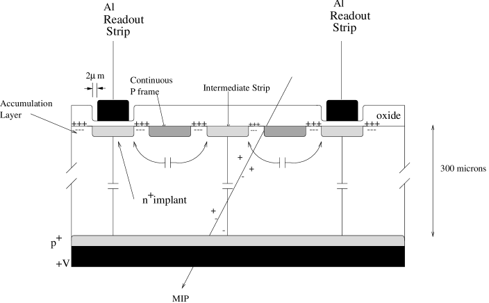
Figure 1: Cross section view of the ATLAS-A prototype. -
2.
The FELIX chip [felix] is a 128 channel integrated circuit designed to read out silicon strip detectors at the LHC. The architecture of the device can be broken down into 3 main blocks:
Front end pre-amplifier and shaper with a CR-RC characteristic of 75 ns peaking time.
An analogue pipeline, 1.6s deep (Analogue Delay Buffer).
An Analogue Pulse Signal Processor (APSP).
The chip has been designed to run in two modes:
Deconvolution: the charge collected is obtained from a suitable weight [deconv] of three 25 ns consecutive points measurements. It allows to extract the charge deposition in a single event, even in the case of pile-up of events. Therefore it can operate at high luminosity running at LHC.
Peak: The charge collected is obtained for each event from the measurement of the height of the signal pulse. It requires a minimum distance of 75 ns between two consecutive pulses, in order to avoid the pulse pile-up. Therefore this mode is inadequate for high luminosity running where the associated trigger rate is 25 ns.
3 Experimental Set-up
In this section the experimental set-up used for this study is described. It consists of the following three main parts:
-
–
Trigger system,
-
–
Data Acquisition System (DAS),
-
–
detector and FELIX biasing.
3.1 The Trigger System
The trigger system is based on the coincidences of two scintillators located above and below the silicon micro-strip detector (see figure 2). The coincidences can be triggered either by the MeV electrons of a radioactive source or by cosmic rays. In the second case a lead shield (used to stop the soft component of the cosmic rays [pdg]) replaces the radioactive source. Then, mostly single muons (minimum ionizing particles, m.i.p.) trigger the scintillators coincidence.

3.2 Data Acquisition System
The FELIX read out uses a VME Test System which is based around an MVME 167 Processor, with OS9 operating system. Within the VME crate there is a VME sequencer (SEQSI), a SIROCCO card with a flash ADC and a Random Trigger Card.
All clocks and control signals for the FELIX and the Analogue Multiplexor are generated by the sequencer. The Random Trigger Card is required to synchronise external triggers (e.g. the coincidence trigger from the scintillators) with the 40MHz BCO clock. Adjustment of the timing of this synchronised trigger relative to the data being collected is by means of a programmable delay unit. The data acquisition is by means of the VME SIROCCO where the analogue data is digitized and then written to disc.
3.3 Detector and FELIX Biasing
A Keithley 237 Source-Measure-Unit was used to supply a stable voltage for the detector biasing, and also allows the monitoring of the detector leakage current. Power supplies for the FELIX were provided by several low voltage bench power supplies, which also provided the biasing for the FELIX pre-amplifiers. It has been noticed that the performance of the FELIX 128 chip is strongly linked to variations on its bias power supplies. The main effects are: an increase in the noise level by a factor of , and/or a global shift of the pedestal values of all the channels.
4 Detector Performance
In this section the study of the detector performance is presented. Two types of particles were used to extract the signal to noise ratio. The first type is the muons from cosmic rays (considered as m.i.p). However the small trigger rate (hour) of these particles makes difficult to collect a large amount of events in order to perform precise measurements. Thus, a radioactive source emitting electrons of MeV was used instead.
A full range of bias voltages (from 30 V, just after depletion, up to 300 V) and two different temperatures (room C, and C) were used to determine the main factors affecting the resolution of a silicon micro-strip detector:
-
•
the noise level,
-
•
the signal to noise ratio,
-
•
the cluster size.
4.1 Noise Studies
4.1.1 Inter Strip Capacitance
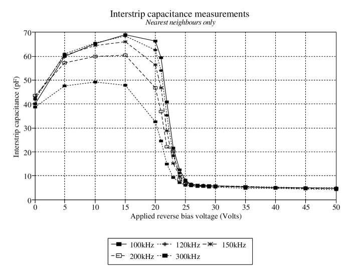
The inter strip capacitance is one of the most important parameters of the detector performance in terms of the noise level, and consequently in establishing the signal to noise ratio. In the cases of AC-coupled detectors, with integrated coupling capacitors, the measured capacitance is a convolution of both: the coupling capacitors and the direct capacitance between the implant layers.
The measured values for the inter strip capacitance of one strip to its two nearest neighbours, as a function of the bias voltage, are shown in figure 3. It is clearly seen how the inter strip capacitance is drastically reduced when the detector is fully depleted (25V). It falls to 5 pF, (equivalent to 0.85 pF/cm). Then, for higher bias voltages, it is almost flat, but the curves exhibit a small gradient when the voltage is increased.
According to this observation, the noise is expected to be reduced when increasing the bias voltage. Any deviation with respect to this behaviour could indicate new phenomena affecting the detector operation, like micro-discharges for instance, as they manifest them self as a sudden onset on the noise.
4.1.2 Effects of the Bias Voltage and Temperature on the Noise
The noise level in the detector has been studied as a function of the bias voltage and the temperature. The obtained values for both data sampling modes (peak and deconvolution) are shown in figure 4. One can appreciate as the noise is drastically reduced when the detector is fully depleted at V (in both data sampling modes). This behaviour is in perfect agreement with the observed one for the inter strip capacitance (read section 4.1.1). The achieved value for the noise is 15 mV in peak mode. The Equivalent Noise Charge was (ENC) was electrons.
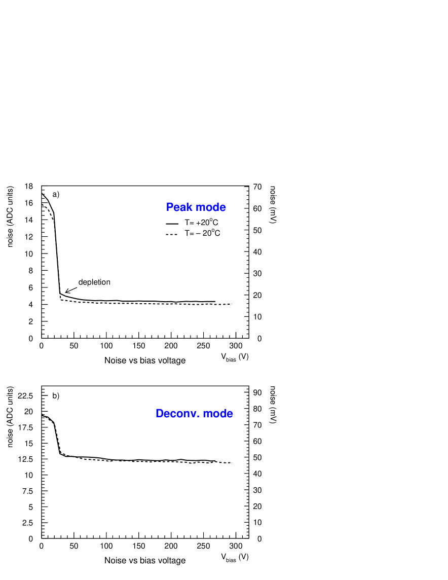
In figure 4 a slight decrease of the noise when increasing the bias voltage can be observed. The change is roughly a 10% in peak mode and a 12% in deconvolution mode. This can be understood as a consequence of the dependence shown by the inter strip capacitance on the detector bias voltage, and proves that our study is sensitive to small changes in the detector characteristics (section 4.1.1 and figure 3).
The noise of the detector exhibits a small dependence on the temperature. This effect can be observed in figure 4. As expected, the noise level is slightly reduced at lower temperatures. The reduction is a 7% for peak mode and a 4% for deconvolution mode. In the other hand, studies of the noise contribution from the read out electronics show that this is almost constant with the temperature. Consequently the noise reduction is due to the detector contribution, mainly due to a reduction of the leakage current (read section 5.1).
4.1.3 No Evidence of Micro-Discharges
From these results the production of micro-discharges in the ATLAS-A silicon detector prototype is discarded, as any onset on the noise in the detector have been observed, even at low temperatures where the effects are expected to be bigger if micro-discharges occur [udq-japones].
4.2 Hit and Cluster Search
In each event the impact point of the incident particles on the detector is obtained from a strip cluster search that proceeds as follows:
-
1.
the strip significance ( = charge collected in this event / noise) is computed for all the channels.
-
2.
Then, the primary strip is defined as the channel with the highest strip significance if .
-
3.
Those strips within an interval of strips around the primary strip with are included in the cluster.
-
4.
The hit significance is defined as the sum of the significance of all strips included in the cluster.
-
5.
The search for more clusters in the same event continues until no strips with remain.
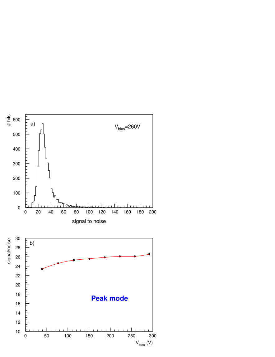
The signal to noise ratio is taken as the peak of the hit significance distribution, as it compares the charge collected in one strip with its noise and this is done for all the strips in a cluster.
The cluster size is just given by the number of strips in each cluster.
4.3 Signal to Noise Ratio
The values obtained in this analysis for the signal to noise ratio depend basically on the following factors:
-
•
data sampling (peak or deconvolution mode),
-
•
bias voltage,
Previous studies using the FELIX chip for analogue readout tests [chris_treshold] have shown that its performance in peak mode is better than using deconvolution mode (section 2). For this reason, only the results obtained in peak mode are presented in this section.
For a given bias voltage, temperature and read out scheme the only two magnitudes affecting the signal to noise ratio are: the collected charge (i.e. signal) and the noise level.
The collected charge depends on the incident particle type. In the case of muons (m.i.p.) the collected charge was equivalent to . In the second case, using the electrons from the radioactive source, the collected charge was slightly smaller, . The errors associated to both figures are mainly due to the calibration procedure. The ratio between muons and the MeV electrons of the radioactive source is: . In the ratio the systematic uncertainties due to the calibration are cancelled.
The collected charge has been seen not to depend on the bias voltage (once the detector has been fully depleted). This can be understood in terms of a constant efficiency for collection of the electron-hole pairs that have been created, once the detector has been fully depleted. This reflects that no extra charge is lost in the recombination processes inside the depleted zone, and this is not expected to be dependent on the bias voltage.
The noise level has been already studied in section 4.1, and as explained it is reduced when the bias voltage is increased.
The signal to noise ratio at 30 V reverse bias voltage and C was for muons and for electrons.
The amount of charge collected is the same for all bias voltage and the noise is lower for higher voltages, consequently the signal to noise ratio increases with the bias voltage (see figure 5.b). Using electrons as incident particles, the signal to noise ratio is .
4.4 The Cluster Size
In events with particles crossing the detector between two strips, only a fraction of the total produced charge is collected on each strip. Thus, the cluster size is in an important magnitude related with the spatial resolution of the detector. The worse resolution is obtained when all hits consist in a single strip cluster. Then the resolution is just given by: strip pitch/. For multi-strip clusters, it could be improved, if the impact point is just given by weighting the charge collected in each strip in a suitable way [a.peisert].
At different bias voltages, the electric field varies inside the detector. This electric field accelerates the charges towards the collector strips. So, for high values of the electric field, the expected behaviour is to collect a bigger fraction of the charge in a single strip. Then the spatial resolution is degraded.
The results obtained are presented in figure 6. The trend follows an increase of the fraction of clusters with a single strip when increasing the bias voltage. It varies from % of the events at low voltage, up to % at high biasing voltages. The absolute change is very small in a wide range of voltages. In consequence, the spatial resolution is not dramatically affected when using high bias voltage values. The fraction of clusters with at least two strips remains above the 80%.

The small dependence of the cluster size with the bias voltage is in part due to the charge sharing between the read out -strips propiciated by the intermediate strip.
5 Discussion
With the results presented in the previous section the micro-discharge production in the ATLAS-A prototype have been discarded. However, the leakage current on that device presents some peculiarities that need to be explained.
5.1 Leakage Current
The leakage current of the full detector has been studied in each step of the assembly process. The measured values of the leakage current are shown in the figure 7. In the case of the bare detector, two kinks can be appreciated in the I-V plot. These kinks are related with a change in the slope of the curve. These are reproducible phenomena, and the first kink (at V) matches quite well with the voltage for producing micro-discharges according to the reference [udq-japones]. However, there is no agreement in the absolute change of the current. Actually in reference [udq-japones], the micro-discharges originate a change bigger than two orders of magnitude.
Unfortunately, the wire-bonding process of the detector channels to the read out electronics had damaged the prototype due to the lack of a passivation layer. Therefore, after wire-bonding, the current is increased globally by a factor and the kink structure is lost.
In the other hand, the dependence of the leakage current on the temperature does not follow the expected one (approx a factor 1/2 each C) as shown in figure 7.a. As it is shown, the current is reduced just by a factor by changing the temperature by C. The temperature dependence of the leakage current for a fixed bias voltage is almost linear (see figure 7.b).

Neither breakdown nor punch-through in the leakage current is observed, and this is in agreement with a electric field being smaller than 30 V/m, which is supported by simulation studies using the semiconductor simulation package TOSCA [tosca].
It is believed that: the damage of the prototype when wire-bonding can not be responsible of a micro-discharge inhibition in the module.
6 Conclusions
The performance of an ATLAS-A silicon micro-strip has been studied using a FELIX chip with analogue read out. The signal to noise ratio (26:1) of the detector depends on the reverse bias voltage, as a consequence of the noise reduction. In the other hand, the cluster size shows that more than 80% of the cluster are multi-strip clusters. This two factors show that a good spatial resolution can be achieved with the ATLAS-A detector design.
No evidence of micro-discharges has been observed in this device, neither by burst on the leakage current, nor by a onset of the noise, even working at high bias voltages (up to 300 V), and low temperatures (C).