GLAS–PPE/95–06 R.L. Bates??) S. D’Auria??) S.J. Gowdy??) V. O’Shea??) C. Raine??) K.M. Smith??) A. Longoni??) G. Bertuccio??) G. De Geronimo??) 00footnotetext: Dept. of Physics & Astronomy, University of Glasgow, UK 00footnotetext: Department of Physics, Politecnico di Milano, Milano, Italy
On Behalf of the RD8 Collaboration
This paper presents current noise characterization of circular pad Schottky barrier diodes with guard rings. The diodes were fabricated from undopped semi-insulating GaAs, SIU-GaAs, at the University of Glasgow. Current noise spectra were obtained for the detectors for two pad sizes, with reverse bias applied. Three measurements were also made on one of the detectors under forward bias. The noise spectra show an excess noise component, with a low frequency corner at less than 1kHz, and a flat region at higher frequencies. The magnitude of the white noise is approximately half that expected from shot noise theory for the given leakage currents. A fall in the magnitude of the noise was observed at 20kHz which is attributed to the dielectric relaxation time of the material.
Presented by R.L. Bates at the workshop on GaAs detectors and related compounds
San Miniato (Italy) 19-21 March 1995
1 Noise theory
A detailed discussion of noise theory is given in references 1 and 2.
For any quantity X(t) that exhibits noise, the noise power within a unit bandwidth or power spectral density SX(f) is defined as
| (1) |
where X(f) is the Fourier transform of X(t), and is an ensemble average. In the simplest case where the transitions that cause the noise are described by equation (2), where is the lifetime of the fluctuation causing interaction, the spectral density is given by equation (3).
| (2) |
| (3) |
From simple statistical considerations () can usually be found, for example in the case of number fluctuations it is given by Poisson statistics.
This equation is very general with the condition imposed that the interactions of the electrons are independent. For small fluctuations this is indeed true and thus the Lorentzian spectrum (equation (3)) appears often. At low frequencies ( 1) the spectrum is white, that is independent of frequency, while at high frequencies ( 1) it varies as 1/, and its half power point is at f=1/(2).
1.1 Equivalent Noise Generators
In a two terminal network, noise in a frequency interval may be characterized using either an equivalent e.m.f. generator in series with the device or a current generator in parallel. An equivalent noise resistance, , and an equivalent noise current, , may be defined
| (4) |
where is the room temperature and is Boltzmann’s constant.

The equivalent circuit for a detector and amplifier system is shown in figure 1 and the noise components for an FET amplifier input stage are given below.
| (5) |
| (6) |
where is the transistor transconductance. The equivalent noise charge of a circuit with shaping time , is then
| (7) |
where and depend upon the type of shaping used. Thus an an optimum shaping time exists. If and are of similar magnitude and the leakage current term dominates, a short shaping time is required. The minimum obtainable equivalent noise charge may be limited by the 1/f noise if this term is large.
1.2 Types of noise sources
There are four noise source classifications in semiconductors: thermal, shot, generation-recombination, and modulation noise. The first three are well understood while the origin of the fourth with regard to semiconductors is less well so.
Thermal noise is a white noise source whose origin is based on fundamental thermodynamic physical laws. For a semiconductor of resistance R the spectral current and voltage noise densities are
| (8) |
Shot noise is due to the discreteness of the charge carriers and is related to the statistical nature of their injection into the semiconductor over a Schottky barrier. The origin of the spectral density may be found by considering Carson’s Theorem [1]. This states that for a diode with reverse current I which equals , where n is the spontaneously fluctuating number of electrons that cross the barrier per second, the spectral density is given by
| (9) |
It can be seen that the shot noise is linearly dependent on the frequency of the electrons crossing the barrier and quadratically dependent on the charge of the pulse that the electron creates in an external circuit. The spectrum is white because of the very short transit time of the carriers across the barrier, where the barrier includes the space charge region. For the barrier to show full shot noise at all frequencies two conditions must be met. The first is that when charge carriers are injected into the material, space-charge neutrality is re-established in a very short time, given by the material dielectric relaxation time [3], where is the resistivity of the material. For SIU-GaAs this is of the order of s. The second is that each current pulse should be able to displace a charge equivalent to that of one electron in the external circuit, that is to say a low trap density is required at the metal-semiconductor interface.
Generation-recombination noise can be understood by considering a semiconductor with a number of traps. The continuous trapping and de-trapping of the charge carriers causes a fluctuation in the number of carriers in the conduction and valence bands. The transitions are described by equation (2) and thus the noise spectral density is Lorentzian in nature, with a corner frequency given by , the lifetime of the electrons in the conduction band. The current noise density was calculated by van Vliet [4] to be
| (10) |
where . It should be noted that in observed spectra the corner frequency of this noise is dispersed, implying a wide distribution of lifetimes. If the current that flows through a device is due to generation then the expression for the noise present will be the generation-recombination one rather than the expression for the shot noise defined in equation (9). However in most Schottky junction devices the applied voltage will increase the injection rate and the noise will show a very close resemblance to shot noise.
At low frequencies an excess noise spectral density with a 1/f amplitude dependence is observed in semiconductors, which is known as modulation noise. As stated earlier the exact cause of this noise is still not understood.
2 The Diodes
The material used for the detectors was 200m thick semi-insulating GaAs. The detector fabrication was performed at the University of Glasgow. The detectors were designed with a circular pad contact and guard ring on top of the substrate. The bottom contact was a uniform contact that spread to the edge of the substrate. Two geometries were used, one with a pad diameter of 2mm the other of 3mm; the width of the guard was 200m and the pad guard separation was 10m for both diameters. The pad and guard metallization layers were identical and rectifying in nature. The reverse contact had a different recipe but was also rectifying, however its saturation current was larger than the pad’s due to its larger surface area. In the following, the direction of the detector bias is quoted with respect to that of the pad. Thus reverse bias means that the pad is at a negative potential with respect to the back contact.
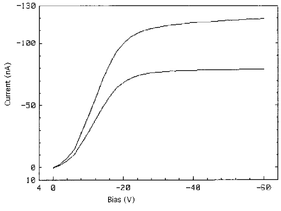
The I-V curves obtained for the diodes in reverse and forward bias are shown in figure 2.
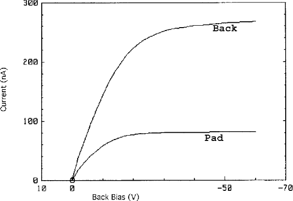
The purpose of the guard ring was to ensure that the current through the pad remained constant once in saturation. This was observed for all the samples, with the current that flowed through the pad, in the bias range 60 to 200 volts, increasing by only a few percent. For a given bias the current densities of both pads were the same and equalled 25nA/mm2. The results showed that the saturation current density that flowed through the pad under forward bias was the same as that obtained in reverse bias.
3 Measurement Procedure
To measure the current noise of the diodes under an applied bias an amplifier designed by the Politecnico di Milano was used [5]. This had a large bandwidth (), high gain (), low noise () and an adjustable input bias offset. The amplifier had a large input impedance (1G) and a low output impedance (). This amplifier was used as an operational amplifier with a feedback resistor and a feedback capacitance . The output of the amplifier was passed through the high impedance input of an AC coupled oscilloscope and out through the ’scope’s output. The ’scope thus acted as a low noise voltage amplifier. The output of the ’scope was sent to a HP signal analyser with input impedance. The feedback resistor was chosen to maximize the gain of the amplifier (large ), minimize the background noise due to the thermal noise of the feedback resistor (large , see equation (8)) and to make sure that the amplifier did not saturate (limits ).
Before the current noise density spectra of the diodes were measured the transfer function and the background noise of the amplifier were determined. The transfer function was required so that the measured voltage noise could be referred back to the input as a current noise. Background noise measurements were made to show that the noise contribution from the ’scope was negligible and that the overall background noise present in normal operation was close to the thermal noise of the feedback resistor.
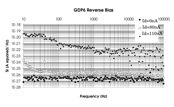
Noise spectra were obtained for both diodes, at zero bias, under reverse bias, at the same leakage current for both diodes and under forward bias for the small diode at three leakage currents equivalent to those used for the reverse bias case.
4 Results
In this section the current noise spectral densities of the diodes are shown and some tentative interpretations of the results are proposed.
At zero bias the measured noise is the thermal noise of both the feedback resistor and the diode. From equation (4) the equivalent noise resistances of the diodes were found which with the use of the diode dimensions enabled resistivities for the material of 12.4Mcm and 18.3Mcm to be obtained. Both values are of the correct order of magnitude.
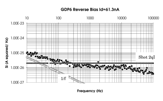
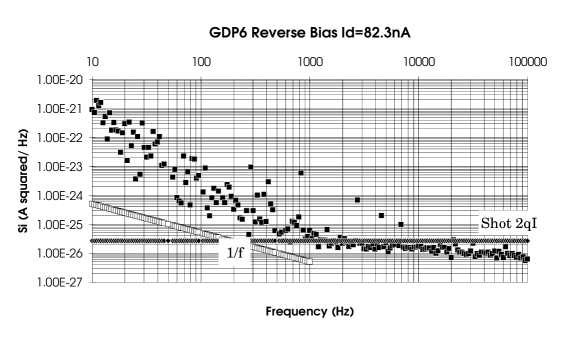
Figure 4 shows a typical noise spectrum. All the spectra are white at frequencies above the corner frequency of the excess noise. The value of the current noise density is less that that expected from equation (9). At a frequency of 10kHz the noise over the measured leakage current range is between 1.7 and 2.3 times less than the simple shot noise theory. At frequencies between 20kHz and 30kHz there is a corner in the white noise.
If the leakage current is due to the thermionic emission of carriers over the Schottky barrier then the noise should be shot noise. A simple model can be devised to explain the shot noise spectra obtained, with reference to equation (9) and figure 3. One can say that if an electron is trapped and at a later instant released then this electron will produce two pulses of charge whose sum is equal to e. If the electron is captured after producing a charge pulse equal to in the external circuit and then released, on average the frequency of charge pulses produced by the emitted electrons is doubled while the charge is halved. The shot noise spectral density is thus reduced by a factor of two. Shot noise should be white due to the fast transit time of the electrons across the high field region behind the reversed biased Schottky junction, however, this is not observed. The corner frequency at 30kHz can be explained with reference to the condition imposed that charge neutrality is obtained in a time given by the dielectric relaxation time. Assuming that the noise source is Lorentzian, the corner frequency corresponds to the reciprocal of this time constant. Thus a lifetime of the order of 10-5s is required, which is equivalent to the dielectric relaxation time in SIU-GaAs.

If the major contribution to the reverse bias leakage current is the generation current, rather than the injection of carriers over the Schottky barrier then the noise is due to generation-recombination noise from the bulk and not thermionic emission at the barrier. The noise due to generation has a characteristic time constant, the lifetime of the generated electron in the conduction band, which is inversely proportional to the corner frequency of the spectrum. If the transport mechanism is said to be by relaxation processes then the lifetime, in equation (10), is the dielectric relaxation time. Although, in principle, the dependence of the measured spectral density on the leakage current should help separate the two causes of the white noise, no clear dependence was observed.
The final part of the diode noise spectrum is the low frequency excess noise. This is seen for measurements made on the small diode for currents up to 70nA (75V bias) as approximately 1/f noise which meets the white noise at a frequency of 500Hz. At 10Hz the excess noise is an order of magnitude greater than the white noise component of the spectrum. This is also observed in the large diode for currents up to 170nA (50V bias).
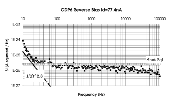
At larger currents (above 71nA for the small diode) a second low frequency noise component appears which has a much steeper frequency dependence, where is close to 3. At 10Hz the excess noise is now almost two orders of magnitude larger than the white noise. (figure 5).
The magnitude of the excess noise is seen to increase with bias towards the ‘breakdown’ of the diode. Here the corner frequency of the excess noise extends to much higher frequencies; 1kHz @ 230V, and 100kHz @ 240V for the small diode. The magnitude of the noise increases dramatically, to reach 310-21 A2/Hz at 10Hz at 230V for the small diode (see figures 6 and 7). At a bias of 200V the electric field extends across the sample to the forward biased contact which causes charge injection and thus the dramatic increase in the measured noise which occurred between 230V and 240V.
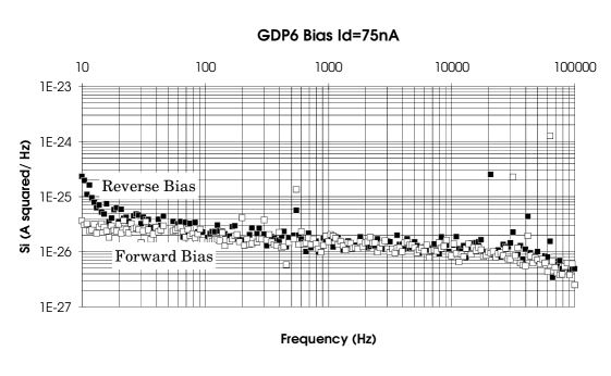
Noise spectra for the forward biased diode are similar to those obtained in reverse bias as shown in figure 8. The white noise component is approximately the same, the high frequency corner is present, but no low frequency excess noise is present in the forward biased case. The reason why no excess noise is seen for the forward biased diode is not clear.
5 Conclusions and Future Work
The noise measurements show three distinct regions in the spectra, the first being the low frequency, , excess noise which has a corner frequency of 500Hz for bias voltages below 75V. Above this the excess noise has a second component which is steeper, being almost in nature, and has a corner frequency of 50Hz which increase with bias. As the diode approaches breakdown the corner frequency and the magnitude of the excess noise increases dramatically due to injection at the forward biased contact. The second feature of the spectra is the lower than expected value of the shot noise, being about half that of simple theory. This is due to trapping of the charge carriers in the bulk which reduces the amplitude of the individual pulses that the carriers produce while increasing their frequency. The third region is the corner frequency of the white noise between 20-30kHz. This is noted to be close to the reciprocal of the dielectric relaxation time for SIU-GaAs.
Further noise measurements need to be made on more samples using different types of contacts to see if there is any correlation between the noise of the sample and the properties of the material and fabrication. Diodes that have been irradiated also need to be tested to improve the present understanding of the effects of irradiation. The technique can also be extended to examine strip detectors made from GaAs. The biasing structure used at present utilizes a punch-through mechanism via a MSM diode. There is a possibility that this may introduce more noise and it is important to understand if this is true.
6 Acknowledgements
The authors wish to express their appreciation to A. Meikle, F. Doherty and F. McDevitt of the University of Glasgow for their fabrication skills.
References
-
[1]
Van der Ziel: Fluctuation phenomena in
semiconductors
Butterworths Scientific Pub., London, (1959). -
[2]
M.J. Buckingham: Noise in electronic devices and
systems
John Wiley and Sons, London, (1983) -
[3]
S. M. Sze: Physics of semiconductor devices
J. Wiley, New York, (1991). -
[4]
K. W. Boer: Survey of Semiconductor Physics
Van Nostrand Reinhold, New York, (1990). -
[5]
A. Longoni et al.: To be published.
Department of Physics, Politecnico di Milano, Milano, Italy.