GLAS–PPE/95–05
In this paper we present a method for simulating the response of microstrip detectors to minimum ionizing particles, making use of a program for field calculation, a program for carrier drift and SPICE for circuit response. A knowledge of the electric field is essential for any further improvement of the program. A simple model involving EL2 levels in the metastable state is proposed to explain some measurements of electric field.
Presented by S. D’Auria at the workshop on GaAs detectors and related compounds
San Miniato (Italy) 19-21 March 1995
1 Introduction
Microstrip detectors made of GaAs will be used in a part of the forward tracker detector in ATLAS at the LHC because of their larger radiation hardness when compared to silicon devices. Test beam results are reported elsewere in these proceedings. In order to optimise the parameters of the devices, such as total thickness, strip pitch and aspect ratio for a required spatial resolution, we are developing a program which is able to calculate the current signal from the various geometrical configurations and crystal properties. A more detailed study will be published later; in the following we describe the method and stress the importance of a detailed knowledge of the electric field inside the detector.
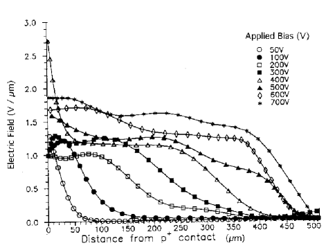
The second part of this paper deals with a model for the electric field. Semi-Insulating-Undoped (SIU) GaAs has a resistivity of the order of which is achieved through a compensation by deep levels. These levels are mainly of the intrinsic type called EL2, which is due to the non perfect stoichiometric ratio between Ga and As. In detectors made of this material the region which is active for detection has a thickness which increases with bias. At a bias of 200 V about 180 are active [1, 2, 3]. Various models [4, 5, 6] have been proposed to calculate the electric field, and two measurements have been made [7],[8]. The measurements show that the electric field is approximately uniform at high voltages, which means that the sensitive region has a very low fixed charge density. This observation is very difficult to explain in homogeneous materials, where the fixed charge density is constant over the depth. A possible explanation of such a field shape is that some of the EL2 defects, under the influence of a strong electric field, make a transition to a normally metastable state featuring no energy levels in the forbidden gap. The existence of such a level has been reported [9], but neither evidence nor exclusion of a voltage-induced transformation has yet been reported.
2 Microstrip detector simulation
SIU GaAs is characterized by an imperfect drift of charge carriers, due probably to trapping [10] and to the peculiar shape of the electric field. Double-sided microstrip detectors show a marked asymmetry in charge response from the two sides [11]. Therefore a full 2-dimensional simulation of the charge drift in the device is needed in order to calculate the signal induced on the strips.

The chain of programs used is shown schematically in fig. 1. The three main parts are: a program to calculate the electric fields, one to simulate the drift of electrons and holes, and finally a SPICE calculation of the response of the front-end network. Each of these parts will be considered separately.
2.1 Field calculation
In simulating a device two or more electric fields have to be considered [12]. They are the physical field which is driving the motion of charges and the so called weighting field which has dimensions and is a purely geometrical function of space position. It is a measure of the coupling between the moving charge and the electrode considered. For instance, in the simple case of parallel-plate diode electrodes separated by a distance the weighting field is a vector of length perpendicular to the surface. In the case of devices with more electrodes, as in microstrip detectors, the weighting field for the jth electrode is calculated by holding it at +1 V and mantaining all the other electrodes at ground. All the fixed charge has to be neglected.
In the first stage of work reported here we have used the code GARFIELD [13] to calculate the electric fields. This program was written to simulate gas operated multiwire drift chambers. A part of it performs a 2-dimensional calculation of electric field in a configuration where electrodes have a wire shape or are infinite planes.
Each microstrip was simulated as an array of neighbouring wires with a distance between centres 1% larger than their diameter. We then checked that the resulting field was independent of the wire diameter and we chose a diameter of as a good compromise. A clear limitation of this method is the lack of simulation of surface effects with dielectric materials such as silicon nitride and air. Also, we expect that results are reliable only on a scale larger than a few times the wire diameter. This is acceptable if signals from minimum ionising particles (m.i.p.s) have to be simulated, but a more accurate calculation of the field is needed if details have to be looked at or if signals from alpha particles are to be simulated.

A plot of the modulus of the weighting field for one strip is shown in fig. 2. The major contribution to the signal for that particular strip is due to holes or electrons moving in proximity of it. Due to the geometry, however most of the signal is due to holes.
The drift field was calculated by GARFIELD and then multiplied by the following function:
| (1) |
where x is the distance from the strip plane, is the thickness of the active region, is the thickness of the transition region. A low overall constant field of 100 V/cm was then added. The result is an approximation to the field measured in ref. [7], (fig. 3). It was assumed that with , as reported in [2].
As an example, a zone of 550 in width for a 200 thick detector was simulated. The strip pitch was 50 and the metal width was 40 . Only the part comprising 5 central strips was used for further analysis corresponding to a grid of points. Interpolation of the electric field was used between points.
2.2 Drift of charge carriers
The initial distribution of charge is assumed to be uniform along the linear track of a minimum ionizing particle. Genaration of delta rays and charge spreading has not yet been implemented, but is assumed to be not essential at the present stage. A constant number of electron-hole pairs is generated for each track. A time-slice approach is used in simulation, as a current signal is required. Each individual carrier is followed during its drift. Trapping probabilities are calculated from the trap concentrations , , cross sections and drift velocity . A flag associated with each carrier indicates its status, which can be: free, trapped, reached the electrode. The probability of being trapped by the kth type of trap is given by:
| (2) |
where is the time step.

Detrapping is also taken into account as a possible process. We assume that there is a mean trapped time and that both and are independent of electric field.
The carrier drift velocity is calculated from the electric field using parametrizations of the experimental data [14][15], as shown in fig. 4. We note that provided the field is high enough, the details of its shape have a negligible influence on carrier velocity for the larger part of the device, as saturation is reached. If drift in a magnetic field and diffusion have to be considered, however, an exact knowledge of the electric field is essential.
The current signal on the jth electrode is calculated from the Ramo-Shockley theorem:
| (3) |
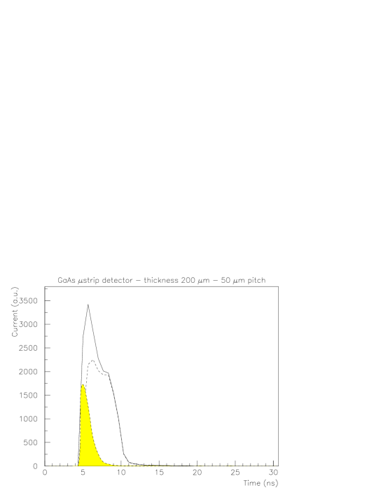
where is twice the number of electron-hole pairs generated, is the weighting field and the charge of the carrier. The charge signal is obtained by integration of and gives the charge collection efficiency. An example of a current signal is shown in fig. 5 and is used as input for SPICE.
2.3 SPICE calculation
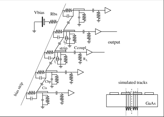
In order to calculate the signal reaching each preamplifier the front-end and bias coupling network was simulated using SPICE. The parameters depend mainly on the detector geometry. The main parameters are the inter-strip capacitance, depending on pitch, aspect ratio and strip length, the strip to back contact capacitance and the decoupling capacitance. The biasing structure, based on punch-through was also included as a 10 G resistor with a 20 fF capacitance in parallel. A schematic is shown in fig. 6. Resistors had to be used to ensure a DC path to nodes.
The signals from two neighbouring strips were included as two independent piece-wise linear current generators. The current values were calculated with the drift code described previously, simulating tracks impinging perpendicularly on the strips; the hit position was varied from the centre of the central strip to the centre of the neighbouring one on the right. It was assumed that all strips were read-out. In simulating the signal a symmetry relation was assumed, i.e. where is the pitch, and is the distance of the track from the centre of the strip.

The current signal at the preamplifier input was calculated and then integrated to give the total charge detected by each channel. An function [16], related directly to spatial resolution could be calculated for the given configuration. An example is shown in fig. 7.
3 A model for the electric field
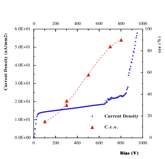
The present simulation chain can be a starting kernel for further improvements. However, a more detailed simulation, including effects of magnetic field and diffusion, is possible if a definite shape of electric field is generally accepted. Measurements made at UMIST [7] indicate that the field is uniform in the vicinity of the reverse biased contact, as shown in fig 3. This a clear experimental result. Most calculations [4] [5] result instead in a linearly decreasing electric field. This arises naturally if a uniform doping concentration is assumed. Although some of the defects are not ionized due to quasi-Fermi-level shifting by the reverse bias current, the main trend is a field decreasing monotonically to the back contact. A constant electric field is quite difficult to explain. A correlation between reverse current and charge collection efficiency for alphas has been reported as evidence supporting the calculations. This correlation has not been found by us for m.i.p.s, as we have several examples of detectors with a low reverse current density (20 nA/mm2) and high charge collection efficiency (90 %) over a large thickness (500 ) (fig. 8).
Another model [6] proposes a neutralization of deep levels by field-enhanced trapping of the electrons of the reverse current. In this model, too, a high current is required to obtain a high charge collection efficiency.
The nature of the reverse current is not yet clear. Thermionic emission would require a really low barrier height, while if a generation mechanism is assumed, saturation could normally be explained only if most of the current is generated in the first few micrometers below the reverse-biased contact. Otherwise the current density is expected to increase with the volume in which the electric field is high.
Commercial SIU-GaAs usually contains a concentration of about cm-3 of EL2 defects. This defect is believed to be due to an As substitutional () plus an As interstitial () as second nearest neighbour [17]. The material is naturally compensated and shows a resistivity of cm which is ideal in a substrate for electronic and optical circuits.
The EL2 defect has been reported [9] to have a metastable state EL2∗ which has very little or no electrical and optical activity. It is therefore believed that the corresponding energy level is split and shifted into the conduction and valence bands. One proposed microscopic structure of EL2∗ is similar to EL2, but with the atom as nearest neighbour. the transition is:
| (4) |
The EL2∗ can be generated via optical absorption, involving different charge states [18]. The decay rate to the stable state has an activation energy of 0.3 eV so that at room temperature the metastable state has a lifetime of about . It is generally observed at fairly low temperatures, (about ) and in the presence of a low electric field.
If the transition could happen at room temperature, under the effect of a high electric field, for example, the measurements of electric field shape in [7] could be qualitatively explained in the following way: as reverse bias is applied, deep donors start to become ionized; some are neutralized by trapping electrons from the leakage current, as in [6]; this lowers their effective concentration, in such a way that the electric field can extend for several micrometres. This process continues until the field at the contact reaches a critical field, , of about 10 kV/cm, at a bias voltage between 20 and 50 V. At this point the transition EL2 EL2∗ starts to take place, so that the field remains roughly constant, as deep levels are no loger active. We should assume that the transition is not complete, leaving some compensating EL2+. The region where the field drops is shifted rigidly towards the back contact as bias is increased. In this transition region the electric field is non-zero and most of the EL2 defects are active. Thus the reverse current can be efficiently generated there and is constant to the extent that the transition region has a constant thickness while moving across. This is to be expected in a homogeneous material. A sketch of the proposed model is shown in fig. 9.
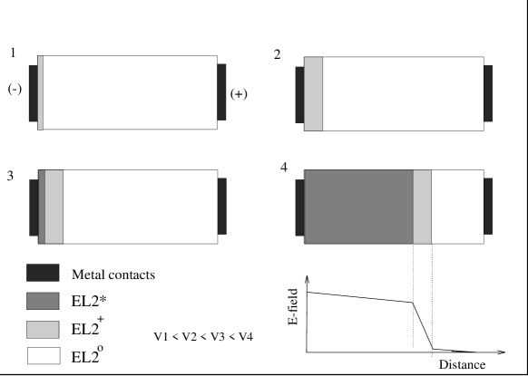
From the point of view of charge transport, three regions of electric field can therefore be distinguished: one constant, one linearly decreasing and one with an extremely low residual electric field. This is quite similar to that shown in fig. 3. In the third region transport is mainly due to charge relaxation, with a typical time of , giving a slow signal component. In the transition region the field is decreasing. Thus the electron velocity initially increases then decreases and trapping can be enhanced. The charge collection efficiency and the medium-slow components of the signal depend on the shape of the field. In the region where a constant field is present the charge transport is good, as the concentration of active traps is lower. Little contribution to trapping is expected from this zone.
The shape of electric field used in the simulation now has also a theoretical (although qualitative) explanation and is not based only on empirical data. While the validity of this model is not proved, it enables to explain consistently many features of SIU-GaAs detectors. C-V characteristics would not characterise this model, as the transition region where charge can move has the same features as in normal semiconductors. The saturation of reverse current can be explained in this model, assuming that the current is generated mainly in the transition region where the electric field is non negligible and the concentration of active levels is high.
A possible way to test the model is with OBIC measurements [2] using a focused light beam at a wavelength which is unable to separate directly an electron-hole pair. In this way only deep levels will be probed and the photocurrent at a distance from the front contact will be proportional to the number of active levels at that point and to the electric field. A region of constant width where the photocurrent is higher is expected to move across the detector as the reverse bias is increased. If the model is incorrect the region with high photoresponse will simply increase in width. We propose to carry out this measurement in the near future.
4 Conclusions
A code has been set up to simulate the response of GaAs microstrip detectors to m.i.p.s. From preliminary results it is evident that charge sharing is possible in principle also in SIU-GaAs detectors where the charge transport is not perfect, provided that the strip parameters and noise performances are optimized. More extensive results on various geometry and parameters will be presented soon. Limitations of the present code are in the calculation of details of the electric field near the strip and at the interface with passivating layers. This will be improved using a more suitable package for the field calculation. Further developments will also aim at including the possibility of drift in a magnetic field and the effects of diffusion. Because of the peculiar band structure of GaAs these processes are strongly dependent on the local intensity of the electric field even when the drift velocity is saturated. A detailed knowledge of the electric field is needed to improve the simulation.
A possible explanation of the measured electric field profile has been proposed, based on a transition of the EL2 defects which makes them electrically and optically inactive. This model can explain consistently a variety of features of SIU-GaAs, like the slow transients and a saturation in generation current.
Acknowledgements
We wish to thank PPARC and the EC (via an H.C.M. contract) for support and our host for organizing this workshop.
References
-
[1]
S.B. Beaumont, R. Bertin et al.:
Gallium Arsenide detectors for minimum ionizing particles
Nucl. Phys. B (Proc. Suppl.) Vol 32 (1993) 296-299. -
[2]
A. Cavallini et al.:
An optical-beam-induced-current study of active region and charge collection efficiency of GaAs particle detectors
Nucl. Instr. and Methods in Physics Research A 355 (1995) 420-424. -
[3]
F. Nava, C. Canali, A. Cavallini et al.:
Influence of electron traps on charge-collection efficiency in GaAs radiation detectors Nucl. Instr. and Methods in Physics Research A 349 (1994) 156-159. -
[4]
T. Kubicki, K. Lubelsmeyer, M. Toporowski et al.:
calculation of the electric field in GaAs particle detectors Nucl. Instr. and Methods in Physics Research A345 (1994) p. 468. -
[5]
J. W Chen, T. Froemmichen et al.:
Evaluation of active layer properties and charge collection efficiency of GaAs particle detectors
Submitted to Nucl. Instr. and Methods A -
[6]
D. S. McGregor, R. A. Rojeski, et al.:
Present status of undoped semi-insulating LEC bulk GaAs as a radiation spectrometer
Nucl. Instr. and Methods A343 (1994) 527-538 -
[7]
K.Berwick, M.R.Brozel, C.M.Buttar, M.Cowperthwaite and Y. Hou:
Studies of charge collection in GaAs radiation detectors
Mat. Res. Soc. Symp. Vol 302 (1993) 363-368. - [8] J.J. Mares et al. to be published
-
[9]
C. Delerue, M. Lannoo, D. Stievenard et al.:
Metastable state of EL2 in GaAs
Phys. Rev. Letters 59 (1987) 2875-2878. -
[10]
S. P. Beaumont, R. Bertin et al.:
Gallium Arsenide charged particle detectors: trapping effects
Nucl. Instr. and Methods in Phys. Research A 342 (1994) 83-89. -
[11]
S. P. Beaumont, R. Bertin et al.:
First results from GaAs double sided detectors
Nucl. Instr. and Methods in Phys. Research A348 (1994) 514-517. -
[12]
E. Gatti, P. F. Manfredi:
Processing the signals from solid-state detectors in elementary-particle Physics
Rivista del Nuovo Cimento 9 n. 1 (1986) 1-147. -
[13]
R. Veenhof:
Garfield, a drift-chamber simulation program - User’s guide CERN (1994). -
[14]
J. C. Ruch and G. S. Kino:
Transport properties of GaAs
Phys. Rev. 174 (1968) 921. -
[15]
V. L. Dalal, A. B. Dreeben, A. Triano:
Journal of Appl. Physics, 42 (1971) 2864. -
[16]
R. Turchetta:
Spatial resolution of Silicon microstrip detectors
Nucl. Instr. and Methods in Phys. Research A335 (1993) 44-58 -
[17]
J. C. Bourgoin, M. Lannoo:
A critical look at EL2 models
Revue Phys. Appl. 23 (1988) 863-869 -
[18]
R. Kiliulis, V. Kazukauskas:
Model of charge transfer induced by EL2 EL2∗ transformation in Semi-Insulating GaAs
Phys. Stat. Sol. (b) 180 (1993) 155-162.