A First Mass Production of Gas Electron Multipliers
Abstract
We report on the manufacture of a first batch of approximately 2,000 Gas Electron Multipliers (GEMs) using 3M’s fully automated roll to roll flexible circuit production line. This process allows low-cost, reproducible fabrication of a high volume of GEMs of dimensions up to 3030 cm2. First tests indicate that the resulting GEMs have optimal properties as radiation detectors. Production techniques and preliminary measurements of GEM performance are described. This now demonstrated industrial capability should help further establish the prominence of micropattern gas detectors in accelerator based and non-accelerator particle physics, imaging and photodetection.
keywords:
GEM , Radiation detectors , Gas filled detectorsPACS:
29.40.-n , 29.40.Cs , 29.40.Gx , 95.55.Vj , 85.60.HaA number of new radiation detector designs, collectively referred to as Micropattern Gas Detectors (MPGDs) [1, 2] have recently emerged in response to the extraordinary demands of next-generation High Energy Physics (HEP) experiments, namely the ability to respond to a high counting rate and integrated particle flux, superior radiation resistance and fine spatial resolution. Common to these designs is the presence of a large voltage drop (several hundred volts) across microstructures immersed in a suitable gas mixture. Electrons originating from ionization of the gas in a conversion volume drift to the region of the microstructures where the intense electric field allows gas amplification to occur. Due to the confined amplification regions, slow positive ions are removed immediately from the amplification volume, increasing rate capability by several orders of magnitude compared to wire based gas detectors.
The attractive features of these detectors have lead to a growing number of applications in many fields. For instance, MICROMEGAS chambers [3] can be found nowadays in medical digital X-ray imaging equipment [4], where a high sensitivity in low intensity radiation fields results in a diminished dose to the patient, while profiting from an enhanced image contrast. Similarly, photocathode-coated MPGDs promise to surpass photomultiplier tubes in light detection efficiency, reduced cost and speed [5, 6]. Other emerging applications are industrial imaging [7] and X-ray astronomy [8]. Reviews of these can be found in [1, 9].
Recently it has been proposed to extend MPGD use to the field of non-accelerator particle physics [10, 11], where uses would be numerous in view of their simplicity, the possibility to easily construct MPGDs out of radioclean materials and their very low energy threshold. It is in the context of the development of a new type of neutrino detector [11] that we attempted to manufacture MPGDs in large numbers and with near-perfect reproducibility, using an industrial approach. This effort may nevertheless have repercussions in satisfying the large demand for MPGDs in accelerator based physics. For this first attempt we chose a popular design, the Gas Electron Multiplier (GEM) [12] given its particular simplicity of design. A GEM consists of a -thick polyimide (KAPTON) film copper clad on both sides, perforated with a regular matrix of small holes (diameter few tens of m) produced by photolithography. When a voltage difference is applied between the two sides of the GEM, a large electric field is produced in the holes. Electrons that enter the holes undergo gas amplification. A remarkable advantage of GEMs is the possibility of building multi-stage amplification layers [13], where electrons are transferred from one GEM to the next, undergoing successive avalanches and yielding very large charge gains. The resulting high-efficiency for single electron detection looks particularly attractive to us, when considering the small energy depositions expected from low-energy neutrino recoils [11].
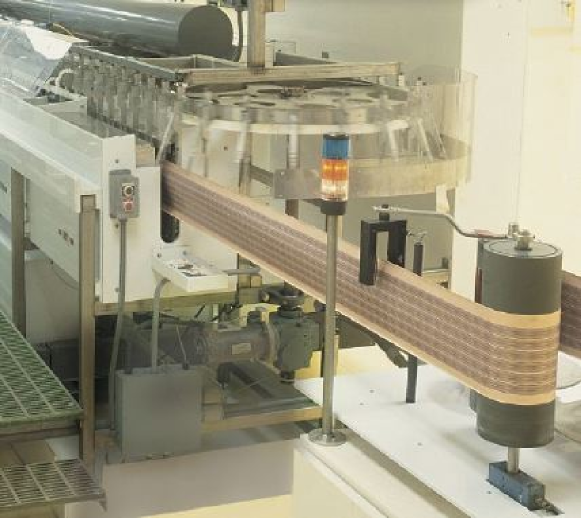
We report here on preliminary tests and observations made on a first batch of GEMS (Fig. 1) produced using 3M’s high volume, wide web, roll to roll, adhesiveless flexible circuit (FLEX) circuit making process (Fig. 2). At the time of this writing every indication points at their having a satisfactory performance as radiation detectors. Our preliminary results are encouraging but testing is in an early stage. For example we have not yet studied the resistance to radiation (ageing) of the GEM. We however feel that the widespread demand for GEMs by numerous research groups justifies the early release of our findings.
Flexible circuits are utilized in a variety of applications such as inkjet printer cartridges, hard disk drives, liquid crystal display modules, and IC packages among others [14]. These applications have a variety of needs that are met with various FLEX circuit constructions. These can be grouped into two categories: 3-layer and adhesiveless FLEX circuits [15]. A 3-layer FLEX is appropriately named since it is constructed from a copper foil, a polymeric film, and an adhesive to bond foil to film. In many applications such as Hard Disk Drives and GEMs, the presence of the adhesive would create outgassing and ionic problems. An adhesiveless FLEX circuit (also referred to as a 2-layer FLEX) requires alternative means for securely bonding the copper to the polymer. The two primary methods for fabricating an adhesiveless FLEX circuit are a) direct metallization of the polymeric film and b) casting of liquid polyimide onto the Cu foil. After the substrate has been created, the copper and polyimide materials must be patterned to form the desired geometry for the application. The copper pattern can be formed by using either an additive or subtractive circuitization process. The process flows for each are illustrated in Fig. 3.
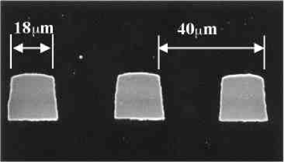
The additive process consists of applying a photo resist imaged with the desired copper pattern to a -thick polyimide film, directly metallized on both sides. The copper is then electroplated to the appropriate thickness onto the exposed flash layer. This plating technique can allow for a wide range of copper thicknesses ranging from 4 to 36 m. As shown in Fig. 4, this additive circuitization process can achieve very fine copper features [16], down to trace and space on 1-metal layer FLEX circuits ( traces and spaces on 2-metal layer FLEX circuits). As can be seen in the trace cross section in the figure, the sidewalls on the additive copper are nearly vertical.
GEM foils were also manufactured using the subtractive process flow outlined in Fig. 3. The subtractive structure is believed to be similar to the construction described by Bouclier et al. [17]. The side walls of the copper openings have a somewhat shallower slope than in the additive process. GEMs produced with these two different circuitization processes showed some performance differences described below.
One lot from each fabrication method has been produced so far, each containing 30 identical panels of 33 GEM elements (Fig. 1). Production of a much larger number of panels per lot, up to a few hundred, is possible. In both cases the chosen design was the so-called “standard GEM” [18], i.e., m holes in an hexagonal pattern with m pitch and a biconical transversal hole cross section. In other words, the innermost part of the holes exhibits a reduced opening of m, a characteristic also found in most GEMs built elsewhere. The use of Dupont E-film KAPTON as the substrate does not allow to reduce this opening any further. In present lots the copper thickness was fixed at m to insure the success of these first trials. In successive attempts this will be further reduced, a feature of interest for tracking devices where multiple scattering in the detector must be minimized.
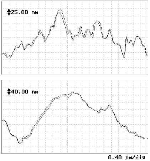
The surface quality of both lots has been studied via SEM (Fig. 5) and AFM (Fig. 6). Slight copper opening irregularities are observable mostly on one side of these first additive GEMs. This may lead to gain inhomogeneities across the GEM surface: therefore we have concentrated at first on the characterization of the subtractive lot. The additive fabrication process has proven to be challenging: small polyimide ribs stemming from the interior of the holes were initially observed to envelope the edges of copper openings. Additional treatment of the lot removed these but resulted in a slightly diminished copper to polyimide attachment111It must be noted that the method used to test copper to polyimide attachment is probably too stringent, consisting of firmly attaching adhesive tape to the GEM surface and swiftly peeling it off. Only some additive 3M GEMs are seen not to pass the test. With any luck a GEM should not have to withstand such abuse during normal operation. and the previously mentioned irregularities. The smoother copper surface quality obtained with this method (Fig. 6) is nevertheless a redeeming quality that justifies further exploration: it may be of importance in applications where total inhibition of field effect electron emission is sought, as is the case in [11] and other efforts concerned with single-electron detection [6]. The subtractive surface quality exhibits apparently innocuous copper microcrystallite growths (Fig. 5): while we have not observed any sparking nor unexpected behavior from their presence, an attempt will be made to remove them in new lots. In order to inhibit their growth it should suffice to reduce the concentration of dissolved copper in etchant baths.
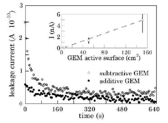
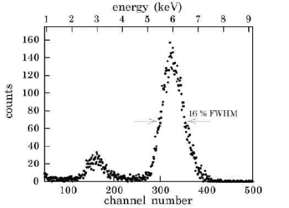
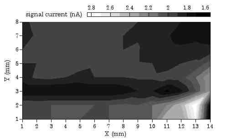
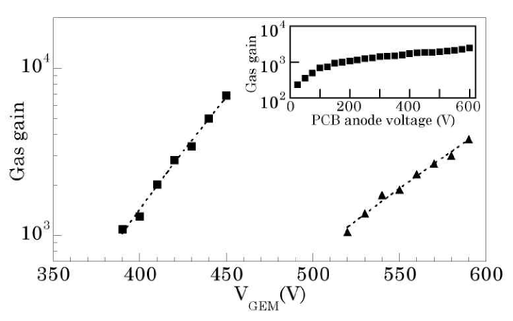
Figs. 7-10 incorporate the extent of our preliminary characterization of subtractive 3M GEMs. Fig. 7 shows typical leakage currents measured in a number of randomly selected GEMs. They consistently display values comparable to previously produced GEMs. However, we have not yet observed any need to “cure” or “burn” 3M GEMs against shorts able to suddenly raise this current into the A range, as is sometimes necessary with other GEMs. The good behavior of these leakage currents over periods of several hours probably comes from the homogeneous surface treatment that the fully-automated roll to roll process guarantees, together with the use of high-purity polyimide, free of any fillers. Each part of each GEM foil receives an identical treatment in every fabrication step, something hard to achieve in manual production runs, especially over large surface areas. For these same reasons we expect a good gain uniformity over large GEM surfaces. An optimal energy resolution in the presence of an uncollimated 55Fe source, as evidenced in Fig. 8, points in this direction. As a matter of fact, first tests of gain uniformity (Fig. 9) yield values already comparable to other MPGDs [20]. Finally, Fig. 10 displays the gas gain measured using the GEMs as an isolated detector, i.e., without a charge collection backpanel anode. We observe no deviation from the expected behavior, nor any anomaly in the onset of discharges (at about VGEM = 450V in Ar + 10% DME and 600V in Ar:CO2).
While the R&D on these GEMs has barely started, all observations are presently very encouraging. First trials with a liquid crystal polymer (LCP) substrate show near-cylindrical hole walls, which can be of interest in applications where excessive dielectric charge-up via ion deposition is a concern (this can lead to a diminished gain uniformity across the surface). Other advantages of LCP compared to KAPTON [21] are a much smaller maximum water absorption (0.02% vs. 2%, which may result in lower outgas, of relevance in HEP applications where extreme gas purity is required), better dielectric properties and a higher chemical and heat resistance. The last may result in GEMs more compatible with soldering and operation in commonly used etching detector gases such as CF4, and possibly more resistant to sparking. We expect to be able to report on LCP-GEMs soon.
Hopefully the methods presented here will enable the production of large area MPGD’s. These will be required in large next-generation time-projection chambers, the leading candidate for the tracking system at the next linear collider [22] and also a possible contender in future underground physics experiments [10]. Proposals for hadron-blind GEM-based detectors in heavy-ion physics programs may similarly benefit [23].
Tested GEM samples can be obtained from collar@uchicago.edu. JIC and PB would like to thank Q. Guo for his assistance in performing SEM and AFM measurements and T. Witten for helpful discussions. JM and IPJS thank Kirk Arndt and Tom Smith of the Department for Physics at Purdue University for technical support.
References
- [1] F. Sauli, Nucl. Instr. Meth. A461, 47 (2001).
- [2] A. Oed, Nucl. Instr. Meth. A471, 109 (2001); L. Shekhtman, Nucl. Instr. Meth. A494, 128 (2002).
- [3] Y. Giomataris, Ph. Rebourgeard, J.P. Robert, and G. Charpak, Nucl. Instr. Meth. A376, 29 (1996).
- [4] http://www.biospace.fr/en/xray.php
- [5] J. Derré, Y. Giomataris, Ph. Rebourgeard, H. Zaccone, J. P. Perroud and G. Charpak, Nucl. Instr. Meth. A449, 314 (2000).
- [6] R. Chechik, M. Balcerzyk, A. Breskin, A. Buzulutskov, G.P. Guedes, D. Mormann and B.K. Singh, Nucl. Instr. Meth. A, in press.
- [7] F.A.F. Fraga , S.T.G. Fetal , L.M.S. Margato, I. Ivaniouchenkov, R.F. Marques and A.J.P.L. Policarpo, 1999 IEEE Nuclear Science Symposium Conf. Rec., Piscataway, NJ, USA. IEEE Part 2, 829 (1999); M. Li, M.S. Dixit and P. Johns, Nucl. Instr. and Meth. A471, 215 (2001).
- [8] E. Costa, P. Soffitta, R. Bellazzini, A. Brez, N. Lumb and G. Spandre, Nature 411, 662 (2001).
- [9] A. Sharma, CERN Courier 41(2001) (http://www.cerncourier.com/).
- [10] J.I. Collar and Y. Giomataris, Nucl. Instr. Meth. A471, 254 (2001) (hep-ex/0009063).
- [11] P. Barbeau, J.I. Collar, J. Miyamoto and I. Shipsey, Procs. of the 2002 IEEE Nuclear Science Symposium and Medical Imaging Conference, Norfolk VA, November 10-16, 2002, submitted to IEEE Tran. Nucl. Sci. (hep-ex/0212034).
- [12] F. Sauli, Nucl. Instr. Meth. A386, 531 (1997); F. Sauli, US Patent #6,011,265, granted January 4, 2000.
- [13] See for example, A. Buzulutskov, A. Breskin, R. Chechik, G. Garty, F. Sauli and L. Shekhtman, Nucl. Instr. Meth. A443, 164 (2000); L. Guirl, S. Kane, J. May, J. Miyamoto and I. Shipsey, Nucl. Instr. Meth. A478, 263 (2002).
- [14] E. Jan Vardaman, Circuit World 26, 15, September 2000.
- [15] T.R. Bergstresser and J.S. Sallo, Procs. of the IPC Chip Scale and BGA National Symposium Proceedings: Pursuit of the Perfect Package, May 6-7, 1999, Santa Clara, CA, USA, vol.1, p. 143.
- [16] B. Chou, S. Beilin, H. Jiang, D. Kudzuma, M. Lee, M. McCormack, T. Massingill, M. Peters, J. Roman, Y. Takahashi and V. Wang, Procs. of the 1999 International Conference on High Density Packaging and MCMs, April 6-9, 1999, Denver, CO, p. 270; J. Geissinger, F. Keller, S. Trevino and T. Kamei, Procs. of the Twenty Seventh Annual IEEE/CPMT/SEMI International Electronics Manufacturing Technology Symposium, 17-18 July 2002, San Jose, CA, USA, p. 41.
- [17] R. Bouclier, M. Capeans, W. Dominik, M. Hoch, J.C. Labbe, G. Million, L. Ropelewski, F. Sauli and A. Sharma, Procs. of IEEE Trans. Nucl. Sci. (USA), 3-9 Nov. 1996, Anaheim, CA, USA, 44, no.3, p. 646.
- [18] J. Benlloch, A. Bressan, C. Buttner, M. Capeans, M. Gruwe, M. Hoch, J.C. Labbe, A. Placci, L. Ropelewski, F. Sauli, A. Sharma and R. Veenhof, IEEE Tran. Nucl. Sci. 45, 234 (1998).
- [19] Low Level Measurements, Keithley publication no. 1559, 5th edition.
- [20] S. Beirle, U. Werthenbach, G. Zech and T. Zeuner, Nucl. Instr. Meth. A423, 297 (1999); S. Kane, J. May, J. Miyamoto, I. Shipsey and I. Giomataris, 2001 IEEE Nuclear Science Symposium Conf. Rec., Piscataway, NJ, USA. IEEE Part 1, 265 (2002).
- [21] T.F. Hayden, Procs. of the 2002 International Conference on Advanced Packaging and Systems (ICAPS), Reno, Nevada, March 10 - 13, 2002; R. Yang, Advanced Packaging, March 2002, (http://ap.pennnet.com/).
- [22] M. Schumacher, Procs. of Physics and Experiments with Future Linear e+e- Colliders. LCWS 2000. Batavia, IL, USA. 24-28 Oct. 2000, AIP Conf. Procs. 578, 821 (2001).
- [23] C. Aidala, B. Azmoun, Z. Fraenkel, T. Hemmick, B. Khachaturov, A. Kozlov, A. Milov, I. Ravinovich, I. Tserruya, S. Stoll, C. Woody and S. Zhou, Nucl. Instr. Meth. A, in press.