The MINOS Light Injection Calibration System
Abstract
A description is given of the light-injection calibration system that has been developed for the MINOS long-baseline neutrino oscillation experiment. The system is based upon pulsed blue LEDs monitored by PIN photodiodes. It is designed to measure non-linearities in the PMT gain curves, as well as monitoring any drifts in PMT gain, at the 1% level.
keywords:
Light injection , calibration , LED , PMT , MINOSPACS:
29.40.Vj , 29.40.Mc1 MINOS overview
The MINOS experiment [1] will investigate the phenomenon of neutrino oscillations [2, 3, 4] by sending a beam of muon neutrinos 735 km through the Earth from the Fermi National Accelerator Laboratory (FNAL), near Chicago, to a detector in the Soudan Underground Mine State Park in northern Minnesota. The experiment uses three detectors:
-
1.
The Near Detector (ND) at FNAL. This will determine the characteristics of the neutrino beam before it begins its journey. Only neutrino events and cosmic ray muons are measured here; there is no “test beam” available.
-
2.
The Far Detector (FD), situated 713 m underground in the Soudan mine, where the neutrino beam emerges from the Earth. Like the near detector, this measures only neutrino events and cosmic ray muons.
-
3.
The Calibration Detector (CD) at CERN is a small detector, similar in structure to both near and far detectors, that is being exposed to particle beams at CERN to study its response to electrons, muons and hadrons of known energies.
2 MINOS detectors
The MINOS far detector is an 8 m wide octagonal tracking calorimeter, consisting of 486 layers of one-inch-thick steel interleaved with scintillator, giving a total mass of 5.4 kilotons. It has a toroidal magnetic field of strength approximately 1.3 T.
Each plane of scintillator consists of 192 strips, each 4 cm wide and 1 cm thick with a co-extruded TiO2 cladding to maximise internal reflection. Light from these strips is wavelength-shifted from blue to green and carried within acrylic fibres [5] to Hamamatsu [6] multi-anode photomultiplier tubes situated around the edge of the detector. Scintillator strips are in orthogonal directions in alternate planes. This gives a 3D readout with an energy resolution of approximately for electromagnetic showers and for hadronic showers. The magnetic field allows measurement of the muon momentum by curvature (14% resolution for a 10 GeV muon) as well as by range for stopping muons (giving approximately 6% resolution).
2.1 Calorimeter energy calibration
In order to measure the neutrino mixing parameters and precisely, the energy response of the detectors has to be calibrated to within a few percent. The goal is a 5% absolute measurement of the energy in each detector, and consistency to within 2% between the near and far detectors. This is carried out in several stages [7]:
-
•
A light-injection calibration system is required to monitor, and to compensate for, changes in amplification (and non-linearity) of the photomultiplier tubes used in the detectors. The light-injection system is the principal subject of this paper.
-
•
Cosmic-ray muons are used to perform the strip-to-strip calibration within each detector, and the relative calibration between the near and far detectors [8, 9]. The strip-to-strip calibrations do not require a high statistical precision ( per strip per month), as both muon tracks and hadronic showers contain many strips. There are expected to be about 530 cosmic ray hits/strip/month in the far detector, giving an accuracy of 2.4% per strip per month, and about 25,000 hits/strip/month in the near detector, giving an accuracy there of 0.3%/strip/month.
Stopping muons can be used to provide the relative calibration of near to far detectors. There are estimated to be 700 stopping muons per day in the far detector, and two orders of magnitude more than this in the near detector. This yields a 1% statistical precision for the near-far detector calibration each day.
-
•
A study to compare the energy deposition by muons with that from hadrons and hadronic showers is being carried out with the calibration detector in a charged-particle test beam at CERN.
2.2 Optical readout

The MINOS readout chain is illustrated schematically in Fig. 1. A 1.2 mm Kuraray Y11 wavelength-shifting fibre [5] lies in a groove along the length of each scintillator strip. Between 16 and 28 such strips are enclosed in a light-tight aluminium case, known as a module. There are eight modules in a full plane.
The wavelength-shifting fibres run to a connector at the end of the aluminium case. Clear fibres [10] then carry the light to boxes containing Hamamatsu multi-anode photomultiplier tubes.
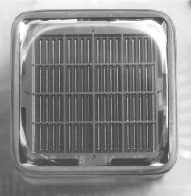
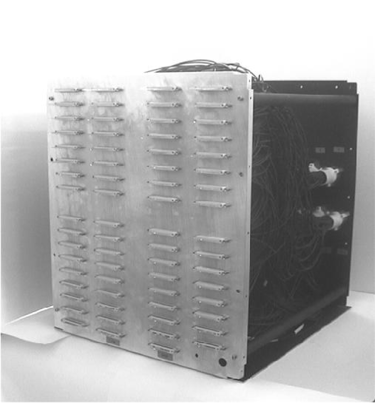
For the far detector, Hamamatsu M16 photomultipliers [11] are used (see Fig. 2), with fibres from eight separate scintillator strips feeding each PMT pixel. This “optical multiplexing”, which provides a substantial saving in the cost of readout electronics, is possible because the event rate at the far detector is so low that there will never be more than one event in the detector at any one time. The typical width of a shower event in MINOS is 50 cm, so the 1 m spacing between strips illuminating a single pixel is appropriate. The multiplexing pattern is slightly different on each side of the detector in order to aid deconvolution.
The far-detector readout electronics uses a modified version of the Viking VA chip [12] made by IDE AS of Norway [13]. This is an integrated circuit containing 32 channels of shaping amplifiers and track-and-hold circuitry. When triggered, each channel is digitised in turn. The data are then transferred to VME readout control crates, with single-board computers running the VxWorks real-time operating system.
Instantaneous event rates in the near detector will be higher than in the far detector. The near detector therefore uses QIE [14] electronics, a high-speed, multi-ranging ADC system with no dead time. Its principal difference from the far detector electronics is that it divides input signals into 19 ns time buckets, and digitises each separately. These separate digitisations are recombined during the event-building process. The light-injection calibration system incorporates an external trigger that can be used to produce optical pulses at different starting positions within the 19 ns time bucket, in order to investigate any possible systematic differences in response at the bucket boundaries.
The near detector is not optically multiplexed (although its muon spectrometer section is electronically multiplexed). It uses Hamamatsu M64 (64-anode) photomultiplier tubes, and has a total of 12,000 readout channels. Unlike the far detector, only one end of each strip is read out: the other end is terminated with a reflector to maximise the detected light. The calibration detector will use both near and far detector readout systems, in order to carry out a systematic comparison of the responses of each.
3 Light-injection system overview
The light-injection system is based upon pulsed blue light-emitting diodes (LEDs). A rack-mounted box, known as a “pulser box”, contains a set of 20 LEDs, each of which has an optical fan-out allowing it to illuminate multiple individual fibres. These fibres carry light to a set of optical connectors on the back panel of the pulser box.
From the pulser box, optical fibres carry the light to the outer edges of the MINOS detector. A set of highly-reflective cavities situated there – the “light-injection modules” – allows the blue LED light to illuminate the green wavelength-shifting fibres, thus producing pulses of light that mimic the signals from the scintillator.
The intensity of injected light is monitored by PIN photodiodes that are read out simultaneously with the PMTs.
In the following sections, the requirements of and constraints upon the light-injection system are discussed, after which each component of the system is examined in detail.
4 Light-injection system requirements
4.1 Aims
The purpose of the light injection system is fourfold:
-
1.
Mapping the gain curve. The response of the photomultiplier tubes becomes non-linear at light levels exceeding about 100 photoelectrons [11]. The light injection system is designed to be able to characterise the response of every optical readout channel on a regular basis (up to once per month in routine operation).
-
2.
Monitoring short-term gain drifts. The gain of a photomultiplier tube is sensitive to small changes in temperature and in applied high voltage. By injecting light at a single point on the gain curve on an hourly basis, any resulting changes in gain can be monitored closely and compensated for.
-
3.
Evaluating PMT gain. Pulsing at very low light levels allows the acquisition of single photoelectron spectra for each channel, from which the gain can easily be calculated.
-
4.
Confirming optical path integrity. The light injection system provides a quick and thorough check to ensure that no fibres are broken.
4.2 Design constraints
A number of constraints were imposed upon the design of the light injection system:
-
1.
The amount of light applied to any pixels on a given PMT that are illuminated simultaneously should differ by no more than a factor of two. This helps to avoid excessive non-linearities and possible problems from crosstalk when injecting light towards the top end of the dynamic range. It is also useful in reducing the amount of data required in order to cover the dynamic range for all pixels, as one does not then have dimly and brightly illuminated pixels that require separate calibration operations at different levels of LED brightness.
-
2.
The M16s used on the far detector are multiplexed, with eight fibres carrying light to each pixel. No two fibres on any pixel may be illuminated simultaneously. Adjacent pixels should also be avoided if possible, to minimise crosstalk problems.
-
3.
The dynamic range of light injected must range from a fraction of a photoelectron up to several hundred photoelectrons on all pixels. Furthermore, this dynamic range should be covered with a step size of the order of one photoelectron.
-
4.
The relative levels of light injected must be measured by a separate device having a response that is linear to 1%, in order to characterise the non-linear response of the PMTs. PIN photodiodes were selected for this purpose.
-
5.
The response of the PIN photodiodes must be stable to within 1% over the timescale of a month.
-
6.
The relative arrival times of the optical pulses at each PMT must be stable to within approximately a nanosecond.
5 Light-emitting diodes
5.1 LEDs vs. lasers
Previous experiments needing light-injection calibration of the type required for MINOS have often used scintillator excited by pulsed lasers, with a variety of neutral-density filters to provide the required dynamic range in light intensity. The development over recent years of the so-called “ultra-bright” blue LEDs enabled a simpler, solid-state system to be considered. Lasers retain three advantages: they are several orders of magnitude brighter than even the brightest LEDs; the pulses are extremely fast, which can better mimic the pulses produced by the passage of charged particles through scintillator; and the spectrum of light produced by the scintillator is almost identical for data and for calibration pulses. For MINOS, however, these possible benefits of lasers were outweighed by the many other advantages of LEDs. LEDs exhibit minimal pulse-to-pulse fluctuations in intensity, so the response of the PMT is dominated entirely by photoelectron statistics. In an LED-based system, there are no moving parts to wear out or break, so the system is appropriately robust for long-term remote operation. In addition, there are no laser parts requiring regular replacement, servicing or gas supplies; the light intensity can be changed by software, instead of relying upon neutral-density filters which may become burned (and therefore non-linear) and which also can only be adjusted slowly; and high repetition rates are possible, so calibration can be carried out quickly. The temporal profile of the optical pulse can be changed to some extent, to explore any effects thereof. Finally, the LED system costs less than a comparable laser-based system. A major factor driving the cost difference is within the fibre plant: blue LED light can propagate down polymer fibre which has a very high absorption at the UV wavelengths generally produced by lasers.
The LEDs used in the pulser system are wide-angle Hewlett-Packard HLMP-CB30 [15]. Initial development work had been done with the LEDs made by Nichia Chemical Industries [16]; the change to the HP LED was forced as Nichia altered the specification of their LED to one having a much slower response, which made the pulses unacceptably long.
5.2 Maximum current
A nominal maximum current specified by the manufacturer of 100 mA is determined by heating effects, which can damage the plastic lens in which the LED is set; however, this is not a problem with the extremely low duty cycle in the MINOS pulser circuit (some tens of nanoseconds per millisecond), and tests showed no sign of damage with currents as high as 500 mA. The MINOS pulser circuit uses a maximum current of 200 mA; above this, the visible light output begins to saturate, and the quality of the pulse shape deteriorates.
5.3 Lifetime
None of the LEDs tested have ever reached the limit of their lifetime. In one instance, the tests included pulses equivalent to 2,000 years of normal MINOS operation, with no adverse effects observed.
5.4 Comparison of spectra
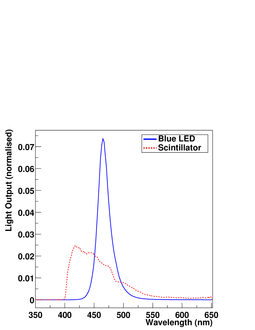
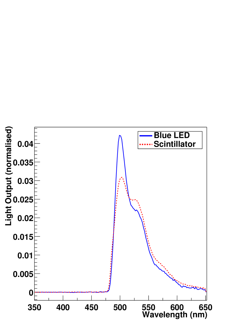
Fig. 3 shows a comparison of the spectra of light emitted from the blue LED with light from an excited piece of MINOS scintillator [17]. The spectra are quite different. When the light is absorbed and re-emitted by the wavelength-shifting fibre, however, the spectra are far better matched, as shown in Fig. 4. The measurement was made using a 300 mm piece of WLS fibre, half of which was glued into a groove in a 150 mm length of MINOS scintillator in the usual manner. The laser light was injected approximately halfway along the scintillator; the LED illuminated the WLS fibre at a point adjacent to the end of the scintillator (and thus approximately halfway along the WLS fibre). Light from the end of the WLS fibre was transported through a quartz fibre to a monochromator and calibrated photomultiplier tube. In MINOS, the situation will be slightly different: most signal pulses will have a much longer path through the green fibre, where self-absorption reduces the short-wavelength component of the light [18], whereas the blue LED light will be absorbed at the very end of the green fibre. Nonetheless, the similarity of the spectra eliminates any concerns about wavelength-dependent ageing of the photocathode (which, in any case, should occur on a timescale much longer than the one-month period over which the light-injection system is required to monitor gain stability).
5.5 Pulse shape
A short, intense pulse of light in a PMT does not necessarily yield the same integrated charge as an identical amount of light delivered over a longer time, and so it is important that the shape of the optical pulse arriving at the photocathode from light injection should be similar to that from the detection of charged particles.
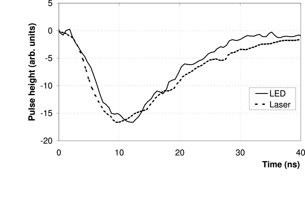
The LEDs have a risetime of 3-10 ns, depending upon pulse height. The fluorescence time of the WLS fibres is typically 7-8 ns, and is specified to be less than 10 ns [19]; the risetime of the signal pulses also increases by 0.7 ns per metre of WLS fibre [18]. Fig. 5 shows the time-averaged shapes of a series of optical pulses from the WLS fibres excited by a blue LED and by scintillator that has itself been stimulated by a nitrogen laser [20]. In each case, the pulses liberated about four photoelectrons from the photocathode: this is approximately the signal size that we would expect from each end of a MINOS far-detector scintillator strip following the passage of a minimum-ionising particle through its centre. The pulse shapes are almost identical in the two cases, and they are dominated by the response of the WLS fibre. In general, the risetime of the LED has little effect upon the overall pulse shape.
5.6 Stability
The short-term pulse-to-pulse variation of an LED was measured by a PIN photodiode circuit with amplifier and a digital oscilloscope. The standard deviation of the pulse height distribution, which is actually dominated by electronics noise from the measurement circuit, was found to be 1.1% of the mean value. Therefore, when the response of the PMT to these optical pulses is measured, the spread in measured light levels is dominated entirely by photoelectron counting statistics; there is no need to account for LED variations on a pulse-by-pulse basis.
However, the LED light output does suffer occasional jumps (typically once every few weeks), and these can sometimes amount to changes of several percent. An independent measurement of light intensity is therefore needed to monitor the output of the LED, and a PIN photodiode was chosen for this purpose.
6 PIN photodiodes
The PIN photodiode used to monitor the relative light output from the LEDs is the Hamamatsu S5971 [6]. This was chosen primarily because it offers a fast response while still having a large enough surface area to accommodate the 1.0 mm diameter light-distribution fibres. Some characteristics are listed in Table 1.
| Active area size | 1.2 mm diameter |
|---|---|
| Spectral response | 320 nm to 1020 nm |
| Dark current | 0.07 nA typ. |
| Temperature coefficient of dark current | |
| Photosensitivity @ 470 nm | 0.24 A/W |
| Temperature coefficient of photosensitivity | at laboratory temperatures |
6.1 Stability
The light injection system is required to be stable as it tracks PMT gain changes over a period of about a month, during which time sufficient numbers of cosmic-ray muons will be detected to calibrate the detector. The stability was tested by pulsing an LED continuously over a period of two months, and monitoring its output several times per second with a pair of PIN photodiodes. After integration and shaping, these were read out by a digital oscilloscope (Fig. 6).

The results of the stability test are shown in Fig. 7. Each point in the figure is an average of a thousand consecutive readings: this is representative of the averaging that will take place during the MINOS calibration. For clarity, only one data point in sixteen is plotted. Over the first ten days, the signal from PIN 1 gradually decreased; this is thought to be caused by the fibre settling slightly in its connector. The sudden jump in LED brightness at day 13 is unexplained, as is its instability in days 25-26; but the intensity changes were recorded by both PIN photodiodes, and the ratio of PIN outputs remained constant. A weekend power cut left the system off for an extended period in days 36-38; when restarted, the LED output returned to its original value. The feature at 46 days occurred when the apparatus was accidently mechanically disturbed—a sharp deviation in one PIN’s signal is again apparent, followed by a slow return to roughly the previous level.
Although the light output of the LED changed by a few percent during the test period (e.g. the step changes at days 13 and 37), the ratio between the individual PIN readings remained constant to within about 0.5% over a period of two months: this is well within the MINOS stability specification.

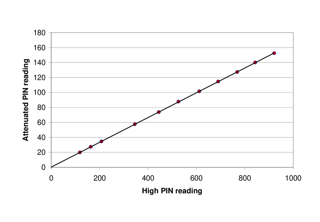
6.2 Linearity
The PIN photodiode must provide a scale that varies linearly with applied light, in order to calibrate the non-linearities of the PMT. The linearity of the PIN photodiode/amplifier system was measured by comparing the signal from a pulsed LED with the signal from the same LED, but with a neutral-density filter blocking most of the light. The amplified and shaped output from the PIN photodiode was read out by a digital oscilloscope in peak-finding mode. Repeating this measurement for several different pulse heights spanning the range of operation of the system produced the linear response shown in Fig. 8. No evidence of non-linearity was observed.
The charge digitisation of the PIN photodiode pulse is also required to be linear. A charge-injection system calibrates the ADC readout channels to an accuracy of 1%, thus ensuring that the PIN photodiode ADC scale is indeed proportional to the light input.
6.3 Readout
In the far detector, two PIN photodiodes are mounted on each of the front-end readout cards. The current pulses produced by the PIN photodiodes are integrated and amplified, producing peak voltages that are a.c. coupled to the VA chips to achieve the required current injection. The VA chip, whose primary purpose is to read out PMT pulses, requires a PMT dynode signal to trigger its readout. The optical wiring ensures that the PMT that triggers the readout of a given PIN photodiode will always be illuminated by the same LED as the PIN photodiode in question. Each LED is in fact served by two PIN photodiodes, mounted on separate front-end readout cards; this allows one readout card to be replaced (to change a PMT or to replace an amplifier) whilst the LED calibration is held by the other PIN photodiode, which remains undisturbed.
In the near detector, the phototubes are read out by QIE electronics, which cannot be used to trigger the PIN readout. Instead, the readout of the PIN photodiodes is triggered by the presence of a signal on the dynode of a separate PMT (discussed in Section 7 below).
The optical fan-out from the LEDs is designed to deliver more light to the PIN photodiode than to the PMT pixels, in order to accommodate the relatively low sensitivity of the PIN. In this way the full dynamic range of the signals is well matched between PIN and PMT. The signal-to-noise ratio of the PIN photodiode circuit is approximately 4000:1 at full scale.
7 Trigger PMT
At times, it will be necessary to take spectra of the PMT response at the single-photoelectron level. In a significant fraction of events no signal will then be seen in the PMT, and consequently the PIN photodiode will not be read out. In order to count these events properly, and in order to provide a distinctive identification to all light-injection events, each pulser box has an additional LED that emits a consistently bright flash with each pulse, regardless of the brightness of the primary LED pulse. Light from this additional LED is carried to a dedicated M16 PMT – the trigger PMT – which is read out in the usual way, thus inserting a unique identifier in the data of each light-injection event. In the near detector the trigger PMT serves an additional function, in that its dynode signal forces the readout of all PIN photodiodes.
8 Mechanical design
8.1 Pulser boxes
Each pulser box is 21 inches high, and fits in a standard 19-inch rack. It is divided by a bulkhead wall into two compartments: one, at the front of the box, is for electronics; the other is for fibre optics. The 20 LEDs are mounted on two circuit boards, supported on trays in the electronics compartment. A controller board, containing the microprocessor and an RS232 interface, connects the two LED driver boards.
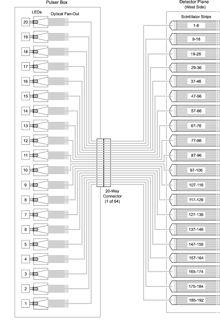
The LEDs overhang the ends of their circuit boards and pass through holes in the bulkhead into optical fan-outs known as cones. Each cone has a set of 71 optical fibres (including spares and dedicated, centrally-located fibres to carry light to PIN photodiodes). These fibres take the optical signals from the cones to four columns of 16 connectors on the back panel (Fig. 9) of the box; each back-panel connector holds 20 fibres – one from each cone. There are three additional 20-wide connectors on the back panel — two provide light to the PIN photodiodes (and so are fed by the dedicated PIN photodiode fibres), and the third is a spare. There is also a single-fibre connector carrying light to the trigger PMT.
Bundles of 20 fibres mounted externally to the box transport the light from each of the back-panel connectors to the 20 light-injection points on each side of each far-detector plane; this is illustrated in Figure 10. The optical routing in the near detector is identical, except that there are fewer light-injection points on each plane (eleven for fully instrumented planes, seven for partially instrumented planes, and on one side of the detector only). The calibration detector has just three light-injection points on each side of each of its 60 planes, and is thus served by six LEDs in a single pulser box.
8.2 Cones and ponytails
The basic design for the optical fan-out is a conical hole bored longitudinally through an aluminium cylinder, with the LED seated at the apex and the 71-fibre bundle attached at the base, as shown in Fig. 11.
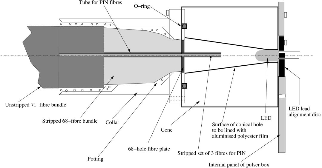
The walls of the cone are lined with aluminised polyester (with a reflectivity greater than 99%) to maximise the intensity of light delivered to the fibres and to assist with the uniformity of illumination of the fibre bundle. The fibre bundle, or “ponytail”, is glued into a plastic collar which is attached to the cone. During assembly, the ends of the fibres are positioned precisely within the collar by means of a plastic disc with holes drilled in it, known as a “tea-strainer”. The surface of this is fly-cut with a diamond-tipped tool.
Three fibres (including one spare) are designated to serve the PIN photodiodes. These are placed in the centre of the fibre bundle. To provide more light, these fibres are extended towards the LED, and are encased in a rigid plastic tube for support (see Fig. 11). This also assists in reducing the non-uniformity of illumination of the light-injection fibres, as the PIN photodiode fibres occupy the area of brightest illumination. Fig. 12 shows the uniformity of illumination of a typical fibre tea-strainer. In this example, the RMS deviation is approximately 15% of the mean value, and the ratio of maximum to minimum intensities is 2.28. On later production models the uniformity improved somewhat, with the ratio of maximum to minimum intensities often lying below 2.0.

The PIN photodiode fibres are significantly longer than all other fibres in the ponytail (6 m vs. 0.8 m). This minimises the differences in relative arrival times of the optical pulses at the PIN photodiodes and at the PMT photocathodes, by compensating for the different optical path lengths: this ensures in turn that the amplified and shaped pulse from the PIN photodiode readout circuit is sampled and digitised at its peak.
A disassembled cone and collar are shown in Fig. 13.
8.3 Optical fibre
The optical fibre used has a 1 mm diameter core of polymethyl methacrylate, with a fluorinated polymer cladding, and was manufactured by Mitsubishi Corp. [21]. The attenuation at 473 nm (the wavelength of the blue LEDs) is approximately 0.08 dB/m. The fibre is jacketed with 2.2 mm diameter opaque black PVC that has a UL-VW1 [22] flame-resistance rating, a fire-safety requirement.
8.4 Optical connectors
The multi-fibre connectors, both at the rear of the pulser box and on the mating ends of the external fibre bundles, are made of plastic. Once the fibres have been glued into place, the connectors are fly-cut with a diamond-tipped tool: this provides extremely good optical transmission, of up to 90% for each connector pair, without damaging the fibres and with a considerable saving in manpower over a hand-polishing process. The design for these connectors was adapted from that for the MINOS optical readout connectors.
Individual fibre ends in the light-injection system are all terminated with an H19 metal connector from OMC [23] (for those carrying light to the PIN photodiodes) or a custom-made, slightly larger variant thereof known as the CLRC01 (for those plugged into the light-injection points on the detector). After gluing and light crimping into the connector, these fibre ends are hand-polished to optimise transmission.
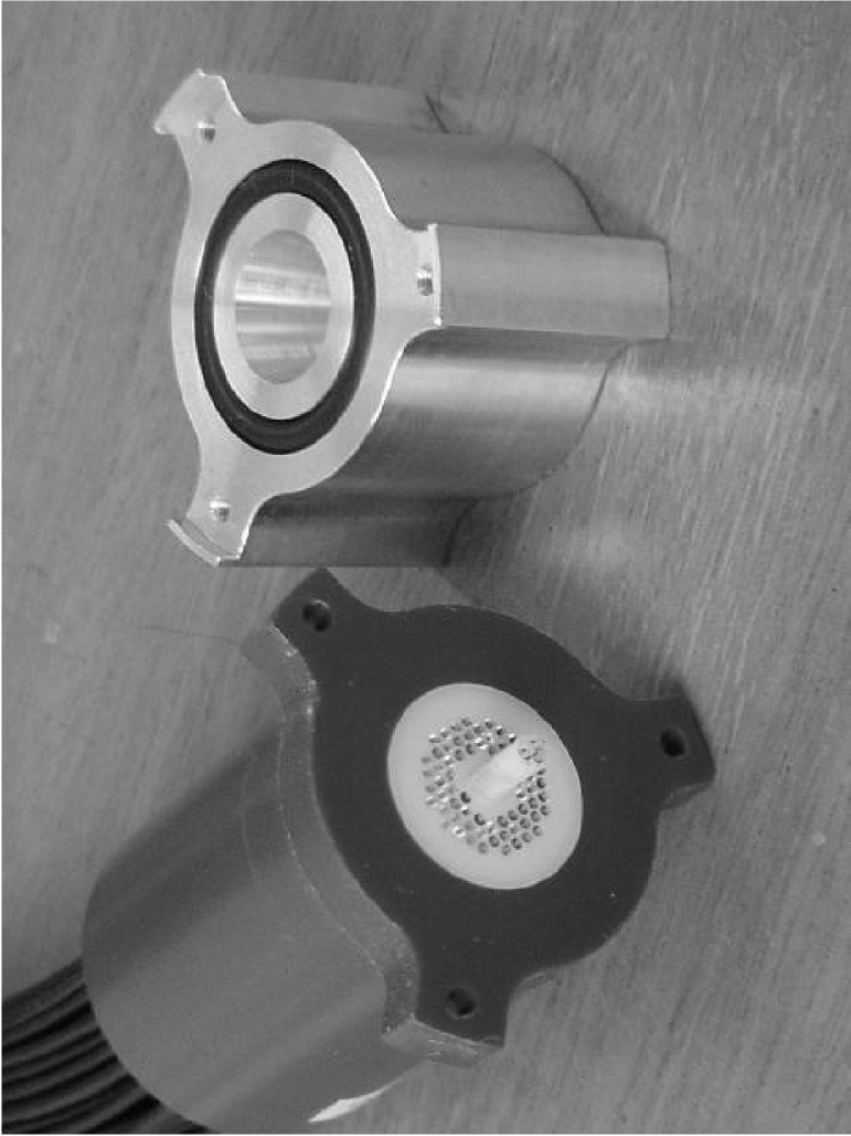
9 Light injection modules


At each end of the scintillator modules, there is a manifold (Fig. 14) that draws the green WLS fibres from the scintillator strips together into a multi-fibre connector. This is the only point of access to the green fibres, and it is here that the LED light enters the optical readout chain. The space is tightly constrained — there is a plane of steel adjacent to the scintillator module on one side, and another just 1 cm away on the other side. This does not allow room for the clear optical fibres carrying LED light to arrive transversely to the planes: instead, they are brought in parallel to the readout fibres. The light illuminates a small (5 cm3) compartment having diffusely-reflecting walls, across the top of which runs a “curtain” of eight or ten WLS fibres. This is illustrated in Fig. 15. The WLS fibres absorb the blue LED light, which is then re-emitted isotropically in the green part of the spectrum. Some of this green light is trapped in the fibre, and propagates in both directions towards the PMTs at either side of the far detector.
The light-injection modules (LIMs; see Fig. 16) containing the compartments (“ashtrays”) in which the absorption takes place are made from injection-moulded black plastic [24], and are mounted on the underside of each detector module, thus forming part of the manifold cover (see Fig. 14). The 16- and 20-wide scintillator modules have two ashtrays in each LIM, and the wider modules have three. A complete MINOS far-detector plane contains 192 scintillator strips, whose green fibres are divided amongst a total of 20 ashtrays. Each ashtray is supplied with the blue light from a single plastic fibre, derived ultimately from one of the 20 LEDs in a pulser box. Each of the LEDs illuminates the same ashtray in up to 64 planes.
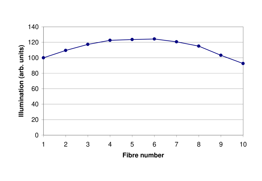
As discussed earlier, the total amount of light illuminating each of the wavelength-shifting fibres should be as uniform as possible. The central position of the light-injection fibre in each ashtray results in a stronger illumination of the fibres at the centre than at the edges of the ashtray. This tendency is countered to some extent by incorporating a curved reflecting back, as shown in Fig. 16, which both shades a portion of the central fibres and reflects more light towards the edges than would a flat back. The uniformity of response across the ashtray is shown in Fig. 17. The walls of each ashtray are coated with a highly reflective -based paint (Bicron BC625).
10 Optical routing constraints
The far detector is eight-fold optically multiplexed. It is essential that only one fibre is illuminated at any one time on any given pixel. As eight or ten adjacent fibres are illuminated simultaneously in an ashtray, this places a constraint on the multiplexing pattern used — any scheme where adjacent strips are mapped to the same pixel is not permissible.

It is also desirable to avoid simultaneous pulsing of adjacent PMT pixels, in order to mitigate the effects of crosstalk [11]. This is the reason for only illuminating up to 10 WLS fibres (one ashtray) at any one time in any given plane. Arranging the fibres from sequential scintillator strips on alternate M16 pixels ensures that the pixels are illuminated in a chessboard pattern, as in Fig. 18, with diagonal rather than edge-adjacent pixels being illuminated simultaneously. The mapping is staggered on one side of the plane so that a hit can be located in the plane by using both ends of the readout.
These considerations lead to a simple algorithm for the optical wiring of the pulser boxes. Each connector at the back of the pulser box contains one fibre from each of the 20 LEDs, and the 20 fibres from each such connector feed the 20 ashtrays of one end of a single plane. Thus, any given LED illuminates up to ten green fibres on each of 64 planes.
11 Electronics
The LED pulser offers the ability to change both the height and the width of the pulse electronically, by varying the current pulse that is applied to the LED. Each pulser box contains up to 20 LEDs, although in the near detector only 11 LEDs are used. As discussed in Section 7, the controller card incorporates an additional “trigger” LED that pulses at a fixed intensity and which is used to flag light-injection events in the data stream.
11.1 Pulser control
The pulser box is controlled by a PIC16F877 microprocessor [25]. It communicates with a control PC via ASCII commands over a serial RS232 link. To avoid a proliferation of different types of data-carrying cable running around the detector, the signals are carried over the detector Ethernet, and converted for the pulser box by an Ethernet-RS232 converter. In the standard mode of operation, the PC instructs the system to pulse a given LED a certain number of times (typically 1000) at a given height, width, and frequency (from 0.5 Hz to 1 kHz). The microprocessor then controls the actual pulsing. The pulser box is also supplied with an external trigger input, which forces a pulse of its current height/width setting in response to a TTL signal. This can be used in the near detector to investigate the effects of the timing of a pulse with respect to the 19 ns time buckets in the QIE electronics.

Fig. 19 shows the LED driver stage from the pulser box circuit. The applied voltage, which determines the pulse height, is controlled by a 10-bit DAC. When the signal at A goes high, the driver stage is turned on — voltage is applied to the 22 resistor, and the current is shunted to ground via the left-hand FET. This occurs typically a microsecond before the actual pulse, to give the current time to stabilise. (This “bypass” current is turned off between each pulse in order to avoid excessive heating.) When the signal at B goes low, current flows through the LED, which emits light. A short time later, signal C goes high, and the current is shunted to ground via the right-hand FET; the LED is then turned off. The pulse width is determined by the delay between B turning off and C turning on; this is controlled by a programmable delay line, giving a current pulse width of 15 to 36 ns in 3 ns steps. The light pulses delivered to the phototube produce signals ranging from a fraction of a photoelectron up to about 500 photoelectrons.
12 Performance
During the summer of 2001, the MINOS calibration detector was placed in a charged-particle test beam at CERN. One of its functions was to confirm that the light-injection system could compensate for changing PMT gains at the 1% level. The calibration detector was fully equipped with MINOS readout electronics.
The gain curves of the PMTs were produced by injecting light at ten different levels, and plotting the response of the PMTs as a function of the PIN photodiode output. Figure 20 shows two such plots, labelled “Old Gain Curve” and “New Gain Curve”, measuring the same channel at different times. Each point represents the mean of 2000 optical pulses. The gain in general was observed to drift only slowly (less than 2% over two months); but at one point the voltage supplied to the PMTs was increased, resulting in the dramatic difference between the two gain curves shown here.
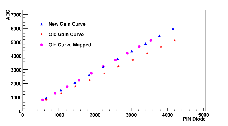
Drift in gain is monitored by looking at specific points on the gain curve on a regular (typically hourly) basis, as discussed in Section 4.1 above. These points are used to calculate a multiplicative factor for each channel that is applied to the entire gain curve so as to mimic the time-evolution of the gain. The underlying assumption is that the actual shape of the gain curve does not change on a short timescale. Figure 20 includes the recalculated gain-curve points.
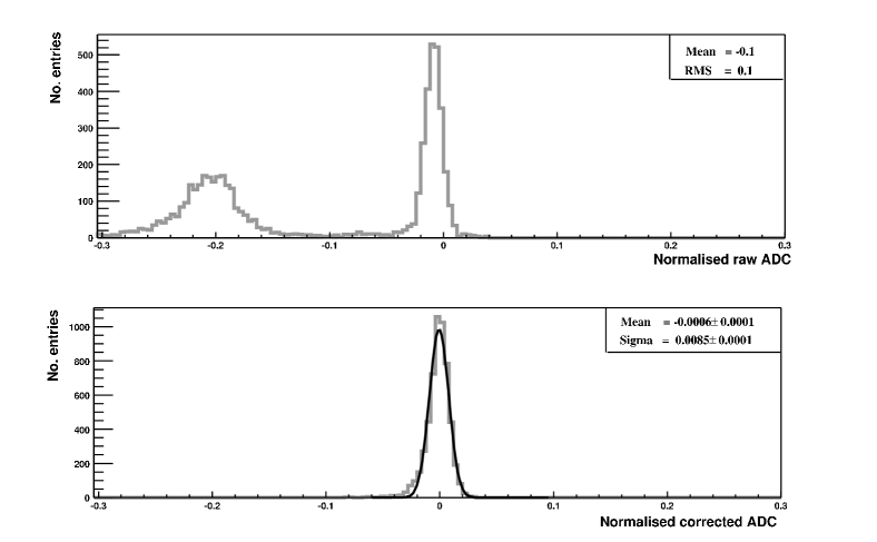
The performance of the light-injection system can therefore be tested by selecting different points on the gain curves, and comparing the mean ADC for a given light input with that predicted from the drift-point calculation. The results of this procedure are shown in Figure 21. The upper histogram shows the relative difference between the means of measured points on separate gain curves, i.e. (ADC(0)-ADC())/ADC(0), and the lower histogram shows the relative difference between the measured and corrected points, i.e. (ADC(0)corr-ADC())/ADC(0)corr. This technique is independent of any changes in light output from the LEDs; any change in gain of the PIN photodiodes would appear as an offset from zero of the lower histogram. The width of the lower histogram is limited by photoelectron counting statistics at each data point: the ultimate precision achievable by the system is not yet completely determined, but the figure demonstrates that the calibration procedure has corrected the gain changes to within the 1% specification required by MINOS.
13 Conclusion
A light-injection system has been developed to assist in the calibration of the MINOS detectors. Based upon blue LEDs, with PIN photodiodes to monitor relative intensities, the system is able to measure non-linearities in PMT response as well as measuring changes in gain at the 1% level on an hourly basis over timescales of a month or more.
Acknowledgements
This work has been funded by the UK Particle Physics and Astronomy Research Council and the US Department of Energy. The authors would like to thank the other members of the MINOS collaboration for their support, and in particular Jim Musser and Karol Lang, both of whom have provided valuable criticism of the document, and the members of the scintillator, DAQ, electronics, and integration/installation groups for all of the time and effort spent in accommodating the needs of the light injection system. Jim Grozier gave generously of his own free time to carry out crucial laboratory tests at Sussex. The assistance of CERN and its PS staff with the test-beam experiments is gratefully acknowledged. The staff at OMC have also been most helpful. This work is based in part on the dissertation of P. Adamson, submitted to the University of Sussex in partial fulfilment of the requirements for the D.Phil. degree [26].
References
- [1] The MINOS Collaboration, MINOS Technical Design Report; FNAL internal document NuMI-L-337 (1998).
- [2] B. Pontecorvo, JETP 34 (1958) 247.
- [3] B. Pontecorvo, JETP 53 (1967) 1717.
- [4] S. Bilenky, S. Petcov, Rev. Mod. Phys. 59 (1987) 671.
- [5] Kuraray Y11(175), MJ, non-S type 1.2 mm diameter with K-27 fluor, from Kuraray Ltd., Tokyo, Japan.
- [6] Hamamatsu Corp., 325-6, Sunayama-cho, Hamamatsu City, Shizuoka Pref., 430-8587, Japan; www.hamamatsu.com.
- [7] G. Feldman, report of the MINOS Calibration Working Group; unpublished.
- [8] P. Litchfield, Presentation to minos calibration working group.
- [9] R. Lee, S. Seun, FNAL internal document NuMI-L-694 .
- [10] Kuraray 1.2 mm diameter clear fibre, from Kuraray Ltd., Tokyo, Japan.
- [11] S. E. K. Lang, J. Day, et al., Nucl. Instr. Meth. A 461 (2001) 571–573.
- [12] O. Toker, S. Masciocchi, E. Nygård, A. Rudge, P. Weilhammer, Nucl. Instr. Meth. A 340 (1994) 572–579.
- [13] IDE AS, Veritasveien 9, Box 315, N-1323 H vik, Norway; www.ideas.no.
- [14] T. Zimmerman, M. Sarraj, IEEE Trans. on Nuclear Science 43 (1996) 1683–1688.
- [15] Hewlett-Packard 3000 Hanover Street Palo Alto, CA 94304-1185, U.S.A.; www.hp.com.
- [16] Nichia Corporation, 491 Oka, Kaminaka-Cho, Anan, Tokushima 774-8601, Japan; www.nichia.co.jp.
- [17] J. Thomas, et al., Nucl. Instr. Meth. A 423 (1999) 320–327.
- [18] P. Border, et al., Nucl. Instr. Meth. A 463 (2001) 194–204.
- [19] B. Choudhary, L. Mualem, FNAL internal document NuMI-L-589 .
- [20] R. Schwienhorst, private communication; data provisionally available at http://www.hep.umn.edu/minos/fiber/timing.html.
- [21] Mitsubishi Rayon Corp., 520 Madison Avenue, New York, NY 10022, U.S.A.; www.mitsubishi.com.
- [22] Underwriters Laboratories; www.ul.com. The VW1 test is described in standard UL 1581, section 1080.
- [23] Optoelectronic Manufacturing Corporation, Redruth, Cornwall, U.K.; www.optomanfcorp.com.
- [24] Polyphenylene Oxide - Styrene (NorylTM grade N190X); www.geplastics.com.
- [25] Microchip Technology Inc., Chandler, Arizona, U.S.A.; www.microchip.com.
- [26] P. Adamson, An LED Calibration System for the MINOS Long-Baseline Neutrino Oscillation Experiment, D.Phil. Thesis, University of Sussex (2001).