Testing of Hamamatsu R5900-00-M64 Multi-Pixel PMTs for MINOS
Abstract
The MINOS long baseline neutrino oscillation experiment is comprised of three calorimeters, a Near Detector at FNAL, a Far Detector at the Soudan mine in northern Minnesota, and a Calibration Detector in a test beam at CERN. The light produced in the interactions of neutrinos in the Near Detector at FNAL will be routed by optical fibres onto the pixels of Hamamatsu R5900-00-M64 multi-anode photomultiplier tubes. This article reports the measurements performed on 15 of these tubes to evaluate them for their use in MINOS.
keywords:
PMT , MINOS , Multi-Pixel PMT , R5900-00-M64NuMI-PUB-SCINT-820
ONUP-2002-??
, , , , , , , , ,
1 Introduction
The MINOS (Main Injector Neutrino Oscillation Search) Experiment has been designed to identify neutrino oscillations[1] and measure their parameters in the controlled environment of the NuMI neutrino beam at Fermi National Accelerator Laboratory (FNAL). The beam of predominantly muon neutrinos will pass through the Near Detector (ND) a calorimeter composed of planes of plastic scintillator and steel, at FNAL where the original flavour composition of the beam will be measured. The Far Detector (FD), a 5.4KT calorimeter of similar composition, situated in the Soudan mine in Northern Minnesota, will measure the flavour composition of the same beam km further away.
Both detectors will use extruded scintillator strips, read out via wavelength shifting (WLS) fibres glued into a central groove, to detect energy depositions of particles traversing the detector. The light from the WLS fibres is transmitted by clear acrylic fibres to 16-pixel Hamamatsu R5900-00-M16[3] photomultiplier tubes (PMTs) in the FD and to 64-pixel Hamamatsu R5900-00-M64 (M64) PMTs in the ND. Two different types of PMTs are required in order to take economical advantage of optical summing, possible in the low rate environment of the FD but not in the high-rate environment of the ND.
The results from testing fifteen M64s are reported in this paper.
The article is organised as follows: Section 2 describes the requirements on the tubes from the MINOS experiment while Section 3 gives technical details about the M64. Results from dark noise measurements are given in Section 4, while Section5 describes the details of the measurements of different PMT properties.
2 Required performance of PMTs for MINOS
The main requirements on the PMT characteristics are the following:
-
-
good single photoelectron (p.e.) sensitivity;
-
-
linearity up to 200 p.e.;
-
-
single-channel gain above and up to ;
-
-
small inter-pixel cross-talk;
-
-
uniformity of response that does not significantly change in the presence of a magnetic field of up to gauss;
-
-
tube dark count rate of less than kHz above a p.e. threshold.
In order to achieve the proposed physics goals, MINOS has to detect minimum ionising particles (MIPs) and has to measure electromagnetic showers. For a MIP, the energy released in the scintillator corresponds to about p.e. per strip traversed. On the other hand, electromagnetic showers can produce light signals as large as 200 p.e. It is therefore of the utmost importance that the photodetectors used have a wide dynamic range: they must be able to measure single p.e. signals precisely while still behaving as linear devices at light levels of up to 200 p.e.
The digitisation of the PMT signals is carried out roughly 1 m away from the tubes. Therefore, to avoid any effect due to electromagnetic pick-up noise, the PMT gain should be greater than .
Due to the high beam intensity at the near detector, up to neutrino events may be present within the same s spill shortly after the primary protons hit the neutrino production target. To minimise complications in the event reconstruction algorithms, cross-talk to all neighbouring pixels of the same PMT should be below 10%.
The PMTs will be located close to the magnetised steel planes, where a fringe field of about gauss is expected. The PMT will be installed inside a steel housing, which will act as a shield and should reduce the field by at least . However, it is important to verify that the tube response is not significantly affected by the remaining field and to have a safety margin.
All hits are continuously digitised by the front-end electronics and sent via readout processors to a “trigger farm”, which decides, depending on the event pattern, whether or not to save the data for further analysis. As the processing power and the bandwidth of the transfer are limited, it is important that the performance of MINOS is not affected by the presence of noise. The dark count rate of a single PMT channel should therefore be limited to about Hz. This is mainly due to bandwidth limitations of the DAQ system. The digitisation of all anode channels is started by the presence of a sizeable signal on the common last dynode. It is therefore important to study the noise properties of the anodes as well as of the last dynode.
3 Technical characteristics of M64 PMTs
Before describing in detail the procedure to evaluate the performance of the PMTs, it is useful to summarise the technical characteristics of the average M64 PMT as provided by Hamamatsu Photonics[4].
The Hamamatsu R5900-00-M64 is a -dynode multi-anode PMT, with a transverse section of inches. The pixels (2 mm 2 mm) are arranged on an square grid. These pixels are separated from each other by a distance of less than 0.3 mm, but there is a region of reduced collection efficiency extending to 0.3 mm.
Focusing electrodes run over the pixels which guide the photoelectrons into the dynode structure. Each pixel has two identical dynode chains associated with it which terminate in a single anode pad.
The cathode and the housing of the tube are at negative potential and a tapered bleeder circuit is used to apply voltage to the dynodes. The divider ratio adopted for the present measurements is the one recommended by Hamamatsu for optimal performance (). Decoupling capacitors at the last stages help to keep the potential differences constant between the last dynodes and the anode in the presence of large instantaneous currents. The main parameters for the average PMT, as provided by Hamamatsu, are summarised in Table 1.
The only data available concerning the quantum efficiency (QE) of the PMTs are those given in the Hamamatsu data sheets. Fig. 1 shows QE as a function of the incident light wavelength for tubes. The mean value of QE at nm, the wavelength of interest for MINOS, is 13.5% with a spread of 0.9%.
For ten of the tubes, Hamamatsu measured the anode dark count rates at V and after minutes in the dark. The distribution of measured rates is shown in Fig. 2. Integrating over all the channels, the dark count rate is approximmately Hz. This is well below the maximum rate acceptable for MINOS.
| Parameter | Description/Value |
|---|---|
| Photocathode material | bi-alkali |
| Spectral response | 300 to 650 nm |
| Quantum efficiency (QE) at 520 nm | 12.0 % |
| Wavelength of maximum QE | 420 nm |
| Window material | borosilicate glass |
| Window thickness | 0.8 mm |
| Material of metal casing | KOVAR |
| Weight | g |
| Dynode type | metal channel structure |
| Number of stages | 12 |
| Anode | array of 8 8 independent pixels |
| Anode dark current per channel | 0.2 nA |
| Pixel size | 2 mm 2 mm square |
| Maximum high voltage | 1000 V |
| Gain at 800 V (typical) | (1)3105 |
| Anode pulse rise time | 1.5 ns |
| Transit time spread per channel (FWHM) | 0.3 ns |
| Pulse linearity per channel ( 5 %) | (1) 0.6 mA |
| Uniformity between each anode | 1:3 |


4 Dark Noise
The light signal released by a minimum ionising particle in MINOS can be as low as two photoelectrons. It is therefore extremely important to study the PMT dark noise at very low threshold levels. Since the last dynode signal will be used in MINOS to trigger the anode readout, the dark count rate has to be measured for dynode thresholds corresponding to anode signals of approxiately photoelectron.
4.1 Set-up description
A block scheme of the experimental set-up used for these measurements [7] is shown in Fig. 3. The PMT under test is connected to its base and placed into a dark box. A removable plug is used to allow light into the otherwise light-tight box. The high voltage is supplied to the PMT by a Hewlett-Packard DC power supply (HP-E3631A) through a DC/DC converter circuit and monitored by a digital multi-meter (HP-34401A). Both are connected to a PC ( MHz, Pentium III processor) through a GPIB interface.

The signals from the last dynode and from the anode pixel under study are sent via a coaxial cable and an amplification stage (Phillips 779, nominal gain ) to a four-channel Tektronix digital oscilloscope (TDS 540A). All the remaining anode channels are terminated through to prevent charge build-up. The oscilloscope bandwidth is limited to 100 MHz to reduce noise.
The PC communicates with the oscilloscope via a LabVIEW based program. Once the triggering conditions have been set and the channel whose data will be acquired has been selected, the program reads in the waveform of the PMT pulse event by event and measures:
-
-
the baseline level, to account for any DC offset by the amplifier;
-
-
the signal amplitude.
The oscilloscope acquires 910 pulses at a rate in excess of 10 kHz before transferring the data to the PC. The oscilloscope is inhibited during the transfer which takes about one second.
To obtain an absolute measurement of the gain, although not crucial for the determination of the dark count rate, a voltage-to-charge conversion factor of has been measured by assuming shape universality for the PMT pulses.
4.2 Anode dark noise
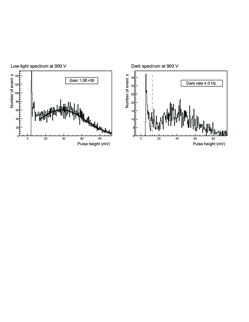
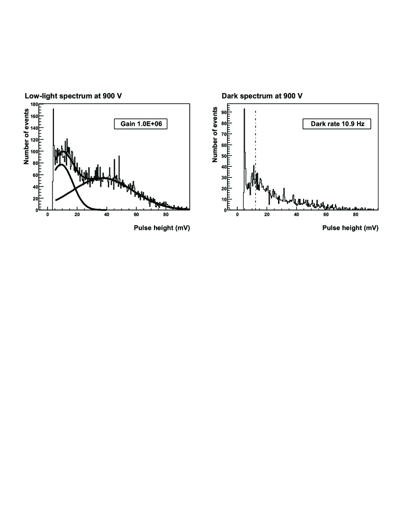
Each of the tubes under test was kept in the dark and under high voltage ( V) for at least six hours before performing the actual measurement. Low-light spectra and dark spectra were taken at high voltages between and V for all pixels in one quadrant of the tube. The oscilloscope trigger threshold was set just above the anode pedestal peak which is at zero, as evidenced in Fig. 4 which shows the falling edge of the pedestal at very low pulse heights. The dark count rate was determined using an offline threshold of 1/3 of a photoelectron.
For all of the measured tubes, the low-light spectra of the pixels belonging to the inner matrix show a distinct single-photoelectron peak, well separated from the electronic noise. These pixels typically have relatively low dark count rates (a few Hz). Typical low-light and dark spectra of such pixels are shown in Fig. 4. Pixels along the edges of the PMT generally have higher noise rates, although in most cases still within acceptable limits. Of greater concern is the shape of their low-light spectra, since quite frequently the single-photoelectron peak is not very well distinguishable from the dynode noise contribution. Moreover a second peak, distinct from the noise but at pulse heights below the single-photoelectron peak, is often present (see Fig. 4). This is due to photons passing through the photocathode and hitting the first dynode where they are absorbed and a single photoelectron is emitted. This results in a peak in the distribution corresponding to an amplification of one dynode stage less than the main one photoeletron peak. The different behaviour between the inner and the outer pixels is expected to be due to different focusing conditions as well as to the difficulty in keeping the fabrication process uniform across the entire photocathode area.
The dependence of the dark noise on the PMT high voltage has also been studied. This is shown in Fig. 5. The dark count rate increases at higher values of high voltage. The single anode dark count rate at V is measured to be Hz, with a spread of Hz.

The temperature dependence of the dark count rate has been measured for one PMT. For both inner and outer pixels the gain does not vary substantially with temperature, while, as expected for bi-alkali photocathodes, the dark count rate increases exponentially with temperature (( per ∘C; see Fig. 6).

4.3 Dynode dark noise
The last dynode is common to all anodes, and so its single-photoelectron spectrum can be viewed as the sum of charge distributions, each of them corresponding to the single-photoelectron signal on one of the pixels. As the gain is different for each channel, in general no clear peak is visible when the spectrum is acquired by triggering on the dynode signal itself.
It is necessary to determine the noise rate at the dynode caused by signals above p.e. from the lowest gain pixel. To do this, the PMT was illuminated at a very low level. Initially, the spectrum from the lowest gain pixel was digitized and confirmed to be mostly one p.e. signals. Then, the pulses from this pixel were used to trigger the oscilloscope while the dynode signal was digitized. This enabled us to measure the contribution to the dynode spectrum from this channel and to determine the dynode threshold level which corresponded to p.e. on the lowest gain pixel as shown in Figure 7.
After light-sealing the dark box again, the PMT was kept under high voltage and in the dark for more than 24 hours. A dark spectrum of the last dynode was taken, triggering on the dynode signal itself. In order to reach the necessary sensitivity to the dark count rate, the trigger threshold had to be tuned somewhat below the p.e. level ascertained in the previous measurement, but high enough not to be dominated by electronic noise. Knowing the acquisition time, the integral dynode dark count rate as a function of the trigger threshold can be computed from the pulse height distribution. Knowing the relative positions of the anode and of the last dynode 1 p.e. peaks, the gain of the last amplification stage can be computed from simple charge conservation considerations. At V, the gain of the last dynode is .
The integral dynode dark count rate as a function of the trigger threshold, which was obtained for both settings of high voltage, is shown in Fig. 7 for one of the PMTs. The count rate for a threshold of p.e. is equal to about at and to about at ; as expected, the higher the gain, the higher the dark noise.
Following the procedure described above, the last dynode dark count rate at p.e. has been measured for all the available PMTs at V and after hrs in the dark. The resulting distribution for the 15 tubes is shown in Fig. 8. The mean value is about Hz, which confirms that the tubes under test are extremely quiet.


5 Results from PMT scanning
Most of the properties of the PMTs have been studied by measuring the phototube response to a point-like light source, which has been moved across the photocathode surface. This procedure is referred to as a “PMT scan”.
5.1 Set-up
Two different set-ups have been independently developed, and most phototubes have been tested in both setups. While in one set-up the PMT was moved to scan the light source across the photocathode, the other assembly used a moving plastic fibre. The results achieved with both setups are consistent. We therefore only describe the latter apparatus in detail. A schematic view of the setup with the movable fibre is shown in Fig. 9 [7].
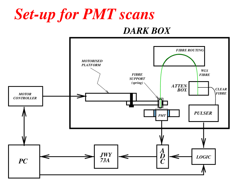
The PMT under test is mounted into the scanning apparatus with the help of a tightly fitted plastic collar, which in turn is mounted onto an aluminium PMT holder. In order to prevent bad connections between the PMT and the base sockets, the base is screwed to the PMT holder from the back.
Light output from a programmably pulsed blue LED at a repetition rate of 16 kHz is used to illuminate the PMT. The blue light is carried by a clear acrylic fibre to an attenuation box. In this box the clear fibre is mounted at a fixed distance (90 degree angle) to a 1 m long WLS fibre[6] in a similar LED illumination scheme as used in the MINOS scintillator modules. The WLS fibre carries the light to the PMT surface. For the measurements described here, the level was set to be between a few and 200 photoelectrons. To prevent possible transmission changes in the WLS fibre while moving it across the PMT cathode, a routing device was used to constrain the fibre to slide in an arc-shaped groove ( cm diameter, 0.5 cm width). The fibre was connected to a non-magnetic armature that is in turn screwed to a motorised platform. This arrangement moves the fibre across the photocathode. The fibre itself is fitted into a black plastic cylinder which is gently pressed against the glass window by a spring.
The high voltage is supplied to the PMT as in the dark noise set up. The motorised platform is powered by a SmartDrive SA46 base unit, containing two D28 drives. The drives are controlled by a Trio Motion Technology Euro205 Motion Coordinator linked to the PC via a serial interface.
The 64 PMT anodes are connected to LeCroy 2249A ADC modules ( bits, pC/count sensitivity); these are read out by a Jorway 73A CAMAC crate-controller coupled to the PC via a SCSI connection. Trigger signals from the LED pulser, coinciding with the light pulses, are used to gate the ADCs. The whole set-up is controlled by a LabVIEW 5.1 program and events are taken at a rate of kHz, i.e., not every light pulse is digitised.
The standard program of measurements for a PMT consists of the following steps:
-
1.
an alignment run, to get the PMT centre coordinates with respect to the scanning table home position;
-
2.
point scans (WLS fibre at the centre of the pixels) at different high voltages ( 850, 900, 950 V) and light levels (from a few to 100 photoelectrons);
-
3.
determination of the lowest gain pixel and measurement of the dynode dark count rate at p.e. (see Section 4).
At the beginning of each scan a pedestal run is acquired, to determine the zero offset for each ADC channel. For each fibre position events were recorded, and the ADC information for all of the channels was stored as one-dimensional histograms.
5.2 Tools and Techniques
5.2.1 Alignment
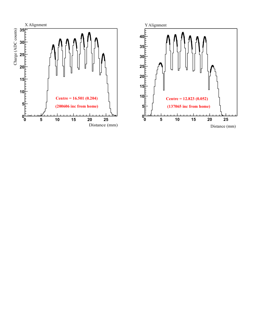
Every time a tube was installed in the PMT holder, an alignment run was performed before running the actual scan in order to determine the position of the PMT centre with respect to the home position of the scanning table. The home position is known to within m.
The alignment run consists of two scans, one along a row of the PMT -axis and the other along a column -axis, with a step size of m points per scan and with statistics of events per point. For each point, the pulse height in the pixel with the largest signal is plotted against the position of the WLS fibre: the profiles obtained in this way are similar to those in Fig. 10. The structure of the profile closely reflects the geometry of the PMT pixel: the peak amplitudes are proportional to the corresponding pixel gain. Each peak is fitted with a Gaussian function. The central position is calculated as the average of the eight fitted centres.
Several tests have been conducted in order to assess the reliability of the apparatus, especially concerning the reproducibility of its geometry and of the alignment procedure[7]. Our studies show that the position of the PMT centre on the transverse plane is known to within m along the axis and to within along the axis. Moreover, no appreciable effect from any rotation around the PMT symmetry axes has been observed.
5.2.2 Photon Statistics
In order to make measurements of gain and efficiency, it is necessary to have an estimate of the amount of light impinging on the photocathode. It is possible to make such an estimate by assuming that the number of photoelectrons emitted at the photocathode is described by Poisson statistics and that the amplification processes initiated by different photoelectrons along the dynode multiplicative system are independent. In this case the mean value () and the RMS () of the pedestal-subtracted charge distribution of the PMT are given by:
| (1) |
where is the PMT gain. The number of photoelectrons and the PMT gain are then
| (2) |
This method, referred to as the ‘photon-statistics method’, is the one used in the following paragraphs to calculate gain and number of photoelectrons for any analysed PMT. The method is known to be inaccurate in several respects:
-
•
It does not take into account the fluctuations in the number of electrons produced at the first dynodes, i.e. the width of the one-photoelectron peak). Due to the sensitivity of our electronics we could not measure these fluctuations and did not correct for them.
-
•
If the tube response is non-linear, becomes a function of and Eqs. (2) are no longer strictly valid. However, the measurements of efficiency and gain were all done at a level of approximately 10 p.e. where the tubes are in their linear regime.
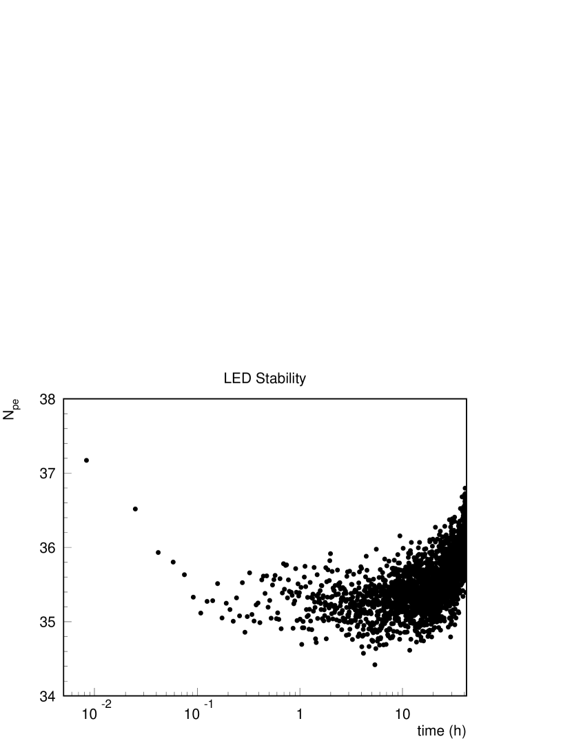
It is still meaningful to use Eqs. (2) in order to separate gain and number of photoelectrons to compare different PMTs. We have verified that the LED pulser is a stable light source (Fig. 11); therefore the number of photoelectrons gives us a measure of the relative efficiency of the pixels within a tube. The efficiency here is a product of the collection efficiency (CE) and the quantum efficiency (QE). An absolute measure of the efficiency is not possible as the light source was not calibrated. The absolute value of the gain is estimated to be accurate to within approximately .
5.3 Results
5.3.1 Gain dependence on high-voltage
Scans at approximately 10 p.e. have been used in order to minimise possible effects arising from non-linearities, but still having sufficient sensitivity. The gains for all pixels of the tested PMTs have been measured at different high voltages (HV).
The plots in Fig. 12 show the average gain of all pixels for all of the 15 tubes as a function of HV ( V). The gains of the pixels with the highest and lowest gains in each tube are also shown. The average gain increases from about at V to about at V. Although MINOS running will require gains of , corresponding to high voltages of lower than 850V, the sensitivity of the electronics used in this test was not sufficient to evaluate the PMTs at that voltage.
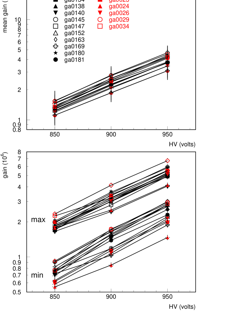
The nominal gain spread (, the gain ratio of the minimum and maximum gain pixels) for M64 PMTs is 1:3 (). The average ratio measured is about at V and reaches at V with small differences between different tubes. The fact that decreases with decreasing HV is probably an artifact of saturation effects, which become more important at higher gain. Similar features can be recognised in Fig. 13, which shows the ratio between each channel gain and the maximum gain of the same PMT, where runs over the PMT index and runs over the pixel number. The 15 entries at in each histogram correspond to the 15 maximum gain pixels.

5.3.2 Cross-talk
As all channels were read out constantly during the PMT scans, it was straightforward to measure the PMT cross-talk. The cross-talk for a fibre position has been defined to be
| (3) |
where is the charge of channel and the sum runs over a certain class of neighbouring channels. All charges are averaged over 10,000 events. The cross-talk into direct or diagonal channels as well as the total cross-talk has been measured. Most of the cross-talk is into direct neighbours and only much reduced cross-talk into diagonal pixels was observed. Results are summarised in Fig. 14, where the cross-talk for all the tested phototubes is displayed. The total cross-talk is about on average, with long tails extending to . The cross-talk into non-neighbouring pixels sums up to about .

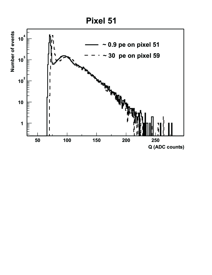
As an example we have plotted the charge distributions for pixel 51 in Fig. 15. This measurement was performed with a modified base (voltage divider ratio ) and using a high bandwidth amplifier to achieve the required sensitivity. Two spectra are compared: The solid spectrum shows the distribution when the pixel itself is pulsed with an average of 0.9 photoelectrons. The dashed distribution had been recorded when the neighbouring pixel 59 was illuminated with approximately 30 photoelectrons. From plots like this one can determine the kind of cross-talk present:
-
1.
A distinct single photoelectron peak is visible when illuminating a neighbouring pixel. This suggests that some of the photons coming through the WLS fibre are not producing a photoelectron at the fibre location, but on adjacent pixels. This can be explained by the divergence of the light leaving the fibre and internal reflections in the PMT glass window.
-
2.
The pedestal peak visible in Fig. 15 is different from the one observed when pulsing the pixel directly. It is shifted to higher values. This shift is proportional to the light level. It is an indication that a constant fraction of charge is seen at the neighbouring anode due, presumably, to charge leaking across to the neighbouring dynode structure during multiplication.
5.3.3 Linearity studies
Photomultiplier tubes are in general reasonably linear devices: the charge at the anodes is proportional to the amount of light incident on the cathode. Nevertheless, when the incident light is too intense or when the bias voltage is too high, significant deviations from the ideal linear response are observed. This is mainly related to the dynode chain linearity characteristics, which are independent of the incident light wavelength and which, at fixed high-voltage values, are functions only of the peak current passing through the last dynode stages[8, 9]. Space charge effects are very important for PMTs operated in pulsed mode when intense light pulses can reach the photocathode and induce large current flows through the last dynode stages in addition to leaving charge between these dynodes. The magnitude of the consequent saturation effect is related to the internal tube geometry, the design of the resistive bleeder circuit, as well as to the electric field intensity and its spatial distribution.
The use of a tapered bleeder circuit (see Sec. 3) reduces such effects, as the large potential differences in the last few stages of the amplification chain enhance the voltage gradient where the electron space density becomes higher. Nonetheless, the M64 phototubes still exhibit a considerable non-linear response, especially when compared to M16 PMTs which is a consequence of the M64’s comparitively smaller pixel size. The different behaviour of the two types of phototubes is very clear in Fig. 16, where the relative outputs of the two photodetectors are shown as a function of the instantaneous PMT current when one pixel is illuminated (Hamamatsu data): while M16s are essentially linear for currents up to about mA, M64s depart from linearity already at about mA.

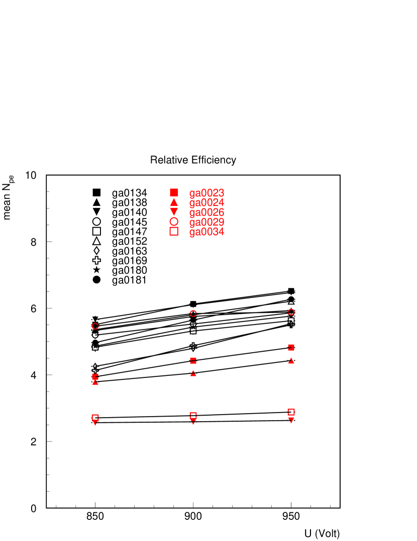
The photon-statistics method, described in Sec. 5.2.2, relies on the assumption that the PMT is a linear device. Assuming that the light source is stable, any deviation from linearity should have a direct effect on the quantities calculated in Eq. (2). This is what is observed in Fig. 17, where , the number of photoelectrons, is plotted as a function of HV. The spread in at fixed HV reflects a general change in light level, when testing different sets of tested tubes. (We had to demount and remount the fibres in the attenuation box leading to a change in overall light level.) It appears that the calculated number of photoelectrons is a function of the applied voltage; but of course the light level cannot really depend on the voltage. To verify that this dependence is an artifact of the photon-statistics computation and not an effect correlated with the PMT quantum efficiency and collection efficiency, in Fig. 18 is plotted as a function of QE at nm and of the calculated gain separately: seems to be independent of QE, while a clear dependence on is observed. Simulations have confirmed that tube non-linearities can influence the calculations of in the observed way when the light level is 30-50 photoelectrons as shown in Fig. 19
At light levels as low as 3-5 photoelectrons the PMT gain fluctuations (width of the single-photoelectron peak) become dominant and influence the calculation. This width varies with gain. The relative width of the single-photoelectron peak becomes narrower as the gain increases, leading to a higher calculated number of photoelectrons.


5.3.4 Sensitivity to Magnetic Fields
To test the potential consequences of a stray magnetic field on the PMT performances, a Helmholtz coil was used to generate a homogeneous field of up to gauss[7]. A full scan (a total of points, points per pixel) of several tubes was performed for each value of the magnetic field. No effect was observed for a field orientation perpendicular to the PMT longitudinal axis (), either on the tube gain or on collection efficiency. However, if the field is parallel to the -axis, significant effects on the collection efficiency of the outer pixels are observed at intensities of gauss and above. Cross-talk was observed not to be affected by the presence of a magnetic field, regardless of its orientation.
6 Conclusions
We have measured the properties of the Hamamatsu R5900-00-M64 multi-anode photomultiplier tube and find that these tubes are well suited for the MINOS experiment. We have found that the main properties of the tube are:
-
-
The quantum efficiency at 520 nm is
-
-
The average tube gain is 1.3 at 850 V while the ratio of minimum to maximum pixel gain is better than 1:3.
-
-
There are only small variations in the tube efficiency. The typical variation has been measured to be .
-
-
There are already sizable non-linearities at a tube gain of .
-
-
When placing a 1.2 mm acrylic fibre on the photocathode, the cross-talk to neighbouring pixels is on average which includes contributions from both optical and charge cross-talk
-
-
Typical dark count rates at are less than 10 Hz per pixel for signals above 1/3 of a photoelectron.
-
-
The tubes are to a large extent insensitive to magnetic fields of up to 5 gauss.
References
-
[1]
K.S. Hirata et al., Phys.Lett. B280 (1992) 146;
Y. Fukuda et al., Phys.Lett. B335 (1994) 237;
D. Caspar et al., Phys.Rev.Lett. 66 (1999) 2561;
W.W.M. Allison et al., Phys.Lett. B391 (1997) 491;
S. Ahlen et al., Phys.Lett. B357 (1995) 481;
Y. Fukada et al., Phys.Lett. B433 (1998) 9;
Y. Fukada et al., Phys.Lett. B436 (1998) 33. - [2] MINOS Collab., The MINOS Detectors, Technical Design Report, NuMI-L-337, 1998.
- [3] K. Lang et al., Evaluation of Hamamatsu R5900-00-M16 Multi-Pixel PMTs for MINOS, to be published in N.I.M. A.
- [4] Hamamatsu Photonics K.K., 325-6, Sunayama-cho, Hamamatsu City, Shizuoka Pref., 430-0193, Japan.
- [5] TPMH1192E03, Hamamatsu Preliminary Data: Multianode Photomultiplier Tube R5900-00-M64, TPMH1192E03, Jan 1999.
- [6] Kuraray Y-11(175) MC, Non-S, J-type fibre, from Kuraray Co. of Japan.
- [7] A.Weber, Private communication. For further information contact a.weber1@physics.ox.ac.uk or http://webnt.physics.ox.ac/minos.
- [8] Philips Photonics, Photomultiplier Tubes: Principles and Applications, Brive Philips, 1994.
- [9] Photomultiplier Tube: Principle to Application, Hamamatsu Photonics K.K., Japan, 1994.