Hybrid Pixel Detector Development
for the Linear Collider
Vertex Tracker
Abstract
In order to fully exploit the physics potential of the future high energy linear collider, a Vertex Tracker able to provide particle track extrapolation with very high resolution is needed. Hybrid Si pixel sensors are an attractive technology due to their fast read-out capabilities and radiation hardness. A novel pixel detector layout with interleaved cells has been developed to improve the single point resolution. Results of the characterisation of the first processed prototypes by electrostatic measurements and charge collection studies are discussed.
keywords:
pixel detectors, vertex detector; linear collideremail: Marco.Battaglia@cern.ch and Massimo.Caccia@mi.infn.it
1 Introduction
The physics programme at future high energy linear colliders, designed to deliver collisions at centre-of mass energies = 0.3 - 3 TeV with luminosities in excess to cm-2 s-1, largely relies on the ability to identify the flavour of final state fermions with high efficiency and purity challenges . This task must be accomplished in a challenging environment due to the large track density from highly collimated hadronic jets and the accelerator induced backgrounds. The estimated track density, 1 hit mm-2, requires the adoption of pixel detector technology. The target performance for the resolution on the track impact parameter, defined as the distance of closest approach to the collision point, has been obtained from detailed studies of jet tagging performances in a variety of physics reactions. These results indicate that a resolution of 5 m 15 m / (GeV/c), or better, has to be achieved. Several conceptual designs have been proposed so far, relying on three alternative sensor technologies: Charge Coupled Devices (CCD) ccd , Hybrid Pixels vertex99 and Monolithic CMOS sensors cmos . This paper summarises recent results on the development of hybrid pixel sensors for the future linear collider applications.
2 Hybrid Pixel Sensor Design
Hybrid pixel sensors, pioneered in fixed target and LEP experiments and further developed for their application in the LHC Vertex Detectors, have several features of interest for application in the linear collider Vertex Tracker. Fast time-stamping capabilities and sparse data scan read-out allow to minimise the effect of beam backgrounds, while their radiation hardness ensures a significant safety margin compared to the anticipated neutron fluence in the linear collider interaction region. At present, their main limitation comes from the achievable single point resolution. A resolution m, required to match the needed impact parameter accuracy, can be obtained by sampling the diffusion of the carriers generated along the particle path and adopting an analog read-out to interpolate the signals of neighbouring cells. Since the charge diffusion r.m.s. in 300 m thick silicon is 8 m, its efficient sampling requires a pixel pitch below 50 m. As the most advanced read-out electronics have a cell dimension of 50 300 m2, this represents the present limit to the pixel pitch. Future developments in deep sub-micron VLSI vlsi may help overcoming this limit. However it is interesting to independently explore sensor designs improving the pixel sensor performances in terms of single point resolution.
The proposed pixel detector design exploits a layout, already successfully adopted in Silicon microstrip detectors, where only one-out-of- implants is read-out. In such a configuration, charge carriers generated underneath one of the interleaved pixel cells induce a signal on the capacitively coupled read-out pixels. The ratio of the signal amplitudes at the left- and right-hand side of the read-out pixels is proportional to the distance of the position of crossing of the particle from the read-out node. In this design the sampling of the charge carrier distribution is achieved by the implant pitch and the analog cell size has to fit the wider read-out pitch. The ratio between the inter-pixel, , and the pixel-to-backplane, , capacitances defines the signal amplitude reduction by charge loss to the backplane. This signal reduction and the two track separation performances limit the number of interleaved pixels.
3 Hybrid Pixel Sensor Tests
Prototypes of detectors with interleaved pixels have been designed and manufactured sitges . Thirty-six test structures have been fit on a 4 wafer, consisting of detectors with 0 to 3 interleaved pixels defining a VLSI cell size of either 200 200 m2 or 300 300 m2. The structures have been characterised by electrostatic tests. About half of the tested structures exhibit a leakage current of 10 nA/cm2, or less, at full depletion and a breakdown point well beyond the full depletion voltage. The inter-pixel and backplane capacitances, crucial to determine the feasibility of the proposed sensor layout, have been directly measured on different structures and the results compared to a numerical estimate obtained by solving the Laplace equation inside a 55 pixel matrix with a finite element analysis package opera . The results have been found to be in fairly good agreement. The computed values for the single pixel capacitance are summarised in Table 1.
| Det 1 | Det 2 | Det 3 | Det 4 | |
|---|---|---|---|---|
| Implant width (m) | 100 | 60 | 50 | 34 |
| Implant pitch (m) | 150 | 100 | 75 | 50 |
| total () | 22.31.1 | 12.70.6 | 11.80.6 | 8.60.4 |
| to nearest () | 3.70.2 | 1.90.1 | 1.80.1 | 1.30.1 |
| () | 7.31.1 | 3.20.7 | 1.90.7 | 0.80.2 |
From these values, the charge loss to backplane has been estimated to be 50% for the geometries adopted in the present test structures, thus allowing an effective signal interpolation.
The charge collection properties of the test sensors have been directly studied by shining an infrared diode spot on the backplane of a structure with 60 m implant width, 100 m implant pitch and 200 m read-out pitch. At the diode wavelength of = 880 nm, the penetration depth in the silicon substrate corresponds to 10 m. The IR light has been focused to a spot size of 80 m and its position parallel to the detector plane controlled by a 2-D stage allowing to scan the pixel array with micro-metric accuracy parallel and orthogonal to the pixel rows. A matrix of 4 7 read-out pixels has been wire-bonded to a VA-1 chip. For each spot position, 1000 events have been recorded. The common mode, pedestal and noise calculation has been initialised for the first 300 events. In the subsequent events light was injected every 10 events, allowing for continuous pedestal tracking. Because of the limited data volume, no on-line suppression has been applied and the data reduction and cluster search has been performed off-line. Results have been averaged over the 70 recorded light pulses. Figure 1 shows the recorded pulse height as a function of the scan position. The charge loss has been measured by comparing the cluster pulse height for the laser spot positioned on either an interleaved or a readout pixel. The results are shown in Figure 1, where pulse heights are normalised to their maximum value. The observed charge loss does not exceed 50 %, in agreement with the expectations from the capacitance measurements.
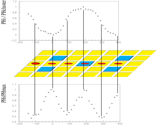
The charge sharing can be characterised by the shape of the distribution defined as , where is the pulse height recorded on the ith read-out pixel in the cluster and the total cluster pulse height. The measured curve, shown in Figure 1, exhibits the expected correlation between the distance of the point of charge creation from the leftmost strip and the response, where corresponds to the particle hitting the ith pixel and to the particle traversing the sensitive volume half-way between the ith and the (i+1)th read-out pixel. The observed functional dependence can be interpreted as the superposition of the effects of the charge diffusion and the capacitive charge sharing.
4 Conclusions
Prototype pixel detectors with interleaved pixel cells, aimed at improving their single point resolution to match the requirements for applications at the future linear collider, have been designed and manufactured. The results of their electrostatic characterisation and the preliminary charge collection studies have confirmed the validity of this detector concept.
References
- (1) M. Battaglia, in these proceedings.
- (2) A. Gillman, in these proceedings.
- (3) M. Battaglia et al., Nucl. Instr. and Meth. A 447 (2000), 202.
- (4) M. Winter, in these proceedings.
- (5) M. Campbell, in these proceedings.
- (6) M. Caccia et al., In Proc. of the Worldwide Study on Physics and Experiments with Future Linear Colliders, E. Fernandez and A. Pacheco (editors), UAB, Barcelona 2000, vol. II, 893.
- (7) OPERA-3D, software package by Vector Fields Ltd., 24 Bankside, Kidlington, Oxon, OX5 IJE, UK.