Beam Test Results of the BTeV Silicon Pixel Detector
Abstract
The results of the BTeV silicon pixel detector beam test carried out at Fermilab in 1999-2000 are reported. The pixel detector spatial resolution has been studied as a function of track inclination, sensor bias, and readout threshold.
, , , , , , , , , , , , , , , , , , , , , , and
1 Introduction
The BTeV collaboration has intensively beam-tested several single chip silicon pixel detector prototypes and front-end readout chips, in order to establish the basic parameters of the pixel sensors and readout chips which will be used as the building blocks of the BTeV vertex detector[1]. To study the pixel detector spatial resolution, a reference silicon telescope was used to project the incident beam track to the pixel sensor under test. Of particular interest was a comparison of the resolution obtained, using 8 bit and 2 bit charge information, for a variety of incident beam angles (from 0 to 30 degrees). Moreover, the spatial resolution was studied as a function of sensor bias and readout threshold.
2 Experimental setup
The tests were performed in the MTest beamline at Fermilab, with a 227 GeV/c pion beam incident on a 6 plane silicon microstrip telescope (see Figure 1), with several single-chip silicon pixel planes placed in the middle of the apparatus.
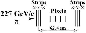
The pixel sensors tested have 50 m 400 m pixel size and are all from the “first ATLAS prototype submission [2]”; up to four pixel detectors could be tested simultaneously. The silicon microstrip detectors (SSD) were read out using SVX-IIb ASIC’s[3] and the data acquisition system was based on VME, adapted from the CDF SVX test stand[4]. The extrapolation accuracy of the silicon microstrip telescope at the pixel detectors location was 2.1 m for tracks with shared charge in adjacent SSD channels. The excellent spatial resolution was due to the small strip pitch (20 m) and the high pion momentum available (which minimized the multiple scattering).
The readout was triggered by the coincidence of signals from two 15 cm 15 cm scintillation counters, positioned upstream and downstream of the silicon telescope and separated from each other by about 10 m. In order to select tracks incident on the active area of the pixel detectors, the FAST_OR output signal from one of the FPIX0-instrumented pixel detectors was also required.
2.1 FPIX0 and FPIX1 readout chips
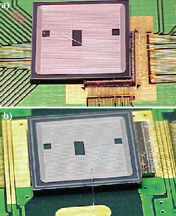
The FPIX0 readout chips were indium bump bonded by Boeing North America Inc. to CiS sensors (one p-stop “ST1” and one p-spray “ST2”). The instrumented portion of the sensor is 11 columns 64 rows (Figure 2a).
Each FPIX0 readout pixel contains an amplifier, a comparator, and a peak sensing circuit[5]. The analog output is digitized by an external 8-bit flash ADC.
The FPIX1 readout chips were indium bump bonded by Advanced Interconnect Technology Ltd to Seiko sensors (two p-stop ST1’s and one p-spray ST2). FPIX1 is the first implementation of a high speed readout architecture designed for BTeV. It has 18 columns of 160 rows, and is the same size as the ATLAS single chip sensors (Figure 2b). However, a minor design error limited the number of rows which may be read out to 90 per column. Each FPIX1 cell contains an amplifier, very similar to the FPIX0 amplifier, and four comparators, which form an internal 2-bit flash ADC[5].
The pixel detectors were calibrated using a pulser and two x-ray sources (Tb and Ag foils excited by an 241Am -emitter). For most of the data taking, the discriminator threshold for the FPIX0 p-stop was set to a voltage equivalent to 2500400 e-. For the FPIX0 p-spray device the corresponding threshold was typically 2200350 e-. The amplifier noise was measured to be 10515 e- for the FPIX0 p-stop sensor. The corresponding noise values for the FPIX0 p-spray sensor was 80 10 e-. In addition, we found an equivalent charge noise due to the external buffer amplifier and ADC of 400150 e- for FPIX0 p-stop. The corresponding external noise values for the FPIX0 p-spray sensor were 18520 e-. The FPIX1 chips have four threshold inputs (one for each comparator in the 2-bit FADC implemented in every cell). We found a set of four average threshold values in nominal running conditions, for the FPIX1 p-stop, of about and , with a spread of about . The amplifier noise was measured to be . The relatively high FPIX1 readout threshold in the test beam was due to noise and pickup problems in a printed circuit board interface. An FPIX1 test module, with up to 5 chips bump bonded to an ATLAS tile-1 sensor, has been operated stably in bench tests with discriminator threshold set below 1500 e-.
3 Results
3.1 Charge collection
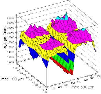
Charge collection can be studied in detail for the FPIX0-instrumented sensors, thanks to the 8-bit analog information and the absolute calibration. Figure 3 shows that the p-spray sensor suffers sizeable charge collection inefficiency between columns, especially on the column boundaries which include the “punch-through biasing” network111These charge losses are thought not to be intrinsic to the p-spray technology, but a feature of this particular sensor design, where each biased n+ implant pixel is surrounded by a floating n+ implant ring. The charge collection inefficiency is believed to be mostly due to the presence of this ring[6]. . Our measurement of this charge loss is consistent with previous measurements made by the ATLAS pixel collaboration[6].
The measured pulse height distributions were fit using a Landau function convoluted with a Gaussian [7]. Figure 4 shows the pulse height distributions for the FPIX0-instrumented p-stop sensor.
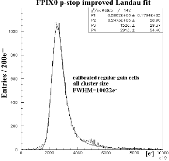
The “improved Landau” function fits the experimental data quite well, except the bump at 50000 e- which is due to saturation of the off-chip buffer amplifier/ADC combination. In addition, about 0.7% of the events have a charge collected in the FPIX0 p-stop sensor less than 15000 e- (for these values the Landau distribution predicts a very small probability), indicating that the p-stop sensor also suffers a very small charge collection inefficiency. Studies show that this inefficiency is concentrated at the four corners of the sensor pixels.
We find that the charge collected by the CiS p-spray sensor is about 24% less than the charge collected by the p-stop sensor. The most probable and average charge collected are respectively 2000070 e- and 2310070 e- for the CiS p-spray sensor (considering only tracks far away from the inter-pixel boundary). For the CiS p-stop sensor, the most probable charge collected is 2473030 e-, and the average charge collected is 3010030 e-.
3.2 Spatial Resolution
The tracks used to study pixel spatial resolutions were fit using data from the SSD telescope and from pixel detectors other than the device under test, using a Kalman-filter. The coordinate measured by a pixel detector is obtained by the position of the center of the cluster of hit pixels associated with a track, plus a correction (conventionally called the function) which is a function of the charge sharing, the cluster width, and the track angle. For this analysis, we have used a linear “head-tail” algorithm for computing the function, which ignores the charge deposited in pixels in the interior of a cluster, and uses only the charge deposited on the edges of the cluster[8]. Two specific examples of residual distributions are shown in Figure 5 with the Gaussian fits superimposed.
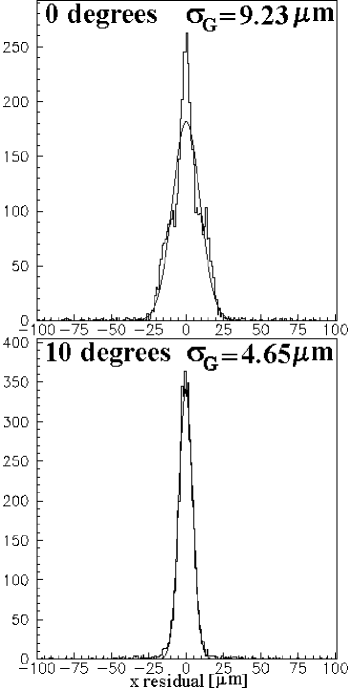
Clearly, the residual distributions are not Gaussian, especially at zero degrees where for a significant fraction of the time only one pixel is hit. The residual distributions also have more entries far from zero than the Gaussian fits. This can be clearly seen in the data taken at ten degrees, when there is always charge sharing. The origin of these “tails” is attributed to the emission of -rays which skew the charge sharing and degrade the resolution. Nonetheless, the Gaussian standard deviations provide a reasonably good characterization of the width of the central peak for both plots.
The residual distribution widths, obtained for several track angles and different detectors, are shown in Figure 6. The experimental results are in good agreement with the simulation results described in [9].
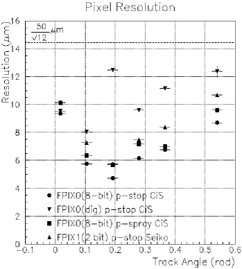
We have also computed residual distributions for this data set without using any charge sharing information. These “digital” resolution results are included in Figure 6. The resolution for the FPIX1-instrumented p-stop detector is slightly worse than the results that we obtained by degrading by software the FPIX0-instrumented p-stop pulse height information to 2-bit equivalents. This is because the main effect degrading the resolution is the high threshold and the 2-bit analog information has only a minor effect. In fact, the FPIX1-instrumented detector was operated with a discriminator threshold of 3780 e-, while the FPIX0-instrumented detector was operated with a discriminator threshold of 2500 e-. Moreover, the results obtained for a p-spray detector with a threshold of 2200 e- show the extent to which the charge losses in the p-spray sensor degrade the spatial resolution.
Figure 7 shows how the position resolution is affected by changes in the sensor bias voltage and the discriminator threshold.
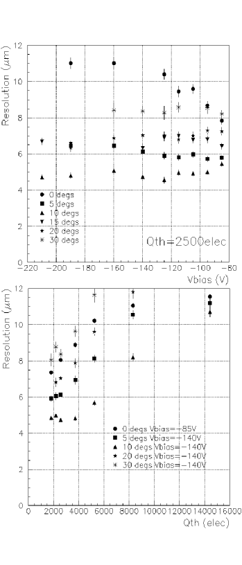
The relative sensitivity of the pixel sensor position resolution to these parameters is very important. In fact, the variation of the bias and effective threshold are similar to what is expected when the radiation damage influences the sensor bulk properties and the charge collection efficiency. The data show, for large track angles, not too much sensitivity to the bias voltage, because the charge-sharing is dominated by the track inclination. At small track angle, when the diffusion gives a substantial contribution to the charge-sharing, the sensor bias is important. The effect of the readout threshold is always significant, but the spatial resolution is still better than up to a threshold of .
3.3 Resolution function shape
The pixel residual distribution (or resolution function) deviates from a Gaussian in two important ways. First, when tracks pass through one pixel only the residual distributions are well fitted by a square function convoluted with a Gaussian. Second, when tracks pass through more pixels we have found that our experimental residual distributions can be fitted by the sum of a Gaussian term and a term which is a square with edges that decrease like a power of 1/x:
| (1) |
where is a normalization constant, is the half width of the constant term, and is the exponent of the power law. Figure 8 shows the experimental resolution functions in log scale taken with the beam nominally at normal incidence for cluster size one and cluster size bigger than one.
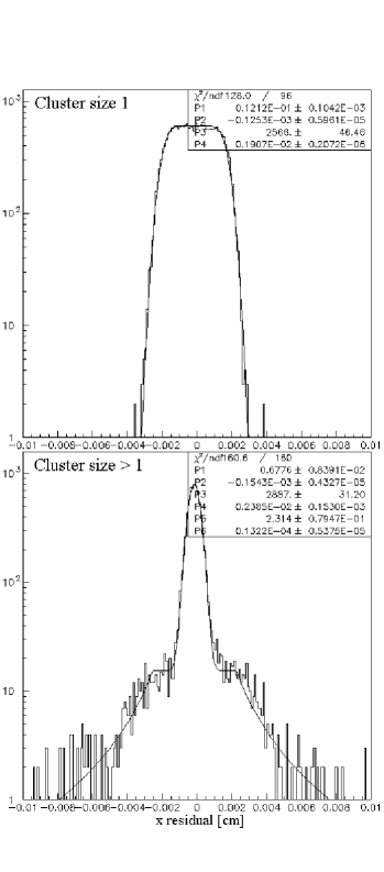
In this last case, we find a satisfactory representation of the data using eq. 1 with the following set of parameters: , m, and set so that accounts for about 18% of the total number of entries in the distribution.
4 Summary
We have described the results of the BTeV silicon pixel detector beam test. The pixel detectors under test used samples of the first two generations of Fermilab pixel readout chips, FPIX0 and FPIX1, (indium bump-bonded to ATLAS sensor prototypes). The spatial resolution achieved using analog charge information is excellent for a large range of track inclination. The resolution is still very good using only 2-bit charge information. A relatively small dependence of the resolution on bias voltage is observed. The resolution is observed to depend dramatically on the discriminator threshold, and it deteriorates rapidly for threshold above .
References
- [1] C. Newsom, Overview of the BTeV Pixel Detector, see these proceedings.
- [2] T. Rohe, et al., Nucl. Instr. and Meth. A409 (1998) 224.
- [3] T. Zimmerman, et al., IEEE Trans. Nucl. Sci. Vol.40 No.4 (1993) 736.
- [4] S. Zimmerman, et al., IEEE Trans. Nucl. Sci. Vol.43 No.3 (1996) 1170.
- [5] D.C. Christian, et al., Nucl. Instr. and Meth. A 435 (1999) 144.
- [6] F. Ragusa, Nucl. Instr. and Meth. A 447 (2000) 184.
- [7] S. Hancock, et al., Nucl. Instr. and Meth. B1:16 (1984) 16.
- [8] R. Turchetta, Nucl. Instr. and Meth. A 335 (1993) 44.
- [9] M. Artuso, Spatial resolution predicted for the BTeV pixel sensor, see these proceedings.